Conductive Paste For Solar Cell Electrode And Solar Cell Manufactured Using Same
KO; Min Soo ; et al.
U.S. patent application number 16/346074 was filed with the patent office on 2020-01-23 for conductive paste for solar cell electrode and solar cell manufactured using same. The applicant listed for this patent is LS-NIKKO COPPER INC.. Invention is credited to Mun Seok JANG, Tae Hyun JUN, Chung Ho KIM, In Chul KIM, Min Soo KO, Hwa Young NOH.
| Application Number | 20200024180 16/346074 |
| Document ID | / |
| Family ID | 62025209 |
| Filed Date | 2020-01-23 |
| United States Patent Application | 20200024180 |
| Kind Code | A1 |
| KO; Min Soo ; et al. | January 23, 2020 |
CONDUCTIVE PASTE FOR SOLAR CELL ELECTRODE AND SOLAR CELL MANUFACTURED USING SAME
Abstract
The present invention relates to a conductive paste for a solar cell electrode, including a metal powder, a glass frit and an organic vehicle, wherein the metal powder includes a metal powder having a sintering shrinkage rate of 15 to 30%, whereby the light-receiving area of the front electrode of a solar cell formed using the conductive paste including the metal powder having an increased sintering shrinkage rate can be enlarged and short-circuit current (Isc) can be increased, thus increasing the power generation efficiency of the solar cell.
| Inventors: | KO; Min Soo; (Seoul, KR) ; KIM; In Chul; (Yongin, KR) ; KIM; Chung Ho; (Namyangju, KR) ; NOH; Hwa Young; (Hwaseong, KR) ; JANG; Mun Seok; (Seoul, KR) ; JUN; Tae Hyun; (Seongnam, KR) | ||||||||||
| Applicant: |
|
||||||||||
|---|---|---|---|---|---|---|---|---|---|---|---|
| Family ID: | 62025209 | ||||||||||
| Appl. No.: | 16/346074 | ||||||||||
| Filed: | October 18, 2017 | ||||||||||
| PCT Filed: | October 18, 2017 | ||||||||||
| PCT NO: | PCT/KR2017/011511 | ||||||||||
| 371 Date: | June 27, 2019 |
| Current U.S. Class: | 1/1 |
| Current CPC Class: | H01L 31/022425 20130101; C03C 4/14 20130101; H01B 1/22 20130101; C03C 8/16 20130101; C03C 2204/00 20130101; C03C 8/18 20130101; Y02P 70/521 20151101 |
| International Class: | C03C 8/18 20060101 C03C008/18; H01L 31/0224 20060101 H01L031/0224; C03C 4/14 20060101 C03C004/14 |
Foreign Application Data
| Date | Code | Application Number |
|---|---|---|
| Oct 31, 2016 | KR | 10-2016-0143687 |
Claims
1. A conductive paste for a solar cell electrode, comprising a metal powder, a glass frit, and an organic vehicle, wherein the metal powder includes a metal powder having a shrinkage rate of 15 to 30%, measured as an area reduction rate after applying, drying and firing the paste including the metal powder, compared to before firing.
2. The conductive paste of claim 1, wherein the metal powder includes a first metal powder having a sintering shrinkage rate of 15 to 20%.
3. The conductive paste of claim 1, wherein the metal powder includes a second metal powder having a sintering shrinkage rate of 20 to 25%.
4. The conductive paste of claim 1, wherein the metal powder includes a third metal powder having a sintering shrinkage rate of 25 to 30%.
5. The conductive paste of claim 1, wherein the metal powder includes at least two metal powders selected from the group consisting of a first metal powder having a sintering shrinkage rate of 15 to 20%, a second metal powder having a sintering shrinkage rate of 20 to 25%, and a third metal powder having a sintering shrinkage rate of 25 to 30%.
6. The conductive paste of claim 5, wherein the metal powder is configured such that an amount of the metal powder having a relatively high shrinkage rate is greater than an amount of the metal powder having a relatively low shrinkage rate.
7. The conductive paste of claim 1, wherein the metal powder has an average particle diameter (D50) of 0.5 to 5 .mu.m.
8. A solar cell, comprising a front electrode provided on a substrate and a rear electrode provided under the substrate, wherein the front electrode is manufactured by applying, drying and firing the conductive paste of claim 1.
Description
TECHNICAL FIELD
[0001] The present invention relates to a conductive paste for use in the formation of an electrode of a solar cell and a solar cell manufactured using the same.
BACKGROUND ART
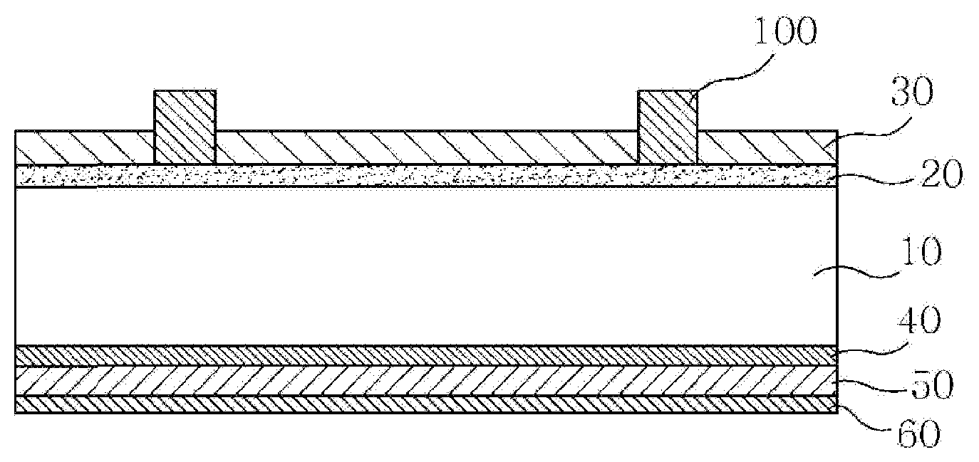
[0002] Solar cells are semiconductor devices that convert solar energy into electrical energy, and typically have a p-n junction type, and the basic structure thereof is the same as a diode. FIG. 1 shows the configuration of a general solar cell device. The solar cell device is typically configured using a p-type silicon semiconductor substrate 10 having a thickness of 180 to 250 .mu.m. An n-type impurity layer 20, having a thickness of 0.3 to 0.6 .mu.m, is formed on the light-receiving surface of the silicon semiconductor substrate, and an antireflective film 30 and a front electrode 100 are formed thereon. A rear electrode 50 is also formed on the rear surface of the p-type silicon semiconductor substrate.
[0003] The front electrode 100 is formed by applying a conductive paste containing conductive particles of silver as a main component (silver powder), a glass frit, an organic vehicle and an additive, which are mixed therewith, on the antireflective film 30 and then firing it, and the rear electrode 50 is formed by applying an aluminum paste composition comprising an aluminum powder, a glass frit, an organic vehicle and an additive through a screen-printing process or the like, followed by drying and then firing at a temperature of 660.degree. C. (the melting point of aluminum) or higher. Aluminum is diffused into the p-type silicon semiconductor substrate at the time of firing, whereby an Al--Si alloy layer is formed between the rear electrode and the p-type silicon semiconductor substrate, and simultaneously, a p+layer 40 is formed as an impurity layer due to the diffusion of aluminum atoms. The presence of this p+layer prevents the recombination of electrons, and thus a BSF (Back Surface Field) effect, which increases the collection efficiency of the generated carriers, is obtained. A rear silver electrode 60 may be further disposed under the rear aluminum electrode 50.
[0004] For the formation of metal electrodes on both surfaces of a silicon wafer, a process of forming an electrode, including printing a paste including a metal powder in a screen-printing manner and then performing drying and firing, is currently mainly used in a crystalline solar cell mass-production line, and the characteristics of the solar cell are achieved through a high-temperature sintering process. In this procedure, particularly for the front electrode, contact resistance formation through melting, expansion and contraction of inorganic materials such as conductive particles and glass frit, as well as burnout of organic materials such as an organic vehicle, and short-circuit current (Isc) formation through ensuring the light-receiving area may result.
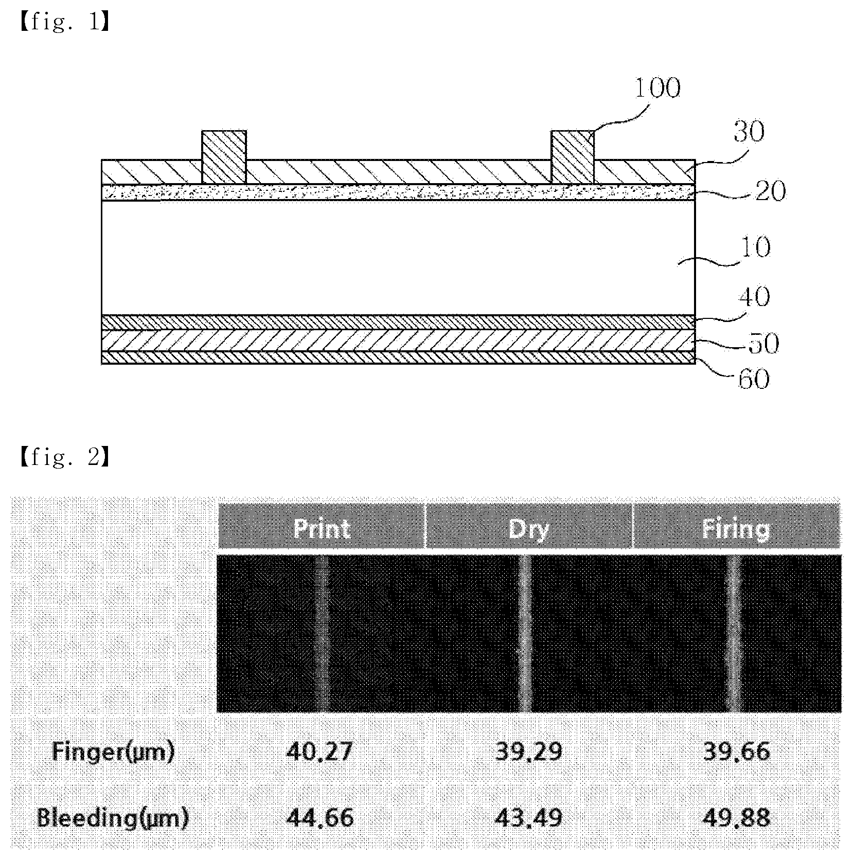
[0005] Conventionally, since the metal paste printed on the front and rear surfaces of the silicon wafer is a flowable composition, as shown in FIG. 2, changes in line width (finger) and residue (bleeding) occur with increased processing time for printing, drying and firing, and consequently, the light-receiving area is reduced, undesirably deteriorating the efficiency of the solar cell.
[0006] Also, in order to increase short-circuit current (Isc), there is a tendency to reduce the line width on a printing mask design to 40 .mu.m, 36 .mu.m, 34 .mu.m and 32 .mu.m, but in the 32 .mu.m line-width design, the reliability of printing quality characteristics is poor and it is difficult to realize an additional line-width reduction.
DISCLOSURE
Technical Problem
[0007] Accordingly, an objective of the present invention is to provide a conductive paste for a solar cell electrode, in which the sintering shrinkage rate of a metal powder thereof may be increased, thus enlarging the light-receiving area of the front electrode of a solar cell formed using the same and increasing short-circuit current (Isc) to thereby enhance the power generation efficiency of the solar cell.
[0008] Another object of the present invention is to provide a conductive paste for a solar cell electrode, in which line resistance may be decreased due to an increase in the sinterability of a metal powder thereof, thus lowering series resistance (Rs) and increasing a fill factor (FF), thereby enhancing the power generation efficiency of the solar cell.
[0009] However, the objectives of the present invention are not limited to the foregoing, and other objectives which are not mentioned herein will be able to be clearly understood by those skilled in the art from the following description.
Technical Solution
[0010] The present invention provides a conductive paste for a solar cell electrode, comprising a metal powder, a glass frit and an organic vehicle, in which the metal powder includes a metal powder having a shrinkage rate of 15 to 30%, measured as an area reduction rate after applying, drying and firing the paste including the metal powder, compared to the state before firing.
[0011] Also, the metal powder may include at least two selected from the group consisting of a first metal powder having a sintering shrinkage rate of 15 to 20%, a second metal powder having a sintering shrinkage rate of 20 to 25%, and a third metal powder having a sintering shrinkage rate of 25 to 30%.
[0012] Also, the metal powder may be configured such that the amount of the metal powder having a relatively high shrinkage rate is greater than the amount of the metal powder having a relatively low shrinkage rate.
[0013] In addition, the present invention provides a solar cell, comprising a front electrode provided on a substrate and a rear electrode provided under the substrate, in which the front electrode is manufactured by applying, drying and firing the conductive paste described above.
ADVANTAGEOUS EFFECTS
[0014] According to the present invention, a conductive paste includes a metal powder having an increased sintering shrinkage rate, and thus the light-receiving area of the front electrode of a solar cell formed using the same can be enlarged and short-circuit current (Isc) can be increased, thereby enhancing the power generation efficiency of the solar cell.
[0015] Also, according to the present invention, line resistance can be decreased due to an increase in the sinterability of the metal powder of the conductive paste, thus lowering series resistance (Rs) and increasing a fill factor (FF), thereby enhancing the power generation efficiency of the solar cell.
DESCRIPTION OF DRAWINGS
[0016] FIG. 1 shows a schematic cross-sectional view of a typical solar cell device; and
[0017] FIG. 2 shows changes in line width and residue during processing upon formation of a conventional solar cell electrode.
MODE FOR INVENTION
[0018] In the following description of the present invention, the terms used herein are merely intended to describe specific embodiments and are not to be construed as limiting the scope of the present invention, which is defined by the appended claims. Unless otherwise defined, all technical or scientific terms used herein have the same meanings as those typically understood by persons having ordinary knowledge in the art to which the present invention belongs.
[0019] Unless otherwise stated, the terms "comprise", "comprises" and "comprising" are used to designate the presence of an object, a step or groups of objects and steps described to in the specification and claims, and should be understood as not excluding the presence or additional possibility of inclusion of any other objects, steps or groups of objects or steps.
[0020] Unless otherwise noted, various embodiments of the present invention may be combined with other embodiments. In particular, any feature that is said to be preferable or favorable may be combined with any other features said to be preferable or favorable. Hereinafter, a description will be given of embodiments of the present invention and effects thereof with reference to the appended drawings.
[0021] An embodiment of the present invention pertains to a paste suitable for use in the formation of a solar cell electrode, particularly a conductive paste including a metal powder having an increased sintering shrinkage rate. More particularly, the conductive paste according to the present invention includes a metal powder, a glass frit, an organic vehicle and an additive.
[0022] The conductive paste according to the present invention includes a metal powder having an increased sintering shrinkage rate, thus enlarging the light-receiving area of the front electrode of a solar cell formed using the same and increasing short-circuit current (Isc) to thereby enhance the power generation efficiency of the solar cell.
[0023] The metal powder may include a silver (Ag) powder, a copper (Cu) powder, a nickel (Ni) powder, and an aluminum (Al) powder, and a silver powder is mainly used for the front electrode and an aluminum powder is mainly used for the rear electrode.
[0024] As the metal powder according to an embodiment of the present invention, a metal powder having a shrinkage rate (%) of 15 to 30% may be used. The shrinkage rate may be measured as an area reduction rate after applying, drying and firing the paste including the metal powder and the binder resin, compared to the state before firing. If the shrinkage rate of the metal powder is less than 15%, the line width may become wide, undesirably decreasing short-circuit current (Isc). On the other hand, if the shrinkage rate to thereof exceeds 30%, contact resistance may increase due to excessive firing, which is undesirable. Preferably, a metal powder having a shrinkage rate of 20 to 30%, and more preferably, a metal powder having a shrinkage rate of 25 to 30%, is used.
[0025] As the metal powder according to another embodiment of the present invention, a first metal powder having a shrinkage rate of 15 to 20% may be used alone, a second metal powder having a shrinkage rate of 20 to 25% may be used alone, or a third metal powder having a shrinkage rate of 25 to 30% may be used alone. Compared to the case in which the first metal powder is used alone, the use of the second metal powder alone is preferable, and compared to the case in which the second metal powder is used alone, the use of the third metal powder alone is further preferable.
[0026] As the metal powder according to still another embodiment of the present invention, a mixture of at least two metal powders having different shrinkage rates may be used. For example, a mixture of the first metal powder and the second metal powder may be used, a mixture of the second metal powder and the third metal powder may be used, or a mixture of the third metal powder and the first metal powder may be used. When a mixture of two metal powders having different shrinkage rates is used, the mixing ratio thereof is not limited, but it is preferred that the amount of the metal powder having a relatively high shrinkage rate be greater than the amount of the metal powder having a relatively low shrinkage rate. Preferably, the second metal powder and the third metal powder are mixed, the amount of the third metal powder that is mixed being 50% or more based on the total amount of the metal powder.
[0027] Alternatively, a mixture comprising all of the first metal powder, the second metal powder and the third metal powder may be used. As such, these powders are mixed such that the amount of the third metal powder is the greatest and the amount of the first metal powder is the smallest.
[0028] A silver powder having a high shrinkage rate of 15 to 30% may be prepared in a wet reduction manner in which silver particles are precipitated by reacting silver nitrate, ammonia, an organic acid alkali metal salt and a reducing agent.
[0029] The amount of the metal powder is 40 to 95 wt % based on the total weight of the conductive paste composition, taking into consideration the thickness and line resistance of an electrode formed upon printing. Preferably, the amount thereof is 60 to 90 wt %.
[0030] When a silver powder is contained in the conductive paste in order to form the front electrode for a solar cell, the silver powder is preferably a pure silver powder, and other examples thereof may include a silver-coated complex powder having a silver layer on at least a surface thereof, an alloy composed mainly of silver, etc. Also, the silver may be used in combination with another metal powder. For example, aluminum, gold, palladium, copper, nickel, and the like may be used.
[0031] The average particle diameter (D50) of the metal powder may range from 0.5 to 5 .mu.m, and preferably 1 to 3 .mu.m considering ease of formation of a paste and density upon firing, and the shape thereof may be at least one of a spherical shape, an acicular shape, a planar shape, and an indeterminate shape. The silver powder may be used in a mixture of two or more powders having different average particle diameters, particle size distributions and shapes.
[0032] The composition, particle diameter and shape of the glass frit are not particularly limited. Not only a lead-containing glass frit but also a lead-free glass frit may be used. As the components and amounts of the glass frit, 5 to 29 mol % of PbO, 20 to 34 mol % of TeO.sub.2, 3 to 20 mol % of Bi.sub.2O.sub.3, 20 mol % or less of SiO.sub.2, and 10 mol % or less of B.sub.2O.sub.3 are preferably used on an oxide basis, and an alkali metal (Li, Na, K, etc.) and an alkaline earth metal (Ca, Mg, etc.) may be contained in an amount of 10 to 20 mol %. When these components are combined in the above amounts, an increase in the line width of the electrode is prevented and superior contact resistance is ensured at high sheet resistance, resulting in superior short-circuit current characteristics.
[0033] Also, the average particle diameter of the glass frit is not particularly limited, but may fall in the range of 0.5 to 10 .mu.m, and the glass frit may be used by mixing a variety of particles having different average particle diameters. Preferably, at least one glass frit has an average particle diameter (D50) of 2 .mu.m to 10 .mu.m. Thereby, reactivity upon firing becomes excellent, and in particular, damage to an n layer at a high temperature may be minimized, adhesion may be enhanced, and superior open voltage (Voc) may result. Moreover, an increase in the line width of the electrode upon firing may be reduced.
[0034] The amount of the glass frit is preferably 1 to 10 wt % based on the total weight of the conductive paste composition. If the amount thereof is less than 1 wt %, incomplete firing may occur, and thus electrical resistivity may increase, which is undesirable. On the other hand, if the amount thereof exceeds 10 wt %, the glass content in the fired body of the silver powder may become too large, and thus electrical resistivity may increase, which is undesirable.
[0035] The organic vehicle is not particularly limited, but may include an organic binder, a solvent, and the like. The solvent may sometimes be omitted. The amount of the organic vehicle is not particularly limited, but is preferably 1 to 30 wt % based on the total weight of the conductive paste composition.
[0036] The organic vehicle is used to maintain the uniformly mixed state of the metal powder and the glass frit. For example, when conductive paste is applied onto a substrate through screen printing, the conductive paste is homogenized, thus suppressing the blur and flow of the printed pattern, and moreover, properties that facilitate discharge of the conductive paste from the screen plate and separation of the plate are obtained.
[0037] The organic binder contained in the organic vehicle is not particularly limited, but examples thereof may include a cellulose ester compound such as cellulose acetate, cellulose acetate butyrate and the like, a cellulose ether compound such as ethyl cellulose, methyl cellulose, hydroxypropyl cellulose, hydroxyethyl cellulose, hydroxypropylmethyl cellulose, hydroxyethylmethyl cellulose and the like, an acrylic compound such as polyacrylamide, polymethacrylate, polymethylmethacrylate, polyethylmethacrylate and the like, and a vinyl compound such as polyvinyl butyral, polyvinyl acetate, polyvinyl alcohol, and the like. At least one of these organic binders may be selected and used.
[0038] As the solvent used for the dilution of the composition, at least one selected from among alpha-terpineol, Texanol, dioctyl phthalate, dibutyl phthalate, cyclohexane, hexane, toluene, benzyl alcohol, dioxane, diethylene glycol, ethylene glycol monobutyl ether, ethylene glycol monobutyl ether acetate, diethylene glycol monobutyl ether, diethylene glycol monobutyl ether acetate, and the like may be used.
[0039] The conductive paste composition according to the present invention may further include, as necessary, a typically known additive, for example, a dispersant, a plasticizer, a viscosity modifier, a surfactant, an oxidizing agent, a metal oxide, a metal organic compound and the like.
[0040] In addition, the present invention pertains to a method of forming an electrode for a solar cell, in which the conductive paste is applied on a substrate, dried and fired, and to a solar cell electrode manufactured by the method. Here, a substrate, a printing process, a drying process and a firing process useful in conventional methods for manufacturing solar cells may be applied, with the exception that the conductive paste including the silver powder having the properties above is used in the method of forming a solar cell electrode according to the present invention. For example, the substrate may be a silicon wafer.
[0041] When an electrode is formed using the conductive paste according to the present invention, a sintering shrinkage rate may be increased even by the use of a printing mask having the same line width, thus enlarging the light-receiving area of the solar cell and increasing short-circuit current (Isc).
[0042] Also, line resistance is decreased due to an increase in the sinterability of the metal powder of the conductive paste composition according to the present invention, thus lowering series resistance (Rs) and increasing a fill factor (FF), thereby enhancing the power generation efficiency of the solar cell.
[0043] Moreover, the conductive paste according to the present invention may be applied to crystalline solar cell (P-type, N-type), PESC (Passivated Emitter Solar Cell), PERC (Passivated Emitter and Rear Cell), and PERL (Passivated Emitter Real Locally Diffused) structures, and also to modified printing processes such as double printing, dual printing, etc.
Examples and Comparative Examples
[0044] A conductive paste was prepared in a manner in which 0.4 g of ethyl cellulose, 2.3 g of Texanol, 2.0 g of DBA, 1.8 g of DB, 0.3 g of amide wax, 0.2 g of DPGDB, 2.0 g of a glass frit and 1.5 g of a dispersant were placed in a mixer, dispersed using a three-roll mill, mixed with a silver powder, further dispersed using a three-roll mill, and then defoamed under reduced pressure. The properties of the silver powder that was used are shown in Table 1 below.
TABLE-US-00001 TABLE 1 Classification D50 (.mu.m) Shrinkage rate (%) Silver powder A 2.1 15~20% Silver powder B 2.18 20~25% Silver powder C 2.06 25~30% Silver powder D 2.5 10~15% Silver powder E 1.7 30~35%
TABLE-US-00002 TABLE 2 Silver Silver Silver Silver Silver No. powder A powder B powder C powder D powder E Example 1 100% Example 2 100% Example 3 100% Example 4 40% 60% Example 5 40% 60% Example 6 60% 40% Example 7 40% 60% Example 8 20% 30% 50% Example 9 50% 30% 20% Comparative 100% Example 1 Comparative 100% Example 2 Comparative 50% 50% Example 3
Test Examples
[0045] (1) Measurement of Sintering Shrinkage Rate
[0046] 1 g of the silver powder of each of Examples and Comparative Examples and 0.15 g of a 10% ethyl cellulose (90% DBA) solution were mixed, and the resultant mixture was applied at a thickness of 200 .mu.m and dried in a convection oven at 80.degree. C. for 3 hr. The dried test sample was cut to a size of 1 mm.times.1 mm and fired in a belt-type IR firing furnace (CF-series, made by Despatch) for a solar cell at a rate of 250 rpm and an actual peak temperature of 780.degree. C., after which the width and length after shrinking were measured and thus the area reduction rate was determined to be a shrinkage rate.
[0047] (2) Measurement of Conversion Efficiency and Resistance
[0048] The conductive paste prepared above was pattern-printed on the front surface of a wafer through a screen-printing process using a 40 .mu.m mesh and dried at 200 to 350.degree. C. for 20 sec to 30 sec using a belt-type drying furnace. Thereafter, an aluminum paste was printed on the rear surface of the wafer and dried in the same manner as above. The cell thus formed was fired at 500 to 900.degree. C. for 20 to 30 sec using a belt-type firing furnace, thereby manufacturing a solar cell.
[0049] The solar cell thus manufactured was measured for conversion efficiency (Eff), short-circuit current (Isc), open voltage (Voc), fill factor (FF), line resistance (Rline) and series resistance (Rs) using a solar cell efficiency measurement device (cetisPV-Celltest 3, made by Halm). The results are shown in Table 3 below.
[0050] The conductive paste of each of Examples 1 to 3 was pattern-printed through a screen-printing process using a 360-16 mesh having therein openings 32 .mu.m in size, and dried and fired in the same manner as above, thus manufacturing a solar cell, which was then measured for conversion efficiency (Eff), short-circuit current (Isc), open voltage (Voc), fill factor (FF), line resistance (Rline) and series resistance (Rs) in the same manner as above. The results are shown in Table 4 below.
TABLE-US-00003 TABLE 3 Isc Voc Eff FF Rs Rline-1 Rline-2 (A) (V) (%) (%) (m.OMEGA.) (.OMEGA.) (.OMEGA.) Example 1 9.437 0.6394 19.610 77.724 2.03 40.17 40.09 Example 2 9.441 0.6393 19.746 78.245 1.826 38.31 36.75 Example 3 9.444 0.6414 19.804 78.187 1.853 38.57 35.70 Example 4 9.4268 0.6399 19.706 78.127 1.94 42.11 39.51 Example 5 9.472 0.6402 19.812 78.14 1.75 38.4 38.4 Example 6 9.4279 0.6397 19.736 78.267 1.79 39.4 42.1 Example 7 9.438 0.64 19.806 78.455 1.8 42.9 39.7 Example 8 9.4285 0.6400 19.727 78.188 1.83 39.37 39.02 Example 9 9.438 0.6399 19.760 78.25 1.81 39.6 37.9 Comparative 9.3941 0.6383 19.631 78.297 1.77 41.12 40.22 Example 1 Comparative 9.476 0.6385 19.504 77.09 2.19 38.00 36.22 Example 2 Comparative 9.4119 0.6383 19.708 78.453 1.70 38.95 38.44 Example 3
TABLE-US-00004 TABLE 4 Isc Voc Eff FF Rs Rline-1 Rline-2 (A) (V) (%) (%) (m.OMEGA.) (.OMEGA.) (.OMEGA.) Example 1 9.401 0.6382 19.707 78.556 1.637 33.22 33.37 Example 2 9.416 0.6383 19.761 78.635 1.625 33.00 33.11 Example 3 9.429 0.6387 19.807 78.651 1.568 31.86 32.44
[0051] Given that the efficiency of a solar cell is measured in 0.2% increments and an increase in efficiency of 0.2% is very meaningful, as shown in Table 3, the solar cell including the electrode made of the conductive paste including the metal powder having a shrinkage rate (%) of 15 to 30% according to the present invention was high in short-circuit current compared to Comparative Example 1 including the metal powder having a shrinkage rate of 15% or less, and was low in series resistance compared to Comparative Example 2 including the metal powder having a shrinkage rate of 30% or more, thus exhibiting high conversion efficiency, resulting in increased power generation efficiency of the solar cell.
[0052] Also, short-circuit current and conversion efficiency were higher in Examples 4 to 9 using the mixtures of two or more metal powders having different shrinkage rates than in Examples 1 to 3 using the metal powder alone, and moreover, short-circuit current and conversion efficiency were higher in Examples 5 and 8, in which the metal powder having a high shrinkage rate was mixed in a larger amount, than in Examples 6 and 9, in which the metal powder having a low shrinkage rate was mixed in a larger amount, thereby exhibiting superior power generation efficiency of a solar cell.
[0053] Furthermore, as shown in Table 4, sufficient short-circuit current was confirmed to be ensured even at a wide line width of 40 .mu.m compared to the case in which a fine line width of 32 .mu.m was formed using the conductive paste according to the present invention.
[0054] The features, structures, effects and the like illustrated in the individual exemplary embodiments above may be combined or modified with other exemplary embodiments by those skilled in the art. Therefore, content related to such combinations or modifications should be understood to fall within the scope of the present invention.
* * * * *
D00000
D00001
XML
uspto.report is an independent third-party trademark research tool that is not affiliated, endorsed, or sponsored by the United States Patent and Trademark Office (USPTO) or any other governmental organization. The information provided by uspto.report is based on publicly available data at the time of writing and is intended for informational purposes only.
While we strive to provide accurate and up-to-date information, we do not guarantee the accuracy, completeness, reliability, or suitability of the information displayed on this site. The use of this site is at your own risk. Any reliance you place on such information is therefore strictly at your own risk.
All official trademark data, including owner information, should be verified by visiting the official USPTO website at www.uspto.gov. This site is not intended to replace professional legal advice and should not be used as a substitute for consulting with a legal professional who is knowledgeable about trademark law.