All Silicon Broadband Ultra-violet Metasurfaces
Deng; Yang ; et al.
U.S. patent application number 16/506043 was filed with the patent office on 2020-01-16 for all silicon broadband ultra-violet metasurfaces. The applicant listed for this patent is THE REGENTS OF THE UNIVERSITY OF CALIFORNIA. Invention is credited to Yang Deng, Zilun Gong, Xi Wang, Jie Yao.
| Application Number | 20200018871 16/506043 |
| Document ID | / |
| Family ID | 69139125 |
| Filed Date | 2020-01-16 |


| United States Patent Application | 20200018871 |
| Kind Code | A1 |
| Deng; Yang ; et al. | January 16, 2020 |
ALL SILICON BROADBAND ULTRA-VIOLET METASURFACES
Abstract
A device has a substrate transparent to ultraviolet (UV) light, and at least one metalens formed of a material having large permittivity of UV light on the substrate. A device has a UV reflector, a UV transparent film on the reflector, and at least one metalens formed of a material having large permittivity of UV light on the film.
| Inventors: | Deng; Yang; (Fremont, CA) ; Wang; Xi; (Newark, DE) ; Gong; Zilun; (Berkelely, CA) ; Yao; Jie; (Fremont, CA) | ||||||||||
| Applicant: |
|
||||||||||
|---|---|---|---|---|---|---|---|---|---|---|---|
| Family ID: | 69139125 | ||||||||||
| Appl. No.: | 16/506043 | ||||||||||
| Filed: | July 9, 2019 |
Related U.S. Patent Documents
| Application Number | Filing Date | Patent Number | ||
|---|---|---|---|---|
| 62697914 | Jul 13, 2018 | |||
| Current U.S. Class: | 1/1 |
| Current CPC Class: | G02B 1/002 20130101; G02B 1/041 20130101; G02B 1/10 20130101; G02B 5/283 20130101 |
| International Class: | G02B 1/00 20060101 G02B001/00; G02B 1/10 20060101 G02B001/10; G02B 1/04 20060101 G02B001/04; G02B 5/28 20060101 G02B005/28 |
Goverment Interests
STATEMENT REGARDING FEDERALLY SPONSORED RESEARCH AND DEVELOPMENT
[0002] This invention was made with government support under Grant Number 1555336 awarded by the National Science Foundation. The government has certain rights in the invention.
Claims
1. A device, comprising: a substrate transparent to ultraviolet (UV) light; and at least one metalens formed of a material having a permittivity of UV light of at least 10 on the substrate.
2. The device of claim 1, wherein the at least one metalens comprises a single bar structure.
3. The device of claim 1, wherein the at least one metalens comprises a double bar structure.
4. The device of claim 1, wherein the substrate comprises quartz.
5. The device of claim 1, wherein the material having the permittivity of UV light of at least 10 comprises one of a material selected from a group consisting of: silicon, silicon dioxide, and silicon carbide.
6. The device of claim 4, wherein the material having the permittivity of UV light of at least 10 comprises a silicon-based material such that the entire device is comprised of silicon-based materials.
7. A device, comprising: an ultraviolet (UV) light reflector; a UV transparent film on the reflector; and at least one metalens formed of a material having a permittivity of UV light of at least 10 on the UV transparent film.
8. The device of claim 7, wherein the at least one metalens comprises a single bar structure.
9. The device of claim 7, wherein the at least one metalens comprises a double bar structure.
10. The device of claim 7, wherein the substrate comprises quartz.
11. The device of claim 7, wherein the material having the permittivity of UV light of at least 10 comprises one of a material selected from a group consisting of: silicon, silicon dioxide, and silicon carbide.
12. The device of claim 10, wherein the material having the permittivity of UV of at least 10 light comprises a silicon-based material such that the entire device is comprised of silicon-based materials.
13. A method of forming a metasurface, comprising: forming at least one layer of silicon on a UV responsive substrate; selectively removing portions of the at least one layer of silicon to form voids between remaining portions of the at least one layer of silicon on the UV responsive substrate, wherein the remaining portions form metalens antenna structures.
14. The method as claimed in claim 13, wherein forming at least one layer of silicon on a UV responsive substrate comprises: forming a single silicon layer as the at least one layer of silicon on an insulator formed on a substrate to produce a silicon on insulator (SOI) device; placing the SOI device on a UV responsive substrate comprised of a UV-transparent, silicon-based substrate such that the single silicon layer of the SOI device is in contact with the UV-transparent, silicon-based substrate; removing the substrate and the insulator to leave only the single silicon layer on the UV-transparent, silicon-based substrate.
15. The method as claimed in claim 14, further comprising: forming a layer of resist on the single silicon layer; patterning the resist to protect portions of the single silicon layer; etching the resist to remove other portions of the at least one layer of silicon to form voids, such that the protected portions form metalens structures; and removing any remaining resist from the metalens structures.
16. The method as claimed in claim 14, further comprising: depositing a first insulator layer on the at least one layer of silicon, wherein the at least one layer of silicon comprises two layers of silicon and the insulator is deposited on the first layer of silicon; and bonding a second SOI wafer to the first insulator layer, the second SOI wafer having a second silicon layer on a second insulator layer, the second insulator layer being on a second silicon substrate.
17. The method as claimed in claim 16, further comprising: removing the second silicon substrate and the second insulator layer; depositing a layer of resist on the second silicon layer; patterning and removing portions of the layer of resist to leave areas of resist and voids; removing portions of the first and second silicon layers and the first insulator layer, leaving structures comprising stacks of the first silicon layer, the first insulator layer and the second silicon layer as double bar metalens structures; removing any remaining portions of resist.
18. The method as claimed in claim 13, wherein the UV responsive substrate comprises a UV reflective substrate.
19. The method as claimed in claim 18, wherein the method further comprise depositing a layer of UV transparent material on the UV reflective substrate.
Description
CROSS REFERENCE TO RELATED APPLICATION
[0001] This application claims priority to and the benefit of U.S. Provisional Application No. 62/697,914 filed Jul. 13, 2018, which is incorporated herein by reference in its entirety.
BACKGROUND
[0003] Conventional ultraviolet (UV) lenses rely on manipulating the optical phase by changing the thickness of UV transparent materials to generate different optical paths from the center to the edge of the lens. These lenses typically consist of UV transparent materials and are robust. However, compactly integrated systems cannot include these traditional lenses with macroscopic thicknesses. Additionally, most of the widely used materials such as MgF.sub.2, and CaF.sub.2, lack compatibility with CMOS processes.
BRIEF DESCRIPTION OF THE DRAWINGS
[0004] FIGS. 1A-1D shows a circuit model for lossy dielectric nanorod and calculated scattering efficiency comparison between different materials.
[0005] FIG. 2 shows an example of beam steering using metasurfaces.
[0006] FIG. 3 shows an example of beam focusing using metasurfaces.
[0007] FIG. 4 shows a ray tracing diagram of a focused beam in a focused hologram.
[0008] FIG. 5 shows a schematic of a focused UV hologram for lithography.
[0009] FIG. 6 shows a graph of calculated and measured conversion and diffraction efficiencies for an embodiment of a single-bar metasurface.
[0010] FIG. 7 shows a graph of calculated and measured conversion and diffraction efficiencies for an embodiment of a double-bar metasurface.
[0011] FIG. 8 shows a graph of calculated conversion efficiency for an embodiment of a reflective metasurface with a single-bar structure.
[0012] FIGS. 9-15 show an embodiment of a process of manufacturing embodiments of a single bar metasurface.
[0013] FIGS. 16-22 show an embodiment of a process of manufacturing an embodiment of a double bar metasurface.
DETAILED DESCRIPTION OF THE EMBODIMENTS
[0014] The embodiments here provide a new platform for building all-silicon (Si) metasurfaces in the ultraviolet (UV) range with thicknesses smaller than the working wavelength to manipulate broadband UV light with efficiencies higher than 10%. Other than silicon, indications are that other materials with large permittivity in the UV range, such as many oxides, nitrides and carbides, may also make good candidates for metasurface devices in the UV realm. Examples include, but are not limited to, silicon dioxide (SiO.sub.2) and silicon carbide (SiC). Large permittivity in the UV range is related to strong absorption in the UV range, and as used here means materials with a large imaginary part of permittivity and therefore an associated large, real part of permittivity. Large as used here means any value greater than 10.
[0015] A `metasurface` as used here consists of a surface of a metamaterial, which is a flat optical device that exhibits special properties as a consequence of the metamaterial's structure at the microscopic or macroscopic level. In the embodiments here, the metamaterial consists of silicon or other materials with large permittivity in the UV range. One should note that while the discussion and examples here focus on silicon, no limitation to silicon is intended nor should any be implied.
[0016] The embodiments here rely upon a widely utilized and CMOS (complementary metal oxide semiconductor) compatible material, silicon, and the working wavelength covers from 290 nanometers (nm) to 410 nm, which can be further extended with materials beyond silicon. One application of these embodiments lies in thin metalenses for high-resolution imaging and lithography in the UV range.
[0017] An all-Si metalens overcomes the limitations of conventional lenses and allows ready integration and fabrication on a chip with common CMOS technologies in industry. This leads to cost-effective and massive, or large-scale, fabrication. The ultra-compact and easy to manufacture metalenses apply to both regular optical setups and integrated photonic circuits. The thinness of the metalens makes it suitable for general imaging systems, such as smart phone cameras with significantly reduced device thickness. The UV signature of these lenses enables its use as possible replacements in traditional projection lenses in high-resolution lithography stepper machinery.
[0018] FIG. 1 shows a circuit model for a lossy dielectric nanorod and calculated scattering efficiency comparison between different materials. FIG. 1A shows a schematic configuration of a nanorod and scattering field. One should note that the circuit model calculation does not include a substrate. FIG. 1B shows color mapping of scattering efficiency of a nanorod as a function of Re(.epsilon.) (.epsilon..sub.r) and lm(.epsilon.) (.epsilon..sub.i), with L equaling 130 nm, W=30 nm, and H=30 nm at the wavelength of 380 nm. FIG. 1C shows a circuit model for a single antenna or `bar.` FIG. 1D shows R.sub.rad, |Z.sub.tot|, and R.sub.rad/|Z.sub.tot| plotted as a function of .epsilon..sub.i when .epsilon..sub.r is fixed at 10, where R.sub.rad is the radiation resistance, and Z.sub.tot is the total impedance.
[0019] FIG. 1A depicts a single unit of the metasurface in which the environment is air. The scattering efficiency (SE) of a nanorod consisting of a material with arbitrary permittivities of FIG. 1A is investigated. FIG. 1B plots color contour of the SE of a nanorod as a function of the .epsilon..sub.r and .epsilon..sub.i at 380 nm. This shows that not only .epsilon..sub.r but also .epsilon..sub.i contribute positively to the SE in a dissipative system. Hence, single crystal Si is chosen as the material platform for efficient metasurfaces, due to its large permittivity at UV frequencies, CMOS compatibility and mature fabrication technologies. FIG. 1C shows the circuit model constructed to calculate the SE of a nanorod [M. Eggleston, K. Messer, L. Zhang, E. Yablonovitch, M. Wu, Proc. Nall. Acad. Sci. 2015, 112, 1704.]. The circuit contains an AC voltage source (V.sub.0) modeling the incident plane wave. The total impedance, Z.sub.tot of a nano-antenna includes radiation resistance (R.sub.rad), self-inductance in the rod (L.sub.f), Ohmic resistance (R.sub..OMEGA.) and self-capacitance (C.sub.self) in dielectric materials. The R.sub.rad is independent of material permittivities; the energy "lost" to R.sub.rad is the scattered energy. FIG. 1D indicates that increasing .epsilon..sub.i reduces |Z.sub.tot| of the circuit while R.sub.rad, is a constant, resulting in increasing scattering energy ratio. This allows the embodiments to utilize common lossy dielectrics such as Si to realize metasurfaces over a broad range, including the UV region.
[0020] FIGS. 2-3 show two functionalities achievable by this metasurface: beam steering as shown in FIG. 2 and focusing in FIG. 3. Among metasurface designs, the scatterer-orientation-controlled geometric phase (Pancharatnam-Berry phase) approach has been widely utilized to manipulate the phase of the scattered field for circularly polarized light [M. V. Berry, J. Mod. Opt. 1987, 34, 1401; and S. Pancharatnam, Proceedings of the Indian Academy of Sciences, Section A, Springer, 1956, 44, 398.] The embodiments here use the same approach of a nanorod-shaped scatterer to control the phase of the scattered light with opposite helicity by only changing the orientation angle of the scatterer. The phase is not subjected to variations in size and material properties, upon which the scattering efficiency is dependent [D. Lin, P. Fan, E. Hasman, M. L. Brongersma, Science 2014, 345, 298.; M. Khorasaninejad, W. T. Chen, R. C. Devlin, J. Oh, A. Y. Zhu, F. Capasso, Science 2016, 352, 1190.; and G. Zheng, H. Muhlenbemd, M. Kenney, G. Li, T. Zentgraf, S. Zhang, Nat. Nanotechnol. 2015, 10, 308.]. This unique feature allows the embodiments to have great freedom in optimizing the efficiency of the nanoantennas without sacrificing the phase control.
[0021] In addition, the embodiments may combine a metalens design and hologram phase distribution to form a focused pattern as shown in the ray tracing diagram of FIG. 4, and a schematic of a focused UV hologram for lithography in FIG. 5. This may find a plethora of applications in projection lenses for maskless lithography steppers, where the mask information is encoded into the metalens.
[0022] FIG. 6 shows a plot of the conversion efficiency of the metasurfaces, the ratio of the power of the converted beam to the total incident power, and the diffraction efficiency, the ratio of the power of the converted beam to the direct transmitted power for a single bar embodiment. Over a broadband range from 290 nm to 410 nm, the conversion efficiency reaches as high as 15% at 380 nm and remains at the level of 10% even at the short wavelength of 290 nm. The diffraction efficiency achieves 30% around 380 nm and maintains over 15% at shorter wavelengths. The experimental results in FIG. 6 agree with circuit model calculations.
[0023] FIG. 7 shows a double bar embodiment, which increases the efficiency of the all-Si metasurface to a diffraction efficiency of 200% and a conversion efficiency of 37% in the transmission mode. This high diffraction efficiency will be essential to improve the signal-to-noise ratio in the far field transmission. The demonstration of effective UV beam steering successfully confirms the proposed mechanism that engineering material property improves the scattering efficiency due to the strong interaction between Si and UV light. Furthermore, the results also indicate that any material that has large permittivity, either real or imaginary part, in the UV range may also form effective UV metasurface devices.
[0024] The discussion so far has focused on devices working in the transmission mode. FIG. 8 shows the simulated conversion efficiency of an embodiment of a reflective metasurface with a single-bar structure. The reflector can be either Aluminum or UV Bragg reflector. The spacer layer is around 30 nm thick, which is UV transparent. The overall conversion efficiency goes beyond 40% and the maximum efficiency reaches 70%. This reflection mode can be combined with either single-bar or double-bar designs.
[0025] FIGS. 9-15, for a single bar embodiment, and FIGS. 16-25, for a double bar embodiment, show an embodiment of a method to massively and cost-effectively fabricate metalenses and metasurfaces for hologram applications. One should note that these figures set out one embodiment of manufacturing processes and other manufacturing processes may be used to achieve the final results.
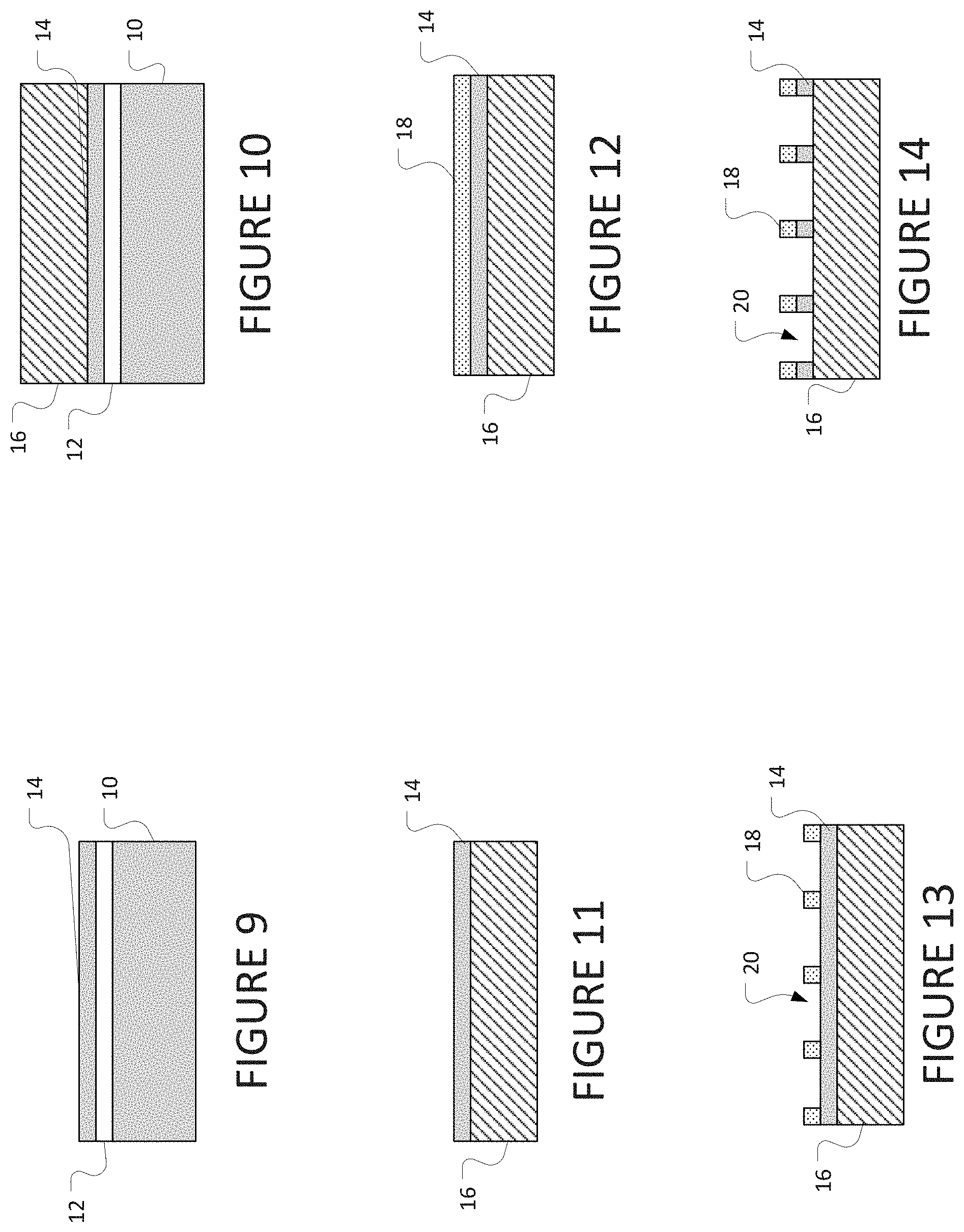
[0026] FIGS. 9-11 show the initial process that can form either a single bar or a double bar structure, with a silicon on insulator (SOI) substrate with device layer thickness of .about.35 nm. The SOI device has a layer of Si 14 on an insulator 12, such as SiO.sub.2, on a Si substrate 10. The process places the device layer face down, on a UV-transparent substrate 16, such as quartz, another silicon based material (SiO.sub.2) and bonded to it at a high pressure. The backside of SOI wafer, the Si substrate 10 is removed. In one embodiment the removal occurs with the combination of mechanical polishing and chemical etching. The oxide layer 12 is etched away with hydrogen fluoride. At this point the two processes diverge.
[0027] FIGS. 12-15 show the remaining process for single-layer Si devices. FIG. 12 shows deposition of a layer of photoresist 18, such as by spin-coating. This layer then undergoes patterning in FIG. 13 to form a pattern of areas of resist 18 and voids such as 20. The silicon layer 14 then undergoes etching to form a pattern of areas of silicon 14 and resist 18, and the voids such as 20 have become deeper, in FIG. 14. In FIG. 15, the resist has been removed, leaving single bar, nanorod antennas formed form silicon layer 14 on the UV transparent substrate 16.
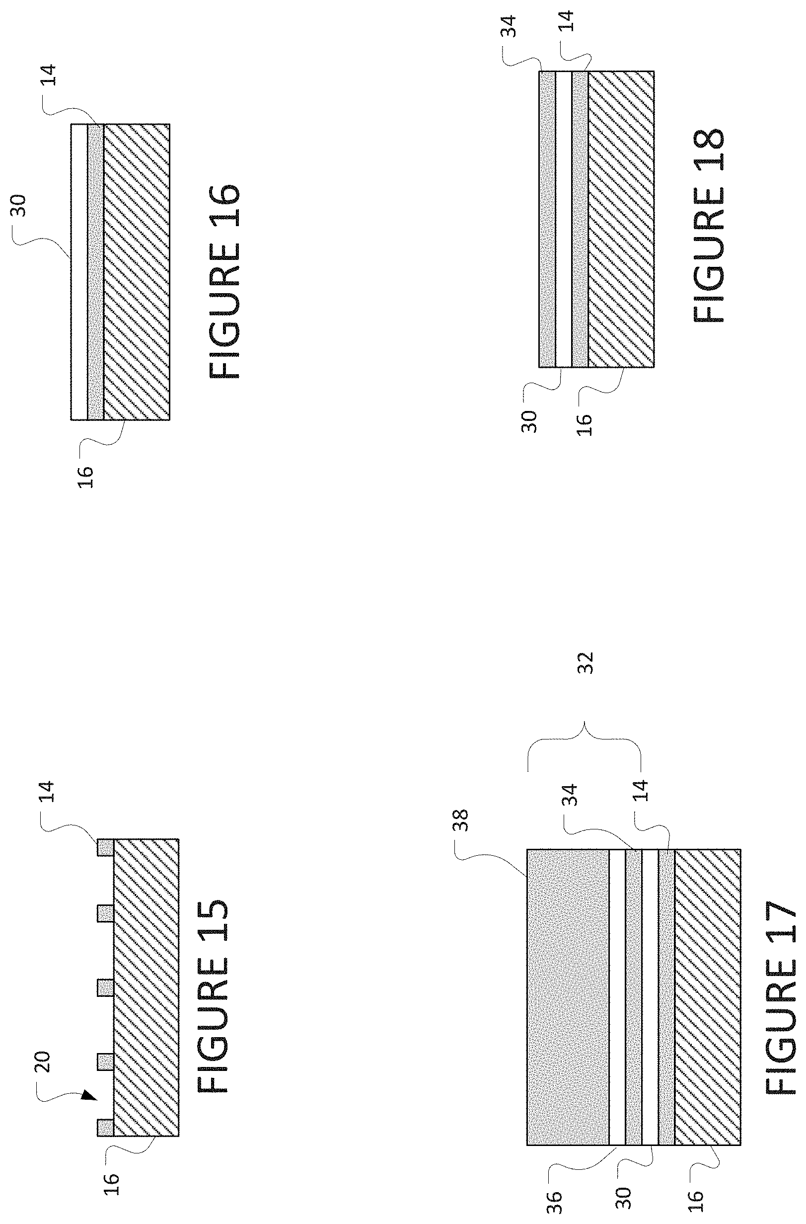
[0028] Turning to the double bar embodiments after the common process between the two, FIG. 16 shows a layer of insulator 30 deposited on the silicon layer 14. Another SOI wafer 32 is then wafer bonded to the insulator layer 30 in FIG. 17. The SOI wafer 32 has a silicon layer 34 on an insulator layer 36, on the silicon substrate 38. The silicon wafer 38 and the insulator layer 36 are removed in accordance with the processes above, or other processes of removal, in FIG. 18. The double stacked device then receives a layer of resist 40 in FIG. 19. The layer of resist undergoes patterning and removal in FIG. 20, leaving areas of resist 40 and voids such as 42. In FIG. 21, the silicon layers 34 and 14, and the insulator 30, are etched. This results in the final pattern of double bar antenna shown in FIG. 21, still with the layer of resist. FIG. 22 shows the final result of a set of double bar antenna.
[0029] In summary, the single and double bar embodiments both consist of forming at least one silicon layer on the UV transparent substrate and then patterning and etching the at least one silicon layer to form nanorod antennas, either single or double bar.
[0030] Regarding the massive fabrication of the reflective metasurfaces, only replacement of UV transparent substrate with UV reflective substrate and deposition of .about.30 nm thick UV transparent material, such as SiO.sub.2, are required. As used here, the term "UV responsive" means that a material is either UV reflective or UV transparent.
[0031] In this manner, one can provide an all-Si metasurface usable as a UV lens, with a thickness much less than conventional lenses. The lenses have high diffraction efficiency and conversion efficiency and are easy to manufacture relative to conventional lenses. In addition, other materials with large permittivity of UV light may also be used. Both transmission or reflection modes can be designed and fabricated for specific applications.
[0032] It will be appreciated that variants of the above-disclosed and other features and functions, or alternatives thereof, may be combined into many other different systems or applications. Various presently unforeseen or unanticipated alternatives, modifications, variations, or improvements therein may be subsequently made by those skilled in the art which are also intended to be encompassed by the following claims.
* * * * *
D00000
D00001
D00002
D00003
D00004
D00005
D00006
D00007
D00008
XML
uspto.report is an independent third-party trademark research tool that is not affiliated, endorsed, or sponsored by the United States Patent and Trademark Office (USPTO) or any other governmental organization. The information provided by uspto.report is based on publicly available data at the time of writing and is intended for informational purposes only.
While we strive to provide accurate and up-to-date information, we do not guarantee the accuracy, completeness, reliability, or suitability of the information displayed on this site. The use of this site is at your own risk. Any reliance you place on such information is therefore strictly at your own risk.
All official trademark data, including owner information, should be verified by visiting the official USPTO website at www.uspto.gov. This site is not intended to replace professional legal advice and should not be used as a substitute for consulting with a legal professional who is knowledgeable about trademark law.