Housing Contacting System Of A Control Device
Mueller; Elena ; et al.
U.S. patent application number 16/332581 was filed with the patent office on 2020-01-09 for housing contacting system of a control device. The applicant listed for this patent is KNORR-BREMSE SYSTEME FUER NUTZFAHRZEUGE GMBH. Invention is credited to Norbert Behrendt, Klaus Lechner, Elena Mueller, Karin Pohley.
| Application Number | 20200015371 16/332581 |
| Document ID | / |
| Family ID | 59955542 |
| Filed Date | 2020-01-09 |


| United States Patent Application | 20200015371 |
| Kind Code | A1 |
| Mueller; Elena ; et al. | January 9, 2020 |
HOUSING CONTACTING SYSTEM OF A CONTROL DEVICE
Abstract
A housing contacting system of a control device, including: a housing cover and a base element which together define an interior of the control device; a printed circuit board having a front side and a rear side, wherein a conductive surface layer is formed on the rear side and the printed circuit board is arranged in the interior; and a spring element which is at least partially electrically conductive and is arranged between the conductive surface layer and the base element under spring prestress in order to implement rear-side contacting of the printed circuit board. Also described are a related brake control device, a utility vehicle, and a method.
| Inventors: | Mueller; Elena; (Nuernberg, DE) ; Behrendt; Norbert; (Stein, DE) ; Lechner; Klaus; (Pretzfeld, DE) ; Pohley; Karin; (Nuernberg, DE) | ||||||||||
| Applicant: |
|
||||||||||
|---|---|---|---|---|---|---|---|---|---|---|---|
| Family ID: | 59955542 | ||||||||||
| Appl. No.: | 16/332581 | ||||||||||
| Filed: | September 13, 2017 | ||||||||||
| PCT Filed: | September 13, 2017 | ||||||||||
| PCT NO: | PCT/EP2017/073003 | ||||||||||
| 371 Date: | March 12, 2019 |
| Current U.S. Class: | 1/1 |
| Current CPC Class: | H05K 1/0215 20130101; H05K 9/0039 20130101; H05K 1/0216 20130101; H05K 9/0086 20130101; H05K 5/0069 20130101; H05K 2201/10371 20130101; H05K 7/2049 20130101; H05K 2201/10265 20130101 |
| International Class: | H05K 5/00 20060101 H05K005/00; H05K 9/00 20060101 H05K009/00; H05K 1/02 20060101 H05K001/02; H05K 7/20 20060101 H05K007/20 |
Foreign Application Data
| Date | Code | Application Number |
|---|---|---|
| Sep 15, 2016 | DE | 10 2016 117 331.2 |
Claims
1-9. (canceled)
10. A housing contacting system of a control device, comprising: a housing cover and a base element which together define an interior of the control device; a printed circuit board having a front side and a rear side, wherein a conductive surface layer is formed on the rear side and the printed circuit board is arranged in the interior; and a spring element which is at least partially electrically conductive and is arranged between the conductive surface layer and the base element under spring prestress in order to implement rear-side contacting of the printed circuit board.
11. The housing contacting system of claim 10, wherein the housing cover contains a plastic material and the base element contains a metal or a cast material.
12. The housing contacting system of claim 10, wherein the rear-side contacting of the printed circuit board forms EMC contacting or ground contact.
13. The housing contacting system of claim 10, wherein the printed circuit board has a tin-plated surface as surface layer.
14. The housing contacting system of claim 10, wherein the spring element is fastened to a rear side of the printed circuit board and rests on the base element under spring prestress.
15. The housing contacting system of claim 10, wherein the spring element has a leaf spring or a helical spring, and the printed circuit board or the base element has a fastening system for the spring element, and wherein the fastening prevents lateral displacement parallel to the printed circuit board.
16. A brake control device, comprising: a housing contacting system of a control device, including: a housing cover and a base element which together define an interior of the control device; a printed circuit board having a front side and a rear side, wherein a conductive surface layer is formed on the rear side and the printed circuit board is arranged in the interior; and a spring element which is at least partially electrically conductive and is arranged between the conductive surface layer and the base element under spring prestress in order to implement rear-side contacting of the printed circuit board.
17. A utility vehicle, comprising: a brake control device, having a housing contacting system of a control device, including: a housing cover and a base element which together define an interior of the control device; a printed circuit board having a front side and a rear side, wherein a conductive surface layer is formed on the rear side and the printed circuit board is arranged in the interior; and a spring element which is at least partially electrically conductive and is arranged between the conductive surface layer and the base element under spring prestress in order to implement rear-side contacting of the printed circuit board.
18. A method for EMC contacting a printed circuit board in a control device, the method comprising: providing a housing cover and a base element which, when put together, define an interior of the control device; arranging a printed circuit board in the interior, wherein the printed circuit board has a rear side with a conductive surface layer and has a front side; and forming rear-side contacting of the printed circuit board by a spring element which is at least partially electrically conductive and is arranged between the conductive surface layer and the base plate under spring prestress.
Description
FIELD OF THE INVENTION
[0001] The present invention relates to a housing contacting system of a control device and, in particular, to an EMC contacting system (EMC=electromagnetic compatibility) in a plastic housing.
BACKGROUND INFORMATION
[0002] Control devices often fulfil safety-related functions in vehicles. Problem-free functioning of the electronic components in the control devices is therefore important. When the control devices are accommodated in plastic housings, electromagnetic interference signals can directly enter the interior and reach the electronic components. The electronic components are arranged, for example, on a printed circuit board and the intended EMC contacting (for example by adequate ground contact, shielding, etc.) is intended to prevent the electronic components being negatively affected by the electromagnetic interference signal. Therefore, reliable EMC contacting is very important for problem-free functioning of the control device.
[0003] One problem in vehicles is, however, that frequent changes in temperature and vibrations can lead to electrical contacts and, in particular, the EMC contacting system possibly becoming detached or loose over a relatively long period of time and a loose contact being produced. In conventional control devices, direct contacting of the exemplary printed circuit board is performed by a screw connection on a metal sheet which serves, for example, for fastening the control device. A screw connection of this kind can become detached over time due to changes in temperature and vibrations and is often not reliable in the long term. There is therefore a need for alternative solutions in order to ensure reliable contacting of the electronic components in the control device, in particular when used in vehicles.
SUMMARY OF THE INVENTION
[0004] The abovementioned problems are solved by a housing contacting system as described herein, a brake control device as described herein, a utility vehicle as described herein or a contacting method as described herein. Further descriptions herein relate to advantageous developments of the housing contacting system as further described herein.
[0005] The present invention relates to a housing contacting system of a control device which is suitable for use in vehicles, in particular utility vehicles. The housing contacting system comprises a housing cover and a base element which together define an interior in which a printed circuit board having a front side and a rear side is arranged, wherein a conductive surface layer is formed on the rear side. The housing contacting system further comprises a spring element which is at least partially electrically conductive and is arranged between the conductive surface layer and the base plate under (spring) prestress in order to contact the rear side of printed circuit board.
[0006] The housing cover is intended to comprise all housing sections which, apart from a base element, form the housing of the control device. Without limiting the invention to what follows, the housing cover can have, for example, a pot-like shape which is fitted onto the base element in order to protect the electronic components which are arranged in the interior. The front side and the rear side of the printed circuit board define, for example, two opposite sides of the printed circuit board, wherein the front side can be defined, for example, in that the electronic components are fitted onto the printed circuit board from this side and the rear side comprises the corresponding contacting structures between the individual electronic components. However, the front side and rear side can also be defined in a different way, for example at least some of the electronic components can be fitted onto the printed circuit board from the rear side. The exact position of the electronic components is not important for the subject matter of the present invention, but rather the rear side should be defined merely in that EMC contacting (or else ground contacting) is possible, but is not absolutely necessary, from this side.
[0007] In further exemplary embodiments, the housing cover contains a plastic material and the base element contains a metal or a cast material.
[0008] In further exemplary embodiments, the rear-side contacting of the printed circuit board forms EMC contacting or ground contact.
[0009] In further exemplary embodiments, the printed circuit board comprises a tin-plated surface as surface layer, which tin-plated surface can be formed partially or over the full surface area of the rear side
[0010] The spring element can optionally be fastened to the rear side of the printed circuit board and rest on the base element under spring prestress. The spring element can have, for example, a leaf spring or a helical spring. The printed circuit board or the base element can have a fastening system for the spring element, wherein the fastening prevents lateral displacement parallel to the printed circuit board on its rear side. However, movement perpendicular to the printed circuit board may be possible since the spring force acts in this direction and ensures spring stress between the printed circuit board and the base element for fixing purposes. However, it can optionally also be fixed in this direction.
[0011] The present invention also relates to a brake control device comprising a housing contacting system as has been described above. The present invention also relates to a utility vehicle comprising the brake control device.
[0012] Therefore, the exemplary embodiments solve said technical problems in that a spring contact is provided, which spring contact connects a base element to one side of the printed circuit board and the spring force ensures permanent contacting, even in the event of changes in temperature or vibrations.
[0013] In contrast to conventional housing contacting systems in which the printed circuit board is directly contacted, for example, on the base element by a screw, exemplary embodiments have the following advantages: a simple and cost-effective design is rendered possible, the printed circuit board can be screwed into a plastic housing, wherein the spring action always ensures that there is electrical contact between the printed circuit board and the base element. Therefore, tolerances do not need to be taken into account since the spring force automatically equalizes differences between the distance between the base element and the printed circuit board.
[0014] The exemplary embodiments of the present invention will be better understood together with the following detailed description and the accompanying drawings of the different exemplary embodiments which, however, are not intended to be understood such that they limit the disclosure to the specified embodiments, but rather serve merely for explanation and understanding.
BRIEF DESCRIPTION OF THE DRAWINGS
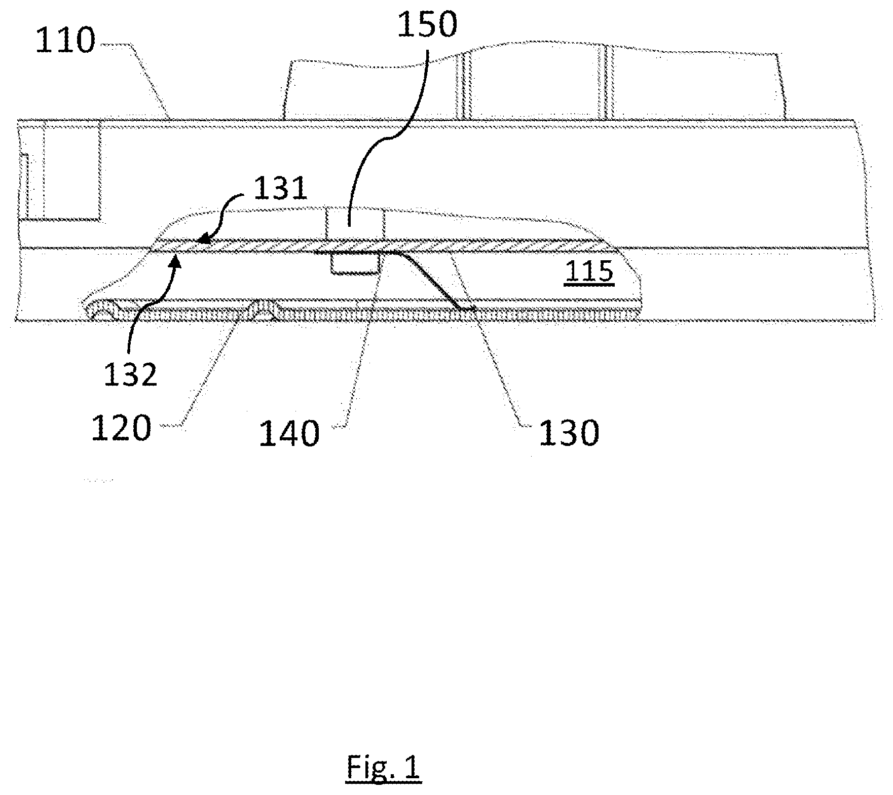
[0015] FIG. 1 shows a housing for a control device comprising a housing contacting system as claimed in an exemplary embodiment of the present invention.
[0016] FIG. 2 shows a flowchart for a method for establishing EMC contacting in a plastic housing.
DETAILED DESCRIPTION
[0017] FIG. 1 shows a housing comprising a housing contacting system according to an exemplary embodiment of the present invention. The housing is suitable for a control device of a vehicle and comprises a housing cover 110, a base element 120 and a printed circuit board 130 having a front side 131 and a rear side 132. The housing cover 110 and the base element 120 define an interior 115 in which the printed circuit board 130 is arranged. The printed circuit board 130 can be fixed to the housing cover 110, for example, by a holding element 150. A spring contact is formed between the rear side 132 of the printed circuit board 130 and the base element 120 by a spring element 140. The spring element 140 can comprise, for example, a leaf spring which is fixed to a rear side 132 of the printed circuit board 130 and exerts a spring force onto the base element 120, without the spring element 140 having to be fastened to the base element 120. It only needs to rest on said base element. For example, the spring element 140 can be fastened to the printed circuit board 130 in such a way that lateral displacement parallel to the printed circuit board 130 is not possible--but the spring element 140 can be removed from the printed circuit board 130 in a perpendicular direction (for example when the base element 120 is removed) (no fixing of the spring element 140 perpendicular to the printed circuit board).
[0018] It is optionally likewise possible for the spring element 140 to be fixed on the base element 120 at least in respect of lateral movement parallel to the printed circuit board and to rest loosely on a rear side 132 of the printed circuit board 130 (that is to say reversal of the abovementioned arrangement). In addition, the spring element 140 can optionally be fastened fixedly to the rear side 132 of the printed circuit board 130 or fixedly on the base element 120 (for example can be soldered or screwed or riveted to/on it).
[0019] In addition, the spring element 140 can be configured as a leaf spring or else as a helical spring. However, the present invention is not limited to specific springs. Rather, other types of spring can also be used, provided that they create prestress between the base element 120 and the printed circuit board 130. The rear side and front side 131, 132 of the printed circuit board 130 can also be interchanged. For example, to this end, the holding element 140 can contain a conductive material which creates a plated-through hole through the printed circuit board 130 and therefore electrical contact to the opposite side.
[0020] The housing cover 110 can be, for example, a plastic housing. The base element 120 can contain, for example, a metal or a cast material or can be configured as a metal sheet which serves, for example, for fastening the control device (for example to a vehicle frame). The spring element 140 can ensure reliable EMC contacting, to which end the printed circuit board 130 can have, for example, a tin-plated surface, which defines an EMC land, on the rear side 132.
[0021] FIG. 2 shows a flowchart for a method for EMC contacting a printed circuit board in a housing. The method comprises the steps of: providing S110 a housing cover 110 and a base element 120 which, when put together, define an interior 115, and arranging S120 a printed circuit board 130 in the interior 115, wherein the printed circuit board 130 has a front side and a rear side with a conductive surface layer. The method also comprises the step of forming S130 rear-side contacting of the printed circuit board 130 by a spring element 140 which is electrically conductive and is arranged between the conductive surface layer and the base plate 120 under (spring) prestress.
[0022] The features of the invention which are disclosed in the description, the claims and the figures may be essential for implementing the invention both individually and also in any combination.
THE LIST OF REFERENCE SYMBOLS IS AS FOLLOWS
[0023] 110 Housing cover [0024] 120 Base element [0025] 115 Interior [0026] 130 Printed circuit board [0027] 131 Front side [0028] 132 Rear side [0029] 140 Spring element [0030] 150 Holding element
* * * * *
D00000
D00001
D00002
XML
uspto.report is an independent third-party trademark research tool that is not affiliated, endorsed, or sponsored by the United States Patent and Trademark Office (USPTO) or any other governmental organization. The information provided by uspto.report is based on publicly available data at the time of writing and is intended for informational purposes only.
While we strive to provide accurate and up-to-date information, we do not guarantee the accuracy, completeness, reliability, or suitability of the information displayed on this site. The use of this site is at your own risk. Any reliance you place on such information is therefore strictly at your own risk.
All official trademark data, including owner information, should be verified by visiting the official USPTO website at www.uspto.gov. This site is not intended to replace professional legal advice and should not be used as a substitute for consulting with a legal professional who is knowledgeable about trademark law.