Polishing Protocol For Zirconium Diboride Based Ceramics To Be Implemented Into Optical Systems
Rice; Joseph ; et al.
U.S. patent application number 16/505890 was filed with the patent office on 2020-01-09 for polishing protocol for zirconium diboride based ceramics to be implemented into optical systems. The applicant listed for this patent is Arizona Board of Regents on Behalf of the University of Arizona. Invention is credited to Michael Hart, Dae Wook Kim, Joseph Rice.
| Application Number | 20200009701 16/505890 |
| Document ID | / |
| Family ID | 69101314 |
| Filed Date | 2020-01-09 |


| United States Patent Application | 20200009701 |
| Kind Code | A1 |
| Rice; Joseph ; et al. | January 9, 2020 |
POLISHING PROTOCOL FOR ZIRCONIUM DIBORIDE BASED CERAMICS TO BE IMPLEMENTED INTO OPTICAL SYSTEMS
Abstract
The present disclosure relates to a polishing protocol for ZrB2 ceramics.
| Inventors: | Rice; Joseph; (Tucson, AZ) ; Hart; Michael; (Tucson, AZ) ; Kim; Dae Wook; (Tucson, AZ) | ||||||||||
| Applicant: |
|
||||||||||
|---|---|---|---|---|---|---|---|---|---|---|---|
| Family ID: | 69101314 | ||||||||||
| Appl. No.: | 16/505890 | ||||||||||
| Filed: | July 9, 2019 |
Related U.S. Patent Documents
| Application Number | Filing Date | Patent Number | ||
|---|---|---|---|---|
| 62695598 | Jul 9, 2018 | |||
| Current U.S. Class: | 1/1 |
| Current CPC Class: | B24B 13/0031 20130101; B24B 13/0018 20130101 |
| International Class: | B24B 13/00 20060101 B24B013/00 |
Claims
1. A method comprising: polishing, using at least a first machine, a ceramic material comprising zirconium diboride to a surface roughness of less than 150 nm root mean square (RMS); and polishing, using at least a second machine different from the first machine, the ceramic material having a surface roughness of less than 150 nm RMS to a surface roughness of less than 40 nm RMS.
2. The method of claim 1, wherein the ceramic material comprises at least 75 wt % zirconium diboride as measured from a total of 100 wt %.
3. The method of claim 1, wherein the ceramic material comprises silicon carbide.
4. The method of claim 3, wherein the ceramic material comprises 25 wt % or less of silicon carbide as measured from a total of 100 wt %.
5. The method of claim 1, wherein the ceramic material is polished to a surface roughness of less than 10 nm RMS.
6. The method of claim 1, wherein the polishing, using a least a first machine further comprises: using a first polishing compound.
7. The method of claim 6, wherein the first polishing compound comprises: a diamond disc, an aluminum oxide, and a coolant.
8. The method of claim 1, wherein the polishing, using a least a second machine further comprises: using a second polishing compound.
9. The method of claim 8, wherein the second polishing compound comprises: diamond powder, vegetable oil, and deionized water.
10. The method of claim 1, wherein the polishing, using a least a first machine further comprises: polishing the ceramic material at a first speed.
11. The method of claim 1, wherein the polishing, using a least a second machine further comprises: polishing the ceramic material at a second speed.
12. The method of claim 1, wherein the first machine is a computer numerical control (CNC) machine.
13. The method of claim 1, wherein the second machine is a Strasbaugh machine.
14. An optical system comprising one or more optical components formed from a method comprising: polishing, using at least a first machine, a ceramic material comprising zirconium diboride to a surface roughness of less than 150 nm root mean square (RMS); and polishing, using at least a second machine different from the first machine, the ceramic material having a surface roughness of less than 150 nm RMS to a surface roughness of less than 40 nm RMS.
15. The system of claim 14, wherein the ceramic material comprises at least 75 wt % zirconium diboride as measured from a total of 100 wt %.
16. The system of claim 14, wherein the ceramic material comprises silicon carbide.
17. The system of claim 16, wherein the ceramic material comprises 25 wt % or less of silicon carbide as measured from a total of 100 wt %.
18. The system of claim 14, wherein the first machine is a computer numerical control (CNC) machine.
19. The system of claim 14, wherein the second machine is a Strasbaugh machine.
20. An optical apparatus formed from a method comprising: polishing, using at least a first machine, a ceramic material comprising zirconium diboride to a surface roughness of less than 150 nm root mean square (RMS); and polishing, using at least a second machine different from the first machine, the ceramic material having a surface roughness of less than 150 nm RMS to a surface roughness of less than 40 nm RMS.
Description
CROSS-REFERENCE TO RELATED APPLICATIONS
[0001] This application claims the benefit of U.S. Provisional Application No. 62/695,598, filed Jul. 9, 2018, which is hereby incorporated herein in its entirety.
TECHNICAL FIELD
[0002] The technical field generally relates to methods for polishing. More specifically, the technical field relates to methods for polishing ceramics for optical systems.
BACKGROUND
[0003] One key component of adaptive optical systems is a deformable mirror (DM). Through the use of actuators, a DM may correct aberrations present in a wavefront being examined. Generally, a DM and the components used to hold it in place are comprised of different materials having different properties, including, for example, thermal properties. The differences in the materials and respective material properties can create engineering challenges to these systems. For instance, thermally induced aberrations, or in some instances, failure of one more components, can occur, as the parts will generally have different coefficients of thermal expansion. Thus, improvements are needed.
SUMMARY
[0004] A polishing method and corresponding system are contemplated in the present disclosure. In various example embodiments, the disclosure provides a method comprising polishing a ceramic material comprising zirconium diboride to a surface roughness of less than 40 nm root mean square (RMS). The method may include: polishing, using at least a first machine, a ceramic material comprising zirconium diboride to a surface roughness of less than 150 nm RMS; and polishing, using at least a second machine different from the first machine, the ceramic material having a surface roughness of less than 150 nm RMS to a surface roughness of less than 40 nm RMS.
[0005] In various example embodiments, an optical system comprising one or more optical components formed from the methods described herein is also provided.
BRIEF DESCRIPTION OF THE DRAWINGS
[0006] FIG. 1 illustrates an example method flow in accordance with an aspect of the present disclosure.
[0007] FIGS. 2A-2B illustrate machinery that may be used in one or more of the disclosed methods.
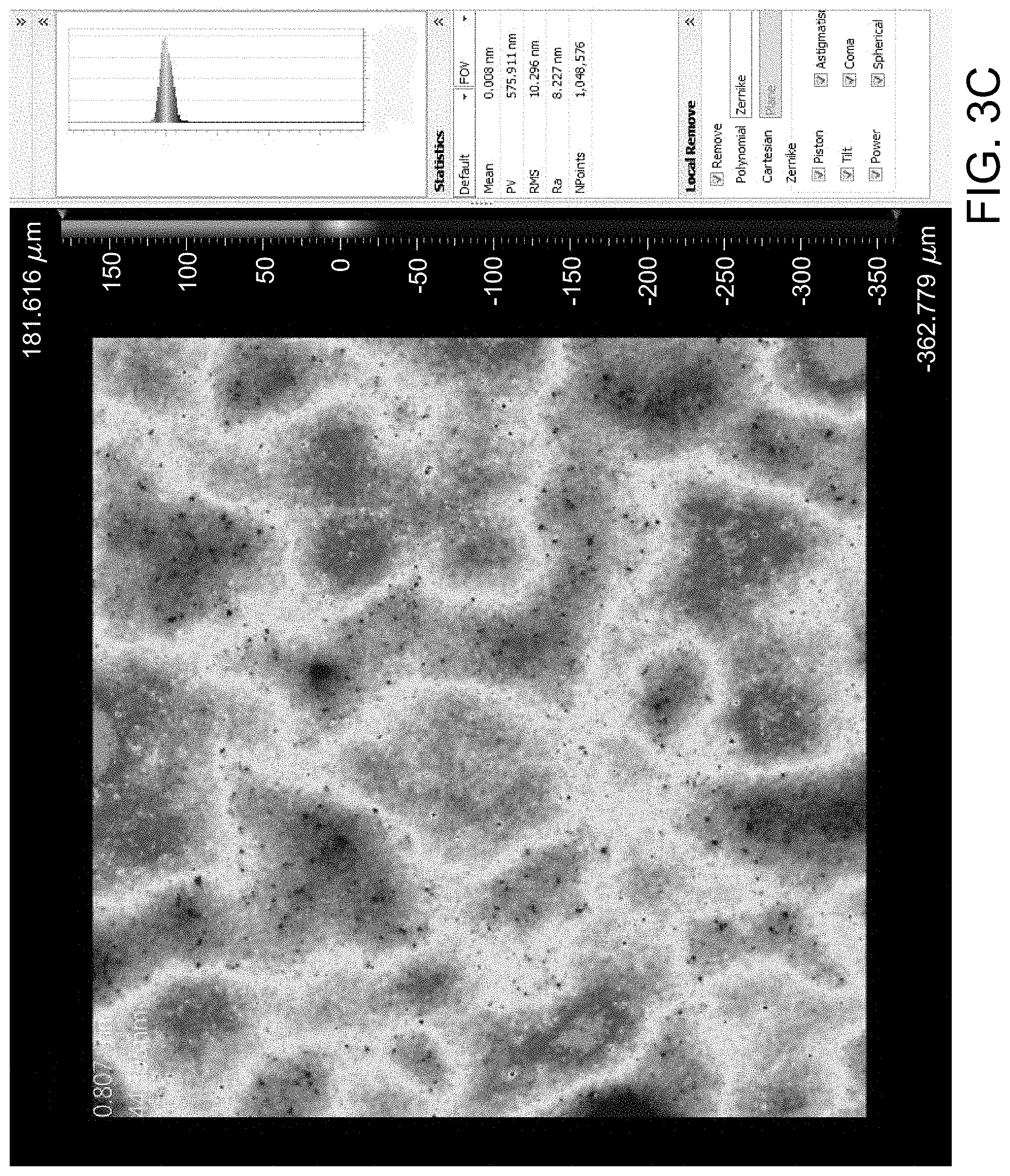
[0008] FIGS. 3A-3C illustrate surface maps of a small portion of the ceramic sample at various steps of the one or more disclosed methods.
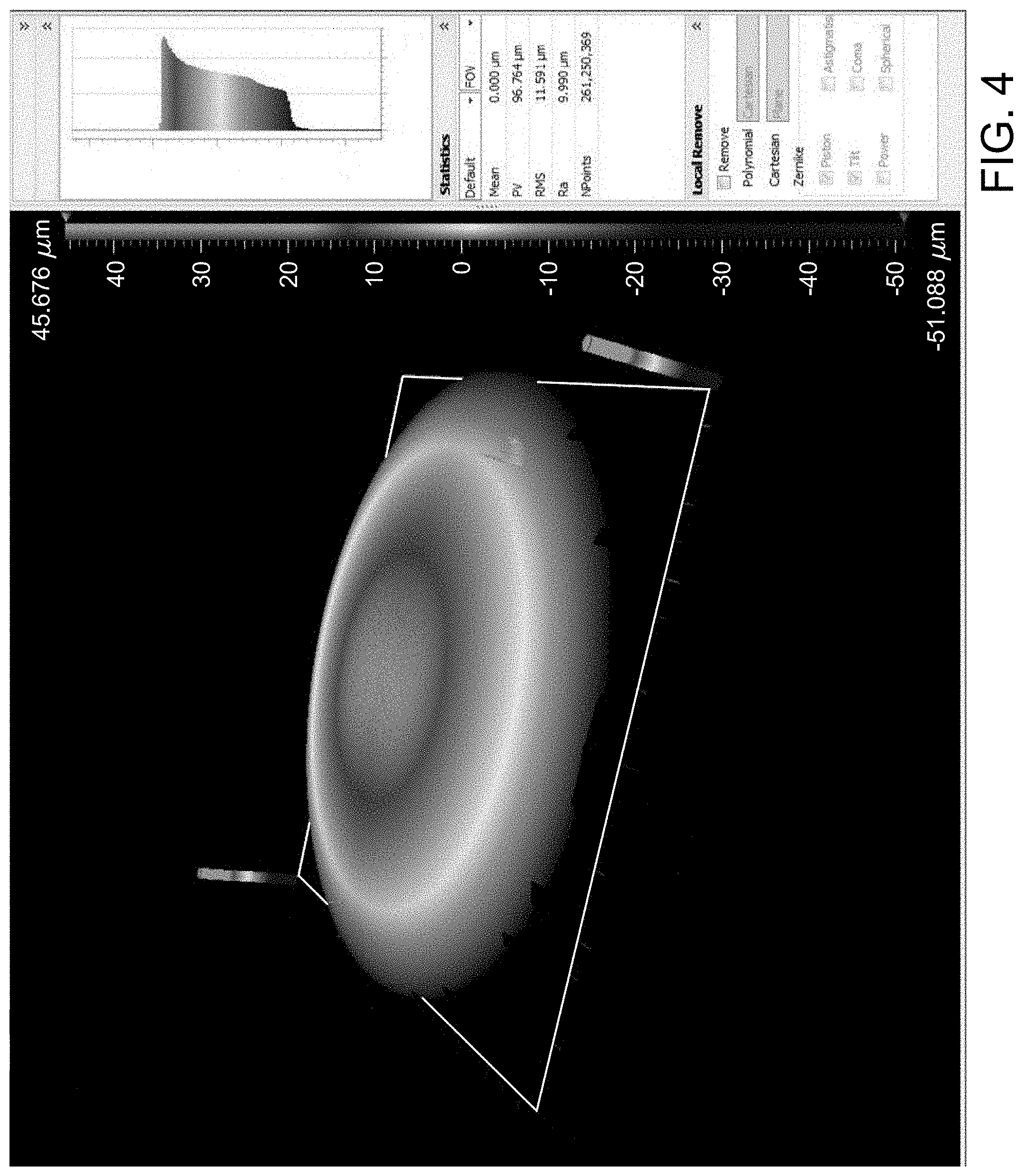
[0009] FIG. 4 illustrates an example 3-D full surface map after polishing in accordance with an aspect of the present disclosure.
[0010] FIG. 5 illustrates a polished ceramic sample.
DETAILED DESCRIPTION
[0011] The present disclosure describes systems and methods for polishing ceramic materials or components of adaptive optical systems, such as ceramics comprising zirconium diboride machined for optical grade applications (e.g., facesheets for a DM having a surface roughness error of 20 nm RMS or less). Systems and methods for polishing according to the present disclosure may provide one or more polished components to be integrated into an adaptive optical system. As a non-limiting example, and in accordance with aspects of the present disclosure, a ceramic material (e.g., zirconium diboride ceramics, ceramics comprising about 75% ZrB.sub.2 and about 25% SiC, etc.), may be used in the adaptive optics system. Such polished components, if comprised of the same material, may be utilized in the adaptive optical system to reduce or substantially eliminate thermally induced aberrations by preventing certain causes of thermal expansion.
[0012] FIG. 1 illustrates a process flow chart of a method 100 in accordance with the present disclosure. Prior to a first step of method 100, a sample (e.g., an optical component) may be manufactured in a sintering furnace. As an example, a sample disk (e.g., 3 inch diameter flat disk with 0.8 mm thickness) may be polished using the methods described herein. An initial shape of the sample (e.g., a flat disc) may be defined by coarse grinding. After sample fabrication, method 100 may move to a first step of measuring a sample thickness 110. Method 100 may reduce surface roughness through a plurality of polishing steps as disclosed herein to achieve an adaptive optical system component (e.g., a mirror) having surface deformations of less than about 2 nm RMS on spatial scales below about a millimeter.
[0013] If the sample has a thickness within an acceptable range for use in an adaptive optical system, method 100 may move to a step of fine grinding 120. Method 100 may include, for instance, fine grinding of the sample on a first machine. In some instances of the disclosure, first machine comprises a CNC machine. FIG. 2A illustrates a CNC machine that may be used in one or more of the disclosed methods. The CNC machine may be driven by a custom code written in Matlab. Multiple different parameters of the machine, such as the polishing compound, speed, and pressure may be adjusted to accomplish fine grinding to a target roughness. In exemplary embodiments, the surface roughness of a sample may be decreased from a starting roughness of about 0.265 .mu.m to and end roughness of about 0.1330 .mu.m RMS. A diamond disc system (e.g., a Trizact diamond disc system) may be utilized to accomplish a first fine grinding step. For instance, a 9 .mu.m Trizact disc and a slurry of Al.sub.2O.sub.3 and coolant may be utilized. In some embodiments, the slurry may be comprised of a slurry of 5 .mu.m Al.sub.2O.sub.3 and Sabre coolant. However, it is understood that other configurations and slurries may be used. In embodiments, diamond grit sizes of 20, 9, and 3 .mu.m at 2.552 PSI and a speed of 500 mm/min may be selected at various grinding and/or polishing steps of the method 100. If the sample is outside of an acceptable thickness range, method 100 may proceed to interim step 115 of grinding the sample, and the sample may then be remeasured (e.g., step 110) until a target thickness is achieved. Step 115 may be accomplished using one or more diamond discs (e.g., 90 .mu.m diamond discs).
[0014] Method 100 may then move to a step of measuring a surface roughness error (e.g., RMS) of the sample 130. As described herein, the surface roughness may be measured at one or more intervals during the method 100. In some instance, RMS may be measured using a Zygo white-light interferometer. However, other means of measuring the surface roughness may be used, as would be appreciated by one of skill in the art. If the RMS is around 185 nm, method may move to a second step of fine grinding 140. In some embodiments, a 3 .mu.m Trizact and a slurry of 5 .mu.m Al.sub.2O.sub.3 and coolant may be utilized. If the RMS is outside of the range of about 185 nm, then previous method steps may be repeated until the RMS is around 185 nm.
[0015] After the second fine grinding step 140, the RMS of the sample may be measured 150, and, if the RMS is about 135 nm or less, method 100 may move to a step of fine polishing the sample 160. Following the CNC machining, a Strasbaugh machine may be utilized for finer polishing. FIG. 2B illustrates a Strasbaugh machine that may be used in one or more of the disclosed methods. A Strasbaugh machine may provide faster polishing times but allows for easy deterioration of the shape of the material being polished. In some embodiments, a first step of fine polishing the sample 160 may be accomplished using a diamond powder and a slurry of olive oil and deionized water. For instance, a 1.5 .mu.m diamond powder may be mixed with olive oil and deionized water. This slurry may be applied, for instance, to a pellon pad to accomplish the fine polishing. In embodiments, successive particle sizes of 1.5 and 0.5 .mu.m may be utilized in this or other fine polishing steps. In embodiments, this step may lower the surface roughness to about 7 nm RMS.
[0016] After the first fine polishing step 160, the RMS of the sample may be measured 170, and, if the RMS is around 20 nm, method 100 may move to a second step of fine polishing the sample 180. Second fine polishing step 180 may be accomplished with 0.5 .mu.m diamond powder and a slurry of olive oil and deionized water.
[0017] After the second fine polishing step 180, the RMS of the sample may be measured 190, and, if the RMS is around 10 nm, method 100 may move to a third step of fine polishing 200. In some embodiments, third fine polishing step 200 may be accomplished with 0.1 .mu.m diamond powder and a slurry of olive oil and deionized water.
[0018] After the third fine polishing step 200, the RMS of the sample may be measured 210, and, if the RMS is around 2 nm, method 100 may conclude 220 and a resultant polished sample may be ready for use in an adaptive optical system. If the RMS is greater than around 2 nm, the third step of fine polishing 200 may be repeated until the sample reaches an RMS of around 2 nm.
[0019] Examples of the specifications for each of the grinding and polishing steps are listed below in Table 1.
TABLE-US-00001 Polishing Pressure Polishing Resulting Machine Compound (PSI) Speed Radius (mm) RMS (nm) CNC Trizact (20 .mu.m), 2.552 500 mm/min 3 328 Al.sub.2O.sub.3 (5 .mu.m), Sabre Coolant CNC Trizact (9 .mu.m), 2.552 500 mm/min 3 184 Al.sub.2O.sub.3 (5 .mu.m), Sabre Coolant CNC Trizact (3 .mu.m), 2.552 500 mm/min 3 133 Al.sub.2O.sub.3 (5 .mu.m), Sabre Coolant Strasbaugh Diamond (1.5 .mu.m), 2.552 Eccentric: 35 RPM 30 20 Olive Oil, Spindle: 50 RPM Deionized Water Strasbaugh Diamond (0.5 .mu.m), 2.552 Eccentric: 30 RPM 30 7 Olive Oil, Spindle: 50 RPM Deionized Water
However, it is understood that the decision points based on satisfying a particular surface roughness may be example thresholds and such process includes other thresholds within +/-20% of the enumerated thresholds. Other tolerances may be used without departing from the invention. It is further understood that throughout the polishing process, other forms of polishing compound, such as SiC and Al.sub.2O.sub.3, may be used.
[0020] FIGS. 3A-3C illustrate surface maps of a small portion of the ceramic sample, approximately 0.8 mm on a side generated at one or more key intervals in the polishing process. FIG. 3A shows a surface map at the beginning of the polishing process with the RMS surface error at about 265 nm. FIG. 3B shows a surface map following Trizact polishing, with the RMS surface error reduced to about 110 nm. FIG. 3C shows a surface map towards the end of polishing, with the surface quality at about 10 nm RMS.
[0021] In FIG. 4, a map of a whole sample surface is illustrated. The map is comprised of hundreds of successive measurements across the entirety of the sample taken using the white-light interferometer and stitched together to form the map. In the illustrated map, the sample (e.g., a ceramic component comprising zirconium diboride) has been polished to a low surface roughness (e.g., less than 40 nm, 30 nm, 20 nm, 10 nm, 2 nm RMS). Significant power is shown in the surface of the sample, caused by edge roll-down from the Strasbaugh machine. In embodiments of the disclosed method, the CNC machine may provide improved control of the shape of sample during one or more steps of the polishing method. To maintain the flat figure, controlled polishing can accomplished with the CNC machine. The finer control possible with the CNC machine may limit this error and the shape may be held to a higher standard.
[0022] FIG. 5 illustrates a polished ceramic sample. The polished sample may be, for instance, a ceramic disk having a diameter of about 30 mm and a thickness of about 6 mm. Once polished down to a surface roughness of between about 40 nm-2 nm RMS, including 40 nm, 30 nm, 20 nm, 10 nm, and 2 nm or less (and including intervening end points), the sample (e.g., mirror) may be optically and mechanically tested.
[0023] As described herein, methods for preparing a ceramic material may provide for the manufacture of aspheric ceramic facesheets for a DM that may be incorporated as the primary or secondary mirrors of adaptively corrected telescopes. It is understood that other components may be prepared using the same or similar methods. A facesheet according to embodiments of the disclosure may be lightweight and robust, with a thickness of about 0.8 mm, for example, and may be capable of handling high power density. In some embodiments, a ceramic comprising zirconium diboride may be utilized to polish to an optical finish (e.g., less than 40 nm, 30 nm, 20 nm, 10 nm, 2 nm RMS). The material may be durable having, for instance, a bulk modulus of about 5 times that of conventional glass. Thus, a complete optical system may be built that is robust and substantially lighter than a conventional glass and metal system.
[0024] As described herein, the ZrB.sub.2 materials are of interest for more than their athermal properties. They are also relatively light-weight, durable, and very strong. This allows for adaptation to many different optical systems.
* * * * *
D00000
D00001
D00002
D00003
D00004
D00005
D00006
D00007
D00008
XML
uspto.report is an independent third-party trademark research tool that is not affiliated, endorsed, or sponsored by the United States Patent and Trademark Office (USPTO) or any other governmental organization. The information provided by uspto.report is based on publicly available data at the time of writing and is intended for informational purposes only.
While we strive to provide accurate and up-to-date information, we do not guarantee the accuracy, completeness, reliability, or suitability of the information displayed on this site. The use of this site is at your own risk. Any reliance you place on such information is therefore strictly at your own risk.
All official trademark data, including owner information, should be verified by visiting the official USPTO website at www.uspto.gov. This site is not intended to replace professional legal advice and should not be used as a substitute for consulting with a legal professional who is knowledgeable about trademark law.