Thin-film Deposition Method And Manufacturing Method Of Semiconductor Device
Lee; ManSu ; et al.
U.S. patent application number 16/454063 was filed with the patent office on 2020-01-02 for thin-film deposition method and manufacturing method of semiconductor device. The applicant listed for this patent is ASM IP Holding B.V.. Invention is credited to SeungWoo Choi, SungKyu Kang, MinSoo Kim, EunSook Lee, ManSu Lee.
| Application Number | 20200002812 16/454063 |
| Document ID | / |
| Family ID | 69007947 |
| Filed Date | 2020-01-02 |


View All Diagrams
| United States Patent Application | 20200002812 |
| Kind Code | A1 |
| Lee; ManSu ; et al. | January 2, 2020 |
THIN-FILM DEPOSITION METHOD AND MANUFACTURING METHOD OF SEMICONDUCTOR DEVICE
Abstract
A method of depositing a thin film having a desired etching characteristic while improving a loss amount and loss uniformity of a lower film includes, on the semiconductor substrate and the pattern structure: a first operation of depositing a portion of the thin film by repeating a first cycle comprising (a1) a source gas supply operation, (b1) a reactant gas supply operation, and (c1) a plasma supply operation for a certain number of times; a second operation of depositing a remaining portion of the thin film by repeating a second cycle comprising (a2) a source gas supply operation, (b2) a reactant gas supply operation, and (c2) a plasma supply operation for a certain number of times after the first operation, wherein a supply time of the source gas supply operation (a1) is longer than a supply time of the source gas supply operation (a2).
| Inventors: | Lee; ManSu; (Osan-si, KR) ; Kang; SungKyu; (Hwaseong-si, KR) ; Lee; EunSook; (Ansan-si, KR) ; Kim; MinSoo; (Suwon-si, KR) ; Choi; SeungWoo; (Cheonan-si, KR) | ||||||||||
| Applicant: |
|
||||||||||
|---|---|---|---|---|---|---|---|---|---|---|---|
| Family ID: | 69007947 | ||||||||||
| Appl. No.: | 16/454063 | ||||||||||
| Filed: | June 27, 2019 |
| Current U.S. Class: | 1/1 |
| Current CPC Class: | C23C 16/045 20130101; H01L 21/0337 20130101; C23C 16/45536 20130101; C23C 16/45542 20130101; H01L 21/0332 20130101; H01L 21/02164 20130101; H01L 21/0234 20130101; H01L 21/31111 20130101; C23C 16/455 20130101; C23C 16/45527 20130101; H01L 21/02274 20130101; H01L 21/02219 20130101; C23C 16/45523 20130101; C23C 16/402 20130101; H01L 21/0228 20130101 |
| International Class: | C23C 16/455 20060101 C23C016/455; H01L 21/033 20060101 H01L021/033 |
Foreign Application Data
| Date | Code | Application Number |
|---|---|---|
| Jun 29, 2018 | KR | 10-2018-0076113 |
Claims
1. A method of depositing a thin film on a pattern structure of a semiconductor substrate, the method comprising, on the semiconductor substrate and the pattern structure: a first operation of depositing a portion of the thin film by repeating a first cycle comprising a source gas supply operation (a1), a reactant gas supply operation (b1), and a plasma supply operation (c1) for a certain number of times; and a second operation of depositing a remaining portion of the thin film by repeating a second cycle comprising a source gas supply operation (a2), a reactant gas supply operation (b2), and a plasma supply operation (c2) for a certain number of times after the first operation, wherein a supply time of the source gas supply operation (a1) is longer than a supply time of the source gas supply operation (a2).
2. The method of claim 1, wherein the supply time of the source gas supply operation (a1) is two to five times the supply time of the source gas supply operation (a2).
3. The method of claim 1, wherein the supply time of the source gas supply operation (a1) is 0.2 seconds to 1 second.
4. The method of claim 1, wherein the number of repetitions of the first cycle is less than the number of repetitions of the second cycle.
5. The method of claim 1, wherein a ratio of the number of repetitions of the first cycle to the number of repetitions of the second cycle is 1/12 to 1/10.
6. The method of claim 1, wherein a loss amount and loss uniformity of the pattern structure is adjusted by controlling at least one of the supply time of the source gas supply operation (a1), plasma power of the plasma supply operation (c1), and a plasma duty ratio of the plasma supply operation (c1) in the first operation.
7. The method of claim 6, wherein the loss amount of the pattern structure during the first operation is reduced when the supply time of the source gas supply operation (a1) is increased.
8. The method of claim 6, wherein the loss amount of the pattern structure during the first operation is reduced and the loss uniformity of the pattern structure is improved by increasing the plasma power of the plasma supply operation (c1) and decreasing the plasma duty ratio of the plasma supply operation (c1) while maintaining multiplication of the plasma power by the plasma duty ratio of the plasma supply operation (c1) constant.
9. The method of claim 8, wherein the plasma power of the plasma supply operation (c1) in the first operation is in the range of about 650 W to about 1200 W, and the plasma duty ratio of the plasma supply operation (c1) in the first operation is in the range of about 25% to about 50%.
10. The method of claim 1, wherein plasma power of the plasma supply operation (c1) is greater than plasma power of the plasma supply operation (c2), and a plasma duty ratio of the plasma supply operation (c1) is less than a plasma duty ratio of the plasma supply operation (c2).
11. The method of claim 1, wherein a desired wet etch rate (WER) of the thin film is obtained by controlling at least one of plasma power of the plasma supply operation (c2) and a plasma duty ratio of the plasma supply operation (c2).
12. The method of claim 11, wherein the WER of the thin film is reduced when the plasma power of the plasma supply operation (c2) is increased.
13. The method of claim 11, wherein the WER of the thin film is reduced when the plasma duty ratio of the plasma supply operation (c2) is increased.
14. A method of depositing a thin film on a pattern structure of a semiconductor substrate, the method comprising: repeating a first cycle of applying first plasma power in a pulse form m times while using a plasma atomic layer deposition process, and improving a loss amount and loss uniformity of the pattern structure; and repeating a second cycle of applying second plasma power in a pulse form n times while using the plasma atomic layer deposition process, and depositing the thin film.
15. The method of claim 14, wherein the improving of the loss amount and loss uniformity of the pattern structure comprises: improving the loss amount and loss uniformity of the pattern structure by increasing a supply time of a source gas supply operation in the plasma atomic layer deposition process.
16. The method of claim 14, wherein the improving of the loss amount and loss uniformity of the pattern structure comprises: improving the loss amount and loss uniformity of the pattern structure by adjusting at least one of the first plasma power and a duty ratio.
17. The method of claim 14, further comprising forming the thin film by setting a ratio of the number of repetitions (m times) of the first cycle to the number of repetitions (n times) of the second cycle to 1/12 to 1/10.
18. The method of claim 14, wherein the depositing of the thin film by repeating the second cycle n times comprises: controlling a wet etch rate (WER) of the thin film by adjusting at least one of the second plasma power and a duty ratio.
19. The method of claim 14, further comprising: removing at least a portion of the thin film to form a spacer pattern of the thin film, wherein the spacer pattern of the thin film has a constant linewidth size over the semiconductor substrate.
20. A method of depositing a thin film on a pattern structure of a semiconductor substrate, the method comprising: improving a loss amount and loss uniformity of the pattern structure by controlling at least one of a supply time of a source gas supply operation, plasma power and a plasma duty ratio of a plasma supply operation while using a plasma atomic layer deposition process; and controlling a wet etch rate (WER) of the thin film by controlling at least one of the plasma power and the plasma duty ratio of the plasma supply operation while using the plasma atomic layer deposition process.
Description
CROSS-REFERENCE TO RELATED APPLICATION
[0001] This application claims the benefit of Korean Patent Application No. 10-2018-0076113, filed on Jun. 29, 2018, in the Korean Intellectual Property Office, the disclosure of which is incorporated herein in its entirety by reference.
BACKGROUND
1. Field
[0002] One or more embodiments relate to a thin-film deposition method and a manufacturing method of a semiconductor device, and more particularly, to a method of depositing a thin-film by a plasma atomic layer deposition method on a pattern structure of a substrate and a method of manufacturing a semiconductor device.
2. Description of the Related Art
[0003] Due to the diversification of patterning technology of DRAM products, it is required to precisely control a spin on hardmask (SOH), which is a material used as a photoresist (PR) or hard mask in a double patterning technology (DPT) process.
[0004] In general, when a thin film is deposited on an SOH film using a plasma process, SOH loss occurs in the SOH film due to plasma radicals. In some cases, the degree of loss varies depending on each portion of a substrate. Due to the non-uniformity of the loss, critical dimension (CD) spacing becomes irregular when fine patterning is performed, thereby lowering the yield of a product, resulting in productivity and economic loss.
[0005] Technological development is required to improve not only the total loss of SOH but also SOH loss uniformity. Since the quality of a thin film formed on an SOH thin-film needs to be considered, technology to control quality is needed.
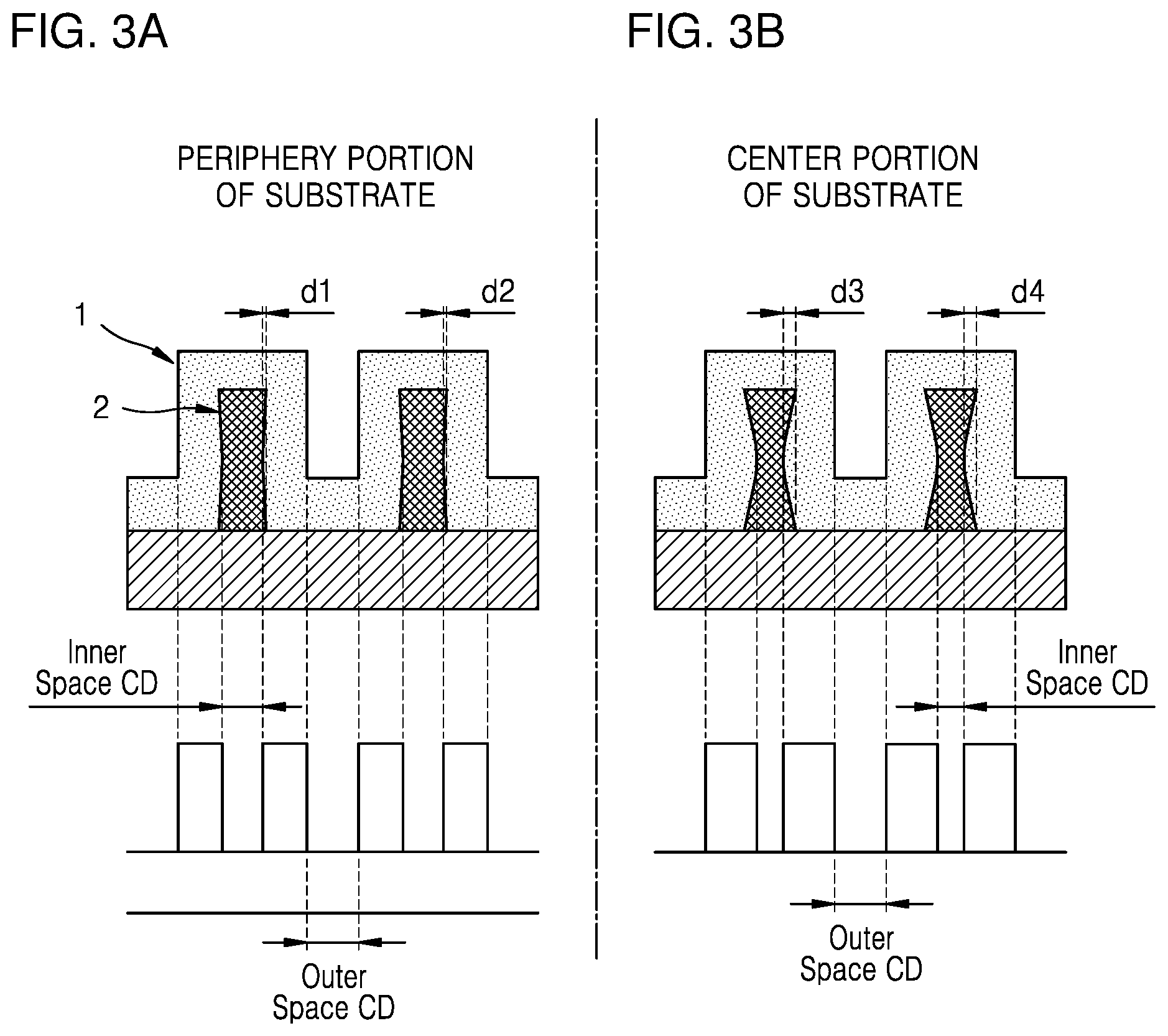
SUMMARY
[0006] One or more embodiments include a method of depositing a thin film having desired etching characteristics while adjusting a loss amount and loss uniformity of a lower film to a desired level during thin-film deposition.
[0007] One or more embodiments include a method of improving the loss amount and loss uniformity of a pattern when depositing a thin film on a pattern of a semiconductor substrate and at the same time controlling a wet etch rate (WER) of the thin film formed on the semiconductor pattern.
[0008] One or more embodiments include a method of manufacturing a semiconductor device capable of improving the loss uniformity of a pattern when depositing a thin film on a pattern of a semiconductor substrate and forming a more uniform spacer mask over the entire substrate.
[0009] Additional aspects will be set forth in part in the description which follows and, in part, will be apparent from the description, or may be learned by practice of the presented embodiments.
[0010] According to one or more embodiments, a method of depositing a thin film is performed on a pattern structure of a semiconductor substrate, and includes, on the semiconductor substrate and the pattern structure: a first operation of depositing a portion of the thin film by repeating a first cycle including a source gas supply operation (a1), a reactant gas supply operation (b1), and a plasma supply operation (c1) for a certain number of times; and a second operation of depositing a remaining portion of the thin film by repeating a second cycle including a source gas supply operation (a2), a reactant gas supply operation (b2), and a plasma supply operation (c2) for a certain number of times after the first operation, wherein a supply time of the source gas supply operation (a1) is longer than a supply time of the source gas supply operation (a2).
[0011] The supply time of the source gas supply operation (a1) may be two to five times the supply time of the source gas supply operation (a2).
[0012] The supply time of the source gas supply operation (a1) may be 0.2 seconds to 1 second.
[0013] The number of repetitions of the first cycle may be less than the number of repetitions of the second cycle.
[0014] A ratio of the number of repetitions of the first cycle to the number of repetitions of the second cycle may be 1/12 to 1/10.
[0015] A loss amount and loss uniformity of the pattern structure may be adjusted by controlling at least one of the supply time of the source gas supply operation (a1), plasma power of the plasma supply operation (c1), and a plasma duty ratio of the plasma supply operation (c1) in the first operation. The loss amount of the pattern structure during the first operation may be reduced when the supply time of the source gas supply operation (a1) is increased. The loss amount of the pattern structure during the first operation may be reduced and the loss uniformity of the pattern structure may be improved by increasing the plasma power of the plasma supply operation (c1) and decreasing the plasma duty ratio of the plasma supply operation (c1) while maintaining multiplication of the plasma power by the plasma duty ratio of the plasma supply operation (c1), which is the plasma power amount, constant. The plasma power of the plasma supply operation (c1) in the first operation may be in the range of about 650 W to about 1200 W, and the plasma duty ratio of the plasma supply operation (c1) in the first operation may be in the range of about 25% to about 50%.
[0016] Plasma power of the plasma supply operation (c1) may be greater than plasma power of the plasma supply operation (c2), and a plasma duty ratio of the plasma supply operation (c1) may be less than a plasma duty ratio of the plasma supply operation (c2).
[0017] A desired wet etch rate (WER) of the thin film may be obtained by controlling at least one of plasma power of the plasma supply operation (c2) and a plasma duty ratio of the plasma supply operation (c2). The WER of the thin film may be reduced when the plasma power of the plasma supply operation (c2) is increased. The WER of the thin film may be reduced when the plasma duty ratio of the plasma supply operation (c2) is increased.
[0018] According to one or more embodiments, a method of depositing a thin film on a pattern structure of a semiconductor substrate includes: repeating a first cycle of applying first plasma power in a pulse form m times while using a plasma atomic layer deposition process, and improving a loss amount and loss uniformity of the pattern structure; and repeating a second cycle of applying second plasma power in a pulse form n times while using the plasma atomic layer deposition process, and depositing the thin film.
[0019] The improving of the loss amount and loss uniformity of the pattern structure may include: improving the loss amount and loss uniformity of the pattern structure by increasing a supply time of a source gas supply operation in the plasma atomic layer deposition process.
[0020] The improving of the loss amount and loss uniformity of the pattern structure may include: improving the loss amount and loss uniformity of the pattern structure by adjusting at least one of the first plasma power and a duty ratio.
[0021] The method of depositing the thin film may further include: forming the thin film by setting a ratio of the number of repetitions (m times) of the first cycle to the number of repetitions (n times) of the second cycle to 1/12 to 1/10.
[0022] The depositing of the thin film by repeating the second cycle n times may include: controlling a wet etch rate (WER) of the thin film by adjusting at least one of the second plasma power and a duty ratio.
[0023] The method of depositing a thin film may further include: removing at least a portion of the thin film to form a spacer pattern of the thin film, wherein the spacer pattern of the thin film has a constant linewidth size over the substrate.
[0024] According to one or more embodiments, a method of depositing a thin film on a pattern structure of a semiconductor substrate includes: improving a loss amount and loss uniformity of the pattern structure by controlling at least one of a supply time of a source gas supply operation, plasma power and a plasma duty ratio of a plasma supply operation while using a plasma atomic layer deposition process; and controlling a wet etch rate (WER) of the thin film by controlling at least one of the plasma power and the plasma duty ratio of the plasma supply operation while using the plasma atomic layer deposition process.
BRIEF DESCRIPTION OF THE DRAWINGS
[0025] These and/or other aspects will become apparent and more readily appreciated from the following description of the embodiments, taken in conjunction with the accompanying drawings in which:
[0026] FIGS. 1 and 2 are timing diagrams of a thin-film deposition method according to embodiments of the inventive concept;
[0027] FIGS. 3A and 3B illustrate problems occurring during thin-film deposition using the conventional processes of FIGS. 1 and 2;
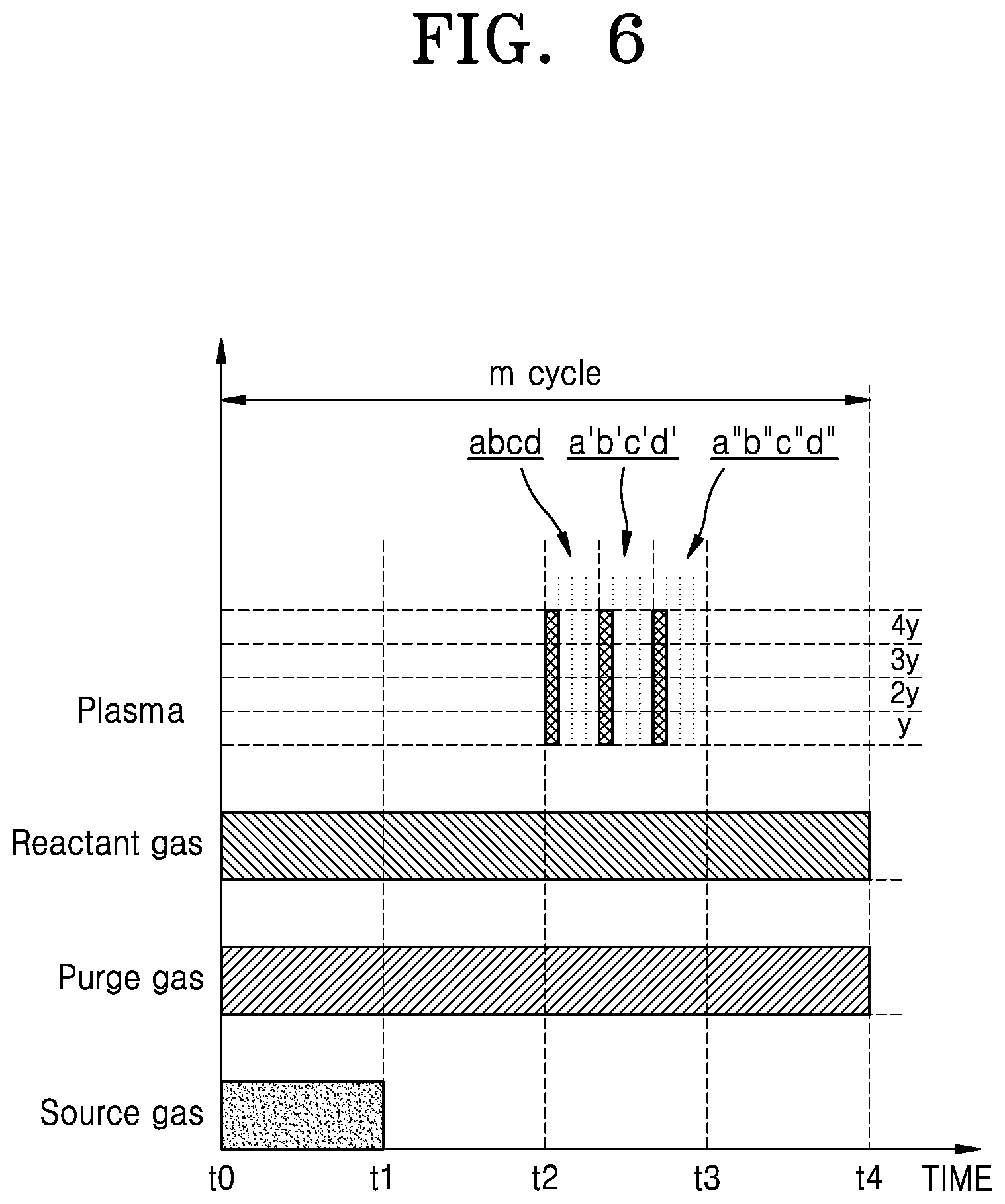
[0028] FIGS. 4 to 6 are timing diagrams illustrating a thin-film deposition method according to other embodiments of the inventive concept;
[0029] FIGS. 7 and 8 are graphs illustrating a wet etch rate (WER) characteristic of a film and damage to a lower film according to a duty ratio when plasma is supplied onto a substrate in a continuous mode and a pulse mode;
[0030] FIG. 9 is a timing diagram illustrating a thin-film deposition method according to other embodiments of the inventive concept;
[0031] FIG. 10 is a table of an example of process parameters that can be used in a thin-film deposition method according to the other embodiments of the inventive concept;
[0032] FIG. 11 is a graph illustrating a spin on hardmask (SOH) loss amount depending on a substrate position, which is generated when plasma is supplied onto a substrate in a continuous mode and a pulse mode in a first operation;
[0033] FIG. 12 is a table of SOH loss uniformity and a WER of a thin film according to a source supply time in a first operation;
[0034] FIG. 13 is a table comparing an SOH loss amount and SOH loss uniformity in a case where the first operation is performed and in a case where the first operation is not performed; and
[0035] FIGS. 14 to 18 are cross-sectional views illustrating a method of manufacturing a semiconductor device according to the other embodiments of the inventive concept.
DETAILED DESCRIPTION
[0036] Hereinafter, one or more embodiments will be described more fully with reference to the accompanying drawings.
[0037] In this regard, the present embodiments may have different forms and should not be construed as being limited to the descriptions set forth herein. Rather, these embodiments are provided so that the present disclosure will be thorough and complete, and will fully convey the scope of the present disclosure to one of ordinary skill in the art.
[0038] The terminology used herein is for the purpose of describing particular embodiments and is not intended to limit the present disclosure. As used herein, the singular forms "a", "an", and "the" are intended to include the plural forms as well, unless the context clearly indicates otherwise. It will be further understood that the terms "includes", "comprises" and/or "including", "comprising" used herein specify the presence of stated features, integers, steps, operations, members, components, and/or groups thereof, but do not preclude the presence or addition of one or more other features, integers, steps, operations, members, components, and/or groups thereof. As used herein, the term "and/or" includes any and all combinations of one or more of the associated listed items. Expressions such as "at least one of," when preceding a list of elements, modify the entire list of elements and do not modify the individual elements of the list
[0039] It will be understood that, although the terms first, second, etc. may be used herein to describe various members, components, regions, layers, and/or sections, these members, components, regions, layers, and/or sections should not be limited by these terms. These terms do not denote any order, quantity, or importance, but rather are only used to distinguish one component, region, layer, and/or section from another component, region, layer, and/or section. Thus, a first member, component, region, layer, or section discussed below could be termed a second member, component, region, layer, or section without departing from the teachings of embodiments.
[0040] Hereinafter, embodiments of the present disclosure will be described with reference to the accompanying drawings. In the drawings, variations from the illustrated shapes may be expected as a result of, for example, manufacturing techniques and/or tolerances. Thus, the embodiments of the present disclosure should not be construed as being limited to the particular shapes of regions illustrated herein but may include deviations in shapes that result, for example, from manufacturing processes.
[0041] FIG. 1 is a timing diagram illustrating a thin-film deposition method according to embodiments of the inventive concept.
[0042] Referring to FIG. 1, the thin-film deposition method includes a source gas supply operation, a reactant gas supply operation, and a plasma supply operation.
[0043] In the source gas supply operation, a source gas is chemisorbed onto a substrate while being supplied to a reaction space for a time t0 to t1.
[0044] Thereafter, the supply of the source gas is stopped for a time t1 to t2, and a purge gas is supplied to a reaction space to discharge the source gas remaining in the reaction space to the outside of a reactor.
[0045] In the reactant gas supply operation and the plasma supply operation, a thin-film layer is formed while a reactant gas is supplied to the reaction space for a time t2 to t3 and chemically reacts with the chemisorbed source gas on the substrate. Plasma is supplied for the time t2 to t3 such that the thin film layer may be formed at a low temperature (i.e., a chemical reaction may occur at a low temperature), so that the reactant gas is ionized to chemically react with the source gas to form the thin film layer. Thereafter, the supply of the reactant gas is stopped for a time t3 to t4, and the remaining reactant gas is removed from the reactor while the purge gas is supplied again.
[0046] One process for forming such a unit thin film is defined as a cycle. That is, the time t0 to t4 shown in FIG. 1 is defined as one cycle, and a thin film having a desired thickness may be formed while repeating the cycle several times.
[0047] FIG. 2 is a timing diagram illustrating a thin-film deposition method according to embodiments of the inventive concept. The thin-film deposition method according to these embodiments may be variations of the thin-film deposition method according to the embodiments shown in FIG. 1. Hereinafter, repeated descriptions of the embodiments will not be given herein.
[0048] Referring to FIG. 2, the thin-film deposition method may be performed in a plasma atomic layer deposition (PEALD) mode. For example, one cycle may be sequentially performed in the order of source gas supply (t0 to t1), purge (t1 to t2), reactant gas supply and plasma application (t2 to t3), and purge (t3 to t4).
[0049] In an alternative embodiment, a reactant gas and a purge gas may be continuously supplied to a reactor during the entire cycle. The reactant gas acts to purge the reactor together with the purge gas without reacting with a source gas when not activated by plasma. However, the reactant gas, when activated by the plasma, may be activated to chemically react with the source gas adsorbed on a substrate to form a thin film. That is, the reactant gas may act as a reactive purge gas.
[0050] FIG. 2 shows that the reactant gas is continuously supplied during the entire PEALD process cycle. However, in other embodiments, the reactant gas may be supplied only when the plasma is supplied, or may start to be supplied just before the plasma is supplied and may be stopped to be supplied when the plasma supply is stopped.
[0051] In other embodiments, when the reactant gas reacts with the source gas through a thermal reaction with the substrate, the reactant gas may be supplied only when the plasma is supplied and thus a thin film may be formed.
[0052] In the embodiments of FIG. 2, the plasma may be an in-situ plasma generated on the substrate or a remote plasma formed outside the reactor and directed into a reaction space. In other embodiments, the plasma may be another source (e.g., UV) that may activate the reactant gas.
[0053] According to embodiments of the inventive concept, the reactant gas chemically reacts with the source gas only when activated by the plasma and acts as the purge gas when not activated by the plasma, thereby acting as a reactive purge gas. Thus, the reactant gas may be continuously supplied from t0 to t4 in FIG. 2.
[0054] In other embodiments, if the reactant gas chemically reacts with the source gas even when the reactant gas is not activated by the plasma, the reactant gas may be supplied only for the time t2 to t3 during which the plasma is supplied (see FIG. 1).
[0055] According to embodiments of the inventive concept, a frequency of the plasma may be 27 MHz to 100 MHz during the plasma supply operation (t2 to t3). It is not desirable to apply a frequency of 100 MHz or more, because it is difficult to discharge the plasma in the reactor when plasma with the frequency of 100 MHz or more is applied. Thus, the frequency of the plasma may preferably be 60 MHz to 70 MHz.
[0056] A basic cycle is repeated until a thin film of a desired thickness is deposited with a basic cycle from t0 to t4, which is the time shown in FIG. 2.
[0057] According to the inventive concept, the source gas supply operation to the plasma supply operation are performed on a pattern structure (e.g., a structure with the height greater than the width) of a semiconductor substrate and are performed at a high frequency of 60 MHz or more during the plasma supply operation. The pattern structure may have an upper surface, a lower surface, and a side surface connecting the upper surface to the lower surface, wherein a length of the side surface may be greater than a width of the upper surface and may also be greater than a width of the lower surface.
[0058] The pattern structure may be a mask pattern in particular and may be formed of a material reactive with at least one of materials (e.g., the source gas and/or reactant gas) used during the thin-film deposition process described above, i.e., an atomic layer deposition process using plasma. The mask pattern may include, for example, a spin on hardmask (SOH) membrane or a carbon SOH (C--SOH) membrane.
[0059] For example, when the mask pattern is formed of an SOH and a silicon oxide layer (SiO.sub.2) is formed on the mask pattern using the thin-film deposition process, an oxygen gas may be supplied as a reactant gas. For example, an oxygen source as a reactant gas may include at least one of O.sub.3, N.sub.2O, and CO.sub.2 in addition to O.sub.2. In this case, since the oxygen gas is supplied during the plasma supply operation, damage (e.g., ashing) to the mask pattern may occur at the beginning of the process by oxygen plasma.
[0060] FIG. 3 shows a case where damage to a mask pattern occurs due to a radical when a thin film is deposited on the mask pattern by a PEALD mode. As described above, when an oxygen gas is used as a reactant gas during plasma supply, an oxygen radical may be generated. The oxygen radical reacts with materials of a hard mask pattern of an SOH membrane or a C--SOH membrane such that at least a portion (in particular, a portion of a sidewall) of a hard mask pattern structure may be removed during the plasma supply operation.
[0061] When the hard mask pattern structure is damaged during the plasma supply operation, a critical dimension (CD) difference between an inner space and an outer space of the hard mask pattern may occur.
[0062] In more detail, referring to a hard mask pattern of FIG. 3A, for example, in a case of a hard mask pattern located on the periphery portion of a substrate, a mask may not be substantially damaged even if plasma is supplied. As a result, an inner space CD and an outer space CD may be identical.
[0063] Meanwhile, referring to a hard mask pattern of FIG. 3B, for example, in a case of a hard mask pattern located on the center portion of a substrate, when plasma is supplied and oxygen is supplied as a reactant gas, a side wall of the hard mask pattern may be damaged due to the oxygen plasma. As a result, the inner space CD and the outer space CD become different from each other.
[0064] The difference between the inner space CD and the outer space CD affects a subsequent process using a double patterning technology (DPT) as follows. In the DPT process, a process of depositing an oxide film on a hard mask on a patterned substrate may be performed (see FIGS. 14 to 18). The hard mask is damaged during the oxide film deposition process, and the degree of damage may be different at the center and the periphery portion of the substrate. Therefore, when a subsequent wet etching operation is performed on the oxide film, the thickness of a residual oxide film at the center portion of the substrate and the thickness of a residual oxide film at the periphery portion of the substrate may be different from each other. Since such a residual oxide film acts as a mask of the subsequent DPT process, the non-uniformity of the thicknesses of the residual oxide films causes a problem of CD non-uniformity, which may cause a defective device.
[0065] That is, the difference between the internal space CD and the external space CD of the hard mask pattern causes misalignment of features generated thereby, which adversely affects the characteristics of the entire product.
[0066] Furthermore, referring to FIG. 3, it can be seen that the amounts of loss of hard mask patterns at the periphery (see FIG. 3A) of the substrate and the center (see FIG. 3B) of the substrate are different from each other. For example, an SOH loss amount d1 or d2 at the periphery portion of the substrate is different from an SOH loss amount d3 or d4 at the center portion of the substrate.
[0067] In this case, it becomes difficult to uniformly treat the entire surface of the substrate in the subsequent process. For example, in a process of compensating for the loss of the hard mask pattern through the subsequent process, it becomes difficult to perform uniform treatment over the entire surface of the substrate, and the failure rate of a device is increased.
[0068] In a substrate processing process of depositing and etching a thin film on the substrate, it is very important to keep the uniformity of each portion of the substrate constant in order to increase the yield of a semiconductor device. However, when the degree of damage is different for each part of the substrate, yield management of the device is greatly influenced.
[0069] Therefore, it is an important technical object to improve the loss uniformity of a hard mask (e.g., SOH) according to the position on the substrate while reducing the amount of loss of the hard mask and uniformly compensate for the loss of the hard mask across the entire substrate in the subsequent process.
[0070] The present disclosure proposes a method of forming a thin film (e.g., SiO.sub.2) having desired etching characteristics (e.g., WER) while minimizing the loss non-uniformity of the hard mask (e.g., SOH) according to the above-described position on the substrate.
[0071] According to an embodiment of the inventive concept, a thin-film deposition method includes an operation of improving the loss amount and loss uniformity of a hard mask pattern structure (first operation) and an operation of controlling a wet etching characteristic of a thin film (second operation). In the first operation, although high-frequency plasma is supplied in a pulse mode, power greater than power supplied in a continuous mode is applied in a relatively short time, thereby preventing the hard mask from being damaged which is originated from a radical (e.g., oxygen radical) applied for a long time. In addition, in the first operation, the function of a protective film against the hard mask pattern structure may be enhanced by sufficiently supplying a source gas before supplying the plasma. In the second operation, the wet etching characteristic of the thin film may be controlled by controlling at least one of plasma power and a plasma duty ratio in the plasma supply operation.
[0072] FIGS. 4 to 6 are timing diagrams illustrating a thin-film deposition method according to other embodiments of the inventive concept. The thin-film deposition method according to these embodiments may be variations of the thin-film deposition method according to the above-described embodiments. Hereinafter, repeated descriptions of the embodiments will not be given herein.
[0073] FIG. 4 shows a plasma supply operation in a continuous mode in which plasma is continuously supplied for the time t2 to t3, as in the embodiments of FIG. 2. During the plasma supply operation in the continuous mode, a certain amount of power may be applied.
[0074] In general, a unit of the amount of power is watt-hour (Wh), but a unit of the amount of power defined in the present specification is defined as watt-second (Ws). For example, in an embodiment, 400 W of power may be applied for 0.5 seconds, and the amount of power at that time may be 200 Ws.
[0075] FIGS. 5 and 6 show a plasma supply operation in a pulse mode in which plasma is intermittently supplied for the time t2 to t3. In the present embodiments, the plasma is intermittently supplied over a plurality of sub periods, and the plasma may be applied with a duty ratio of less than 100% (e.g., a duty ratio of 50% or less) during each sub period. Here, the duty ratio refers to a time for which the pulse is applied over the entire time for plasma generation step (in this case, t2 to t3).
[0076] Referring to FIGS. 5 and 6, the sub period may be repeated during a period t2 to t3. In FIG. 5, the sub period is repeated three times with the period t2 to t3 being abcd, a'b'c'd', and a''b''c''d'', and a total of twelve individual periods are formed. However, the number of repetitions is not limited thereto. Furthermore, in FIG. 5, widths of respective sub periods and/or individual periods are the same, but in another embodiment, the widths of respective sub periods and/or individual periods may be different from each other.
[0077] In the continuous mode of FIG. 4, the plasma is continuously supplied over the entire sub period of the period t2 to t3, while in the pulse mode of FIG. 5, the plasma is supplied to an individual period ab, a'b', a''b'' of the sub periods abcd, a'b'c'd', and a''b''c''d'' of the period t2 to t3 in a pulse form. Since the plasma is supplied over 50% of the area of each sub period, the duty ratio in FIG. 5 is 50%. Also, in order to make the amount of power of the plasma supplied to the periods of abcd, a'b'c'd', and a''b''c''d'' of FIG. 5 equal to the amount of power of the plasma supplied to the corresponding periods of FIG. 4, the magnitude of plasma power in a plasma pulse period in FIG. 5 is set to 2y, which is twice the magnitude y of plasma power in FIG. 4. For example, when plasma of 400 W is supplied in the continuous mode of FIG. 4, plasma of 800 W is supplied in the pulse mode of FIG. 5.
[0078] Similarly, in the continuous mode of FIG. 4, the plasma is continuously supplied over the entire sub period of the period t2 to t3, while in the pulse mode of FIG. 6, the plasma is supplied to an individual period a, a', a'' of the sub periods abcd, a'b'c'd', and a''b''c''d'' of the period t2 to t3 in a pulse form. Since the plasma is supplied over 25% of the area of each sub period, the duty ratio in FIG. 6 is 25%. Also, in order to make the amount of power of the plasma supplied to the periods of abcd, a'b'c'd', and a''b''c''d'' of FIG. 6 equal to the amount of power of the plasma supplied to the corresponding periods of FIG. 4, the magnitude of plasma power in a plasma pulse period in FIG. 6 is set to 4y, which is four times the magnitude y of the plasma power in FIG. 4. For example, when plasma of 400 W is supplied in the continuous mode of FIG. 4, plasma of 1600W is supplied in the pulse mode of FIG. 6.
[0079] For example, during the plasma supply operation, power of 120 Wt may be supplied at a frequency of 60 MHz. In this case, in the continuous mode, plasma of 400 W power may be supplied for about 0.3 seconds (see FIG. 4). In another embodiment, in a pulse mode having three sub periods and a duty ratio of 50%, plasma of 800 W power may be supplied over the three sub periods, wherein each sub period has a period of 0.1 seconds, and the plasma of 800 W power may be supplied for 0.05 second during one sub period (see FIG. 5). In another embodiment, in a pulse mode having three sub periods and a duty ratio of 25%, plasma of 1600 W power may be supplied over the three sub periods, wherein each sub period has a period of 0.1 seconds, and the plasma of 1600 W power may be supplied for 0.025 seconds during one sub period (see FIG. 6).
[0080] In the above-described embodiments, the sub period is divided into three parts but is not limited thereto. The sub period may be divided into two parts, four parts or more, and the magnitude of plasma power supplied to each area may be adjusted according to a set duty ratio.
[0081] Further, the values associated with the plasma power described in the above embodiments are exemplary only. Thus, for example, in a continuous mode, plasma is supplied onto a substrate with a duty ratio of 100%, and the magnitude of plasma power may range from 100 W to 1000 W. Meanwhile, in a pulse mode, the plasma is supplied onto the substrate at a duty ratio of 50%, and the magnitude of the plasma power may be in the range of twice the magnitude in the continuous mode, i.e., 200 W to 2000 W. In other embodiments, in a different pulse mode, the plasma is supplied onto the substrate at a duty ratio of 25%, and the magnitude of the plasma power may be in the range of four times the magnitude in the continuous mode, i.e., 400 W to 4000 W.
[0082] As described above, according to the embodiments of the inventive concept, plasma is applied in a pulse mode in which plasma power is intermittently supplied. That is, by supplying the plasma in the pulse mode but increasing the magnitude of the plasma, plasma power having the same amount of power as that supplied in the continuous mode may be supplied. By applying the pulse mode, damage to a lower film due to ion bombardment may be reduced.
[0083] FIGS. 7 and 8 show a wet etch rate (WER) characteristic of a thin film and the damage to a lower film according to a duty ratio and plasma power when plasma is supplied onto a substrate in a continuous mode and a pulse mode according to the above-described embodiments.
[0084] Referring to FIG. 7, when the duty ratio is 25%, 50% and 100%, respective WER characteristics of SiO.sub.2 deposited on a hard mask pattern are compared with each other. Here, the duty ratio 100% corresponds to the continuous mode. That is, FIG. 7 shows a comparison between the continuous mode (duty ratio 100%) and the pulse mode (duty ratios 25% and 50%).
[0085] In order to realize the same WER characteristic, the lower the duty ratio, the greater the plasma power supplied. For example, referring to a dashed line portion in FIG. 7, in order to achieve a WER of about 17 nm/min, plasma of about 400 W power is supplied in the continuous mode having a duty ratio of 100%, plasma of about 800 W power is supplied in the pulse mode having a duty ratio of 50%, and plasma of about 1600 W power is supplied in the pulse mode having a duty ratio of 25%. Referring to FIG. 7, it can be seen that the amounts of plasma power (a multiplier value of the plasma power and the duty ratio) supplied in respective cases are all the same.
[0086] Furthermore, from FIG. 7, it can be seen that a WER of a thin film (in this case, SiO.sub.2) may be controlled by controlling at least one of the plasma power and the plasma duty ratio of the plasma supply operation of FIG. 2. In more detail, it can be seen that the WER of the thin film may be reduced as the plasma power is increased while maintaining the plasma duty ratio constant, and the WER of the thin film may also be reduced as the plasma duty ratio is increased while maintaining the plasma power constant.
[0087] In view of the technical effect of the present disclosure, a desired WER of the thin film may be obtained by controlling at least one of the plasma power and the plasma duty ratio during thin-film deposition. This will be further described with reference to FIGS. 9 and 12.
[0088] FIG. 8 shows that the lower the duty ratio, the less the damage to the lower film. Referring to FIG. 8, when the lower film is formed of a hard mask of SOH, a lower film pattern may be deformed by an oxygen radical to be damaged when SiO.sub.2 is deposited on the hard mask by a PEALD mode, and it can be seen that the degree of damage depends on the manner of supplying plasma.
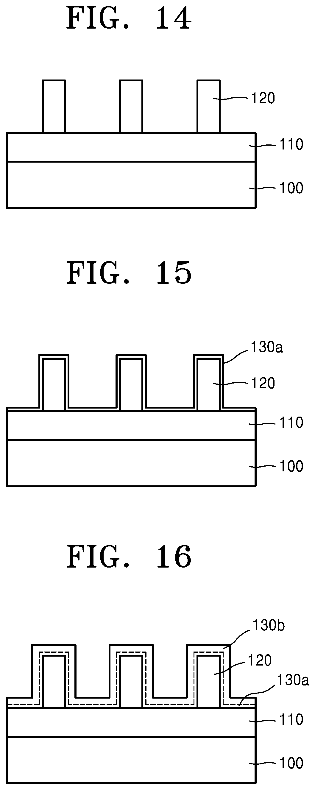
[0089] For example, as shown in the dashed line in FIG. 8, the degree of damage to the lower film pattern is about 65 angstroms when 400 W of power is supplied in a continuous mode, while the degree of damage to the lower film pattern is reduced to about 50 angstroms when 800 W of power is supplied in a pulse mode having a duty ratio of 50%, and the degree of damage to the lower film pattern is reduced to about 35 angstroms when 1600 W of power is supplied in a pulse mode having a duty ratio of 25%.
[0090] Therefore, considering FIGS. 7 and 8, it can be seen that the amount of loss of a lower film may be reduced when plasma (having substantially the same amount of power) is supplied in a pulse mode rather than in a continuous mode.
[0091] In the present invention, in view of such a technical effect, high frequency plasma is intermittently supplied in a pulse mode in performing a thin-film deposition process. This is because the damage to a lower mask may be minimized by supplying the plasma intermittently. This will be further described with reference to FIGS. 9 to 11.
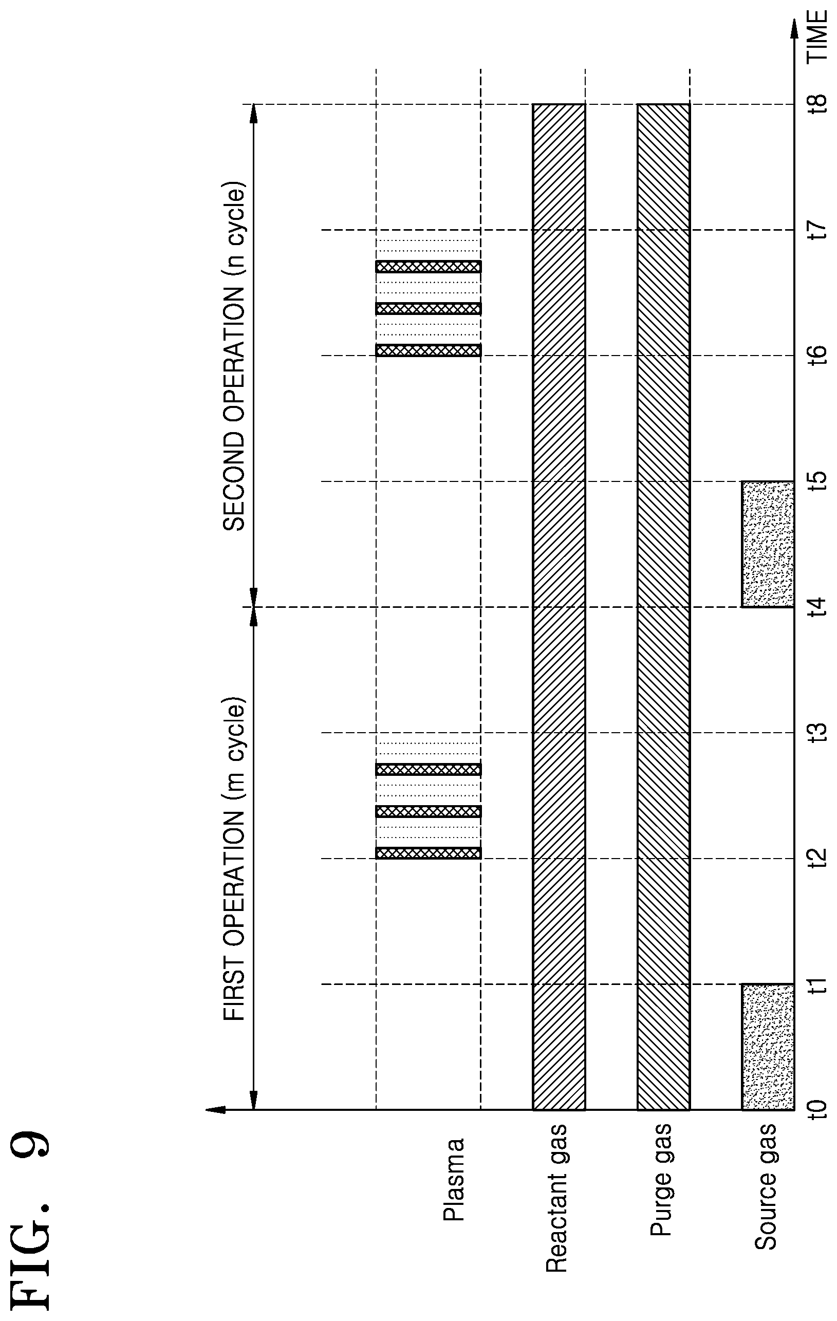
[0092] FIG. 9 is a timing diagram illustrating a thin-film deposition method according to other embodiments of the inventive concept. The thin-film deposition method according to these embodiments may be variations of the thin-film deposition method according to the above-described embodiments. Hereinafter, repeated descriptions of the embodiments will not be given herein.
[0093] Referring to FIG. 9, a thin-film deposition method capable of controlling a WER of a thin film while improving the loss amount and loss uniformity of a lower film (e.g., a pattern structure) over the entire substrate is disclosed. According to the present embodiment, before deposition of the thin film, an operation of depositing a protective film for the lower film to reduce the amount of loss of the lower film and to improve the loss uniformity is performed.
[0094] According to the present embodiment, the thin-film deposition method includes a first operation and a second operation.
[0095] The first operation is to improve the loss amount and loss uniformity of the lower film. In more detail, the first operation is for depositing a portion of the thin film which can serve as the protective film for the lower film.
[0096] The second operation is a thin-film deposition operation. In more detail, the second operation is for depositing the remaining portion of the thin film while controlling a wet etching characteristic of the thin film.
[0097] One cycle of the first operation includes a source gas supply operation, a reactant gas supply operation, and a plasma supply operation. Further, as shown in FIG. 9, the first operation may deposit a portion of the thin film by repeating (e.g., m times) this one cycle. Also, the first operation may be a plasma atomic layer deposition process.
[0098] In an embodiment, one cycle of the first operation may be sequentially performed in an order of a source gas supply operation (t0 to t1), a purge operation (t1 to t2), a reactant gas supply operation and a plasma supply operation (t2 to t3), and a purge operation (t3 to t4).
[0099] In an embodiment, process times of i) the source gas supply operation (t0 to t1), ii) the purge operation (t1 to t2), iii) the reactant gas supply operation and plasma supply operation (t2 to t3), and iv) the purge operation (t3 to t4) may be i) 0.2 seconds to 1 second, ii) 0.1 seconds to 1 second, iii) 0.1 seconds to 1 second, and iv) 0.1 seconds to 1 second, respectively.
[0100] As described later below with reference to FIG. 12, as a supply time of the source gas supply operation is increased, a loss amount of a pattern structure may be reduced and loss uniformity of the pattern structure may be improved. Thus, in an embodiment, the amount of loss and loss uniformity of the pattern structure may be controlled by controlling the supply time of the source gas supply operation of the first operation. In a preferred embodiment, the amount of loss and loss uniformity of the pattern structure may be improved by increasing the supply time of the source gas supply operation in the first operation. Preferably, the supply time of the source gas supply operation in the first operation is 0.2 seconds to 1 second.
[0101] In an alternative embodiment, a reactant gas and a purge gas may be continuously supplied to a reactor during the entire cycle. The reactant gas acts to purge the reactor together with the purge gas without reacting with a source gas when not activated by plasma. However, the reactant gas, when activated by the plasma, may be activated to chemically react with the source gas adsorbed on a substrate to form a thin film. That is, the reactant gas may act as a reactive purge gas.
[0102] Although FIG. 9 shows that the reactant gas is continuously supplied during the entire PEALD process cycle. However, in other embodiments, the reactant gas may be supplied only when the plasma is supplied, or may start to be supplied just before the plasma is supplied and may be stopped to be supplied when the plasma supply is stopped.
[0103] In other embodiments, when the reactant gas reacts with the source gas through a thermal reaction with the substrate, the reactant gas may be supplied only when the plasma is supplied and thus a thin film may be formed.
[0104] A source including silicon may be used as a source gas for silicon oxide layer deposition. In the present embodiment, an aminosilane gas is used as a source gas. An oxygen gas is used as a reaction gas and an inert gas is used as a purge gas. However, the source gas and the reactant gas described above are not limited thereto.
[0105] For example, as a silicon (Si) source, besides the aminosilane gas, TSA, (SiH3) 3N; DSO, (SiH3) 2; DSMA, (SiH3) 2NMe; DSEA, (SiH3) 2NEt; DSIPA, (SiH3) 2N (iPr); DSTBA, (SiH3) 2N (tBu); DEAS, SiH3NEt2; DTBAS, SiH3N (tBu) 2; BDEAS, SiH2 (NEt2) 2; BDMAS, SiH2 (NMe2) 2; BTBAS, SiH2 (NHtBu) 2; BITS, SiH2 (NHSiMe3) 2; TEOS, Si (OEt) 4; SiCl4; HCD, Si2Cl6; 3DMAS, SiH (N (Me) 2) 3; BEMAS, Si H2 [N (Et) (Me)] 2; AHEAD, Si2 (NHEt) 6; TEAS, Si (NHEt) 4; Si3H8; DCS, SiH2Cl2; SiHI3; SiH2I2 or the like may be used, or a combination of the above-mentioned materials and the like may be used when the Si source is supplied.
[0106] An oxygen gas may be supplied as a reactant gas. For example, an oxygen source as a reactant gas may include at least one of O.sub.3, N.sub.2O, and CO.sub.2 in addition to 02.
[0107] Furthermore, although FIG. 9 shows that the plasma of the first operation is supplied at a duty ratio of 25%, in other embodiments, the plasma may be supplied at a different duty ratio. For example, in a continuous mode, plasma is supplied onto a substrate with a duty ratio of 100%, and the magnitude of plasma power may range from 100 W to 1000 W. Meanwhile, in a pulse mode, the plasma is supplied onto the substrate at a duty ratio of 50%, and the magnitude of the plasma power may be in the range of twice the magnitude in the continuous mode, i.e., 200 W to 2000 W. Preferably, the plasma power of the plasma supply operation of the first operation is 650 W to 1200 W, and the plasma duty ratio of the plasma supply operation of the first operation is 25% to 50%.
[0108] As described above with reference to FIG. 8 and as described later below with reference to FIG. 11, the loss amount and loss uniformity of a pattern structure may be adjusted by adjusting at least one of the plasma power and the plasma duty ratio. In more detail, when increasing the power of an RF signal and decreasing a duty ratio of the RF signal while maintaining the amount of plasma power (multiplication of RF power and the duty ratio) constant, the loss amount of the pattern structure may be reduced and the loss uniformity of the pattern structure may be improved. Thus, in a preferred embodiment, the loss amount and loss uniformity of the pattern structure may be improved by adjusting at least one of the plasma power and the duty ratio of the first operation.
[0109] That is, as shown in FIG. 9, the first operation may be an operation of repeating a first cycle of applying a first RF signal in a pulse form m times while using the plasma atomic layer deposition process, and improving the loss amount and loss uniformity of the pattern structure. A source gas supply time may be increased and at least one of first RF power and the duty ratio of the first operation may be adjusted to improve the loss amount and loss uniformity of the pattern structure.
[0110] After a portion of the thin film is deposited by the first operation described above, the remaining portion of the thin film may be deposited by the second operation.
[0111] One cycle of the second operation includes a source gas supply operation, a reactant gas supply operation, and a plasma supply operation. Further, as shown in FIG. 9, the second operation may deposit the remaining portion of the thin film by repeating (e.g., n times) this one cycle. Also, the second operation may be the plasma atomic layer deposition process.
[0112] In an embodiment, one cycle of the second operation may be sequentially performed in an order of a source gas supply operation (t4 to t5), a purge operation (t5 to t6), a reactant gas supply operation and a plasma supply operation (t6 to t7), and a purge operation (t7 to t8).
[0113] In an embodiment, process times of i) the source gas supply operation (t4 to t5), ii) the purge operation (t5 to t6), iii) the reactant gas supply operation and plasma supply operation (t6 to t7), and iv) the purge operation (t7 to t8) may be i) 0.1 seconds to 1 second, ii) 0.1 seconds to 1 second, iii) 0.1 seconds to 1 second, and iv) 0.1 seconds to 1 second, respectively.
[0114] Furthermore, although FIG. 9 shows that the plasma of the second operation is supplied at a duty ratio of 25%, in other embodiments, the plasma may be supplied at a different duty ratio.
[0115] As described above with reference to FIGS. 4 to 7, the WER of the thin film may be decreased as the plasma power is increased while the plasma duty ratio is maintained constant, and the WER of the thin film may be increased by reducing the plasma duty ratio while the plasma power is maintained constant. From this, it can be seen that the WER of the thin film may be controlled by adjusting at least one of the plasma power and the plasma duty ratio to deposit the thin film. In view of the technical effect of the present disclosure, a thin film having a desired WER may be deposited by controlling at least one of the plasma power and the plasma duty ratio during the thin-film deposition operation (i.e., the second operation) in FIG. 9.
[0116] That is, as shown in FIG. 9, the second operation may be an operation of repeating a second cycle of applying a second RF power in a pulse form n times while using the plasma atomic layer deposition process, and depositing the thin film having a desired WER.
[0117] In an embodiment, the number of repetitions (m times) of the first cycle in the first operation is less than the number of repetitions (n times) of the second cycle in the second operation. Preferably, the ratio of the number of repetitions (m times) of the first cycle to the number of repetitions (n times) of the second cycle is 1/12 to 1/10.
[0118] FIG. 10 illustrates an example of process parameters that may be used when depositing a thin film on a pattern structure using the embodiments of FIG. 9.
[0119] In the present embodiment, both plasmas of the first operation and second operation are supplied in a pulse form.
[0120] A frequency of first RF plasma and second RF plasma in the first and second operations may be 27 MHz to 100 MHz, and preferably 60 MHz. In the present embodiment, the frequency of the first RF plasma and the second RF plasma is 60 MHz. Although a 60 MHz process is exemplified in the present embodiment, a higher frequency may be applied.
[0121] Deposition of the thin film may be performed at a temperature ranging from room temperature to 500.degree. C., and preferably at room temperature to 100.degree. C. In the present embodiment, the deposition of the thin film is performed at a process temperature of 50.degree. C.
[0122] In a preferred embodiment, plasma power of the plasma supply operation in the first operation is greater than plasma power of the plasma supply operation in the second operation, and a plasma duty ratio of the plasma supply operation in the first operation is less than a plasma duty ratio of the plasma supply operation in the second operation. This is because the purpose of the first operation is to improve a loss amount and loss uniformity of the pattern structure and the loss amount and loss uniformity of the pattern structure are improved as the plasma power increases and the duty ratio decreases in the first operation. In the present embodiment, the power of a first RF signal of the first operation is 1200 W, and the duty ratio is 25%. The power of a second RF signal in the second operation is 900 W, and the duty ratio is 37%.
[0123] In the present embodiment, process times of the source gas supply operation, the purge operation, the reactant gas supply operation and plasma supply operation, and the purge operation in the first operation are respectively 1 second, 0.3 seconds, 0.3 seconds, and 0.2 seconds, and process times of the source gas supply operation, the purge operation, the reactant gas supply operation and plasma supply operation, and the purge operation in the second operation are respectively 0.2 seconds, 0.3 seconds, 0.3 seconds, and 0.2 second.
[0124] In a preferred embodiment, a supply time of the source gas supply operation in the first operation is longer than a supply time of the source gas supply operation in the second operation. This is to enhance the function of a protective film for a lower film (e.g., an SOH film) by sufficiently supplying the source gas in the first operation. This will be described later below with reference to FIG. 12. Preferably, the supply time of the source gas supply operation in the first operation is two to five times the supply time of the source gas supply operation in the second operation. Preferably, the supply time of the source gas supply operation in the first operation is in the range of 0.2 seconds to 1 second. In the present embodiment, the source gas supply time in the first operation is 1 second, which is five times longer than 0.2 seconds, which is the source gas supply time in the second operation.
[0125] In the present embodiment, the first operation is performed 10 times and the second operation is performed 120 times. In this case, a ratio of the number of repetitions of the first operation to the number of repetitions of the second operation is 1/12.
[0126] FIG. 11 is a graph showing the degree of loss of a lower mask (i.e., an SOH) generated when a thin-film deposition method according to embodiments of the inventive concept is performed. FIG. 11 is a graph illustrating an SOH loss amount depending on a substrate position, which is generated when plasma is supplied onto a substrate in a continuous mode and a pulse mode in a first operation. Plasma power and a duty ratio are changed while maintaining the amount of plasma power (a multiplier value (multiplication) of RF power and a duty ratio) supplied during the plasma supply operation in the first operation, and the degree of SOH loss is measured.
[0127] The horizontal axis in FIG. 11 indicates a distance from the center portion of a substrate with a diameter of 300 mm. That is, the center of the horizontal axis in FIG. 11 denotes the center portion of the substrate with a diameter of 300 mm. A vertical axis in FIG. 11 indicates a loss amount of a pattern structure (SOH film in this case) during thin-film deposition. That is, each of the left and right sides of the center of the horizontal axis (0 mm) of FIG. 11 indicates the degree of SOH loss according to a position in half the length of the substrate (that is, a length of 150 mm).
[0128] In FIG. 11, CW indicates a continuous wave RF mode and further indicates a conventional RF pulsing mode with a duty ratio of 100%. D is a duty ratio and indicates a time during which actual plasma is supplied during the entire plasma supply time. For example, D50 means that plasma is supplied only for 50% of the plasma supply time.
[0129] FIG. 11 shows an experimental result of measuring an SOH loss amount while varying power and a duty ratio of a first RF signal in the first operation among the process parameters shown in FIG. 10. The first operation is performed 10 times, the second operation is performed 120 times, and process times of the first operation (source supply/purge/plasma apply/purge) are 1.0/0.3/0.3/0.2 seconds, respectively.
[0130] Referring to FIG. 11, it can be seen that when a certain amount of power (in this case, 300 W.times.0.3 s.times.100%=90 Ws) is applied in a continuous mode, an SOH located at the periphery portion of a substrate is relatively less lost while an SOH located at the center portion of the substrate is relatively more lost. That is, it can be seen that when plasma is continuously applied during the first operation, the loss amount of the pattern structure is large and the loss does not occur uniformly over the entire substrate.
[0131] It can be seen that damage to the SOH as a whole is reduced when a power amount (in this case, 650 W.times.0.3 s.times.50%=97.5 Ws) similar to that in the continuous mode is applied in the pulse mode having a duty ratio of 50%. Also, it can be seen that although damage to the SOH located at the center portion of the substrate is relatively high and damage to the SOH located at the periphery portion of the substrate is relatively low, a deviation of the SOH damage as a whole decreases.
[0132] It can be seen that SOH loss is further reduced when the same amount of power (in this case, 1200 W.times.0.3 s.times.25%=90 Ws) as that in the continuous mode is applied in the pulse mode having a duty ratio of 25%, and a deviation between the amount of loss of an SOH located at the center portion of the substrate and the amount of loss of an SOH located at the periphery portion of the substrate is further reduced.
[0133] It can be seen from FIG. 11 that as a duty ratio decreases and a supplied plasma power increases, the amount of loss of a mask pattern (in this case, SOH) is reduced and SOH loss uniformity is improved.
[0134] As such, according to the embodiments of the inventive concept, in a plasma supply operation, it is possible to prevent a hard mask from being damaged unevenly by applying a relatively large amount of power in comparison with power supplied during a continuous mode for a relatively short time. As a result, a mask formed by a residual spacer may have a uniform inner space CD and an outer space CD, and features may be aligned so that the yield of the final product may be improved and good characteristics of the product may be achieved.
[0135] FIG. 12 is a table of SOH loss uniformity and a WER of a thin film according to a source supply time in a first operation.
[0136] In more detail, FIG. 12 shows results of measuring the SOH loss uniformity in the first operation and the WER of the thin film after the second operation while changing only a process time of a source gas supply operation in the first operation among the process parameters shown in FIG. 10. In the present embodiment, the first and second operations proceed in-situ.
[0137] Conditions 1 to 4 are all the same except that a different amount of source gas is supplied in the first operation. A source gas supply time in the first operation is 0.2 seconds in condition 1, 0.4 seconds in condition 2, 0.6 seconds in condition 3, and 1 second in condition 4.
[0138] Referring to FIG. 12, it can be seen that as the source gas supply time increases, the SOH loss uniformity (the amount of loss at a position where the maximum loss occurs--the amount of loss at a position where the minimum loss occurs) decreases. This is because the function of a protective film for a lower SOH film is strengthened by sufficiently supplying a source gas. It can be seen from this that, in addition to plasma power and a duty ratio in the first operation, the source gas supply time (or the amount of source gas supply) is also an important process variable that can reduce the amount of loss of a lower mask pattern. Therefore, by controlling the source gas supply time in the first operation, a loss amount and loss uniformity of a lower film may be adjusted to a desired level.
[0139] Furthermore, referring to FIG. 12, in all of the conditions 1 to 4, it can be seen that the WER of the thin film spans the range of a target WER (106 .ANG./min to 108 .ANG./min). As described above with reference to FIG. 7, by controlling the plasma power and the duty ratio in the second operation, a thin film having a desired WER may be deposited.
[0140] As such, according to the embodiments of the inventive concept, the loss amount and loss uniformity of the lower film (i.e., a pattern structure) may be adjusted by controlling at least one of the source gas supply time of the source gas supply operation, plasma power of a plasma supply operation, and a plasma duty ratio of a plasma supply operation in the first operation. Further, a thin film having a desired WER may be deposited by controlling at least one of the plasma power of the plasma supply operation and the plasma duty ratio of the plasma supply operation in the second operation. In other words, according to the embodiments of the inventive concept, it is possible to deposit a thin film having a desired etching characteristic while adjusting the loss amount and loss uniformity of the lower film to a desired level at the time of thin-film deposition.
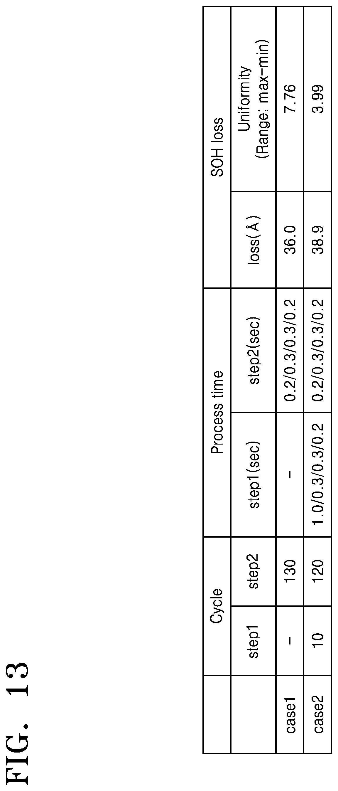
[0141] FIG. 13 is a table comparing SOH loss amount and SOH loss uniformity in a case where a first operation, which is to improve a loss amount and loss uniformity of a lower film, is performed and in a case where the first operation is not performed.
[0142] In Case 1, a thin film is deposited by performing a second operation 130 times without the first operation. In Case 2, the thin film is deposited by performing the first operation 10 times and the second operation 120 times. In both cases, the total cycles are 130 cycles. Process conditions of Case 1 and Case 2 are the same as the process conditions shown in FIG. 10.
[0143] Referring to FIG. 13, when only the second operation is performed (Case 1), the SOH loss uniformity is 7.76, whereas, when the first operation is performed before the second operation (Case 2), the SOH loss uniformity is 3.99. That is, it can be seen that the SOH loss uniformity is improved by about 50% by performing the first operation before performing the second operation.
[0144] It can be seen from this that the loss amount and loss uniformity of the lower film (SOH film in this case) may be improved by performing the first operation. That is, during an initial process of thin-film deposition, the loss amount and loss uniformity of the lower film may be improved by increasing a source gas supply time and plasma power and reducing a plasma duty ratio to perform a plasma atomic layer deposition process.
[0145] This technical advantage of the present disclosure may be more clearly understood by referring to FIGS. 14 to 18. FIGS. 14 to 18 are cross-sectional views illustrating a method of manufacturing a semiconductor device according to the other embodiments of the inventive concept. The method of manufacturing the semiconductor device according to these embodiments may use the thin-film deposition method according to the above-described embodiments. Hereinafter, repeated descriptions of the embodiments will not be given herein.
[0146] Referring to FIG. 14, a first layer 110, which is a film to be etched, is formed on a substrate 100. The film to be etched may be an insulating layer such as a silicon oxide layer or a mask layer such as an amorphous carbon layer (ACL) used for patterning a lower layer.
[0147] Thereafter, a second layer 120 is formed on the first layer 110. The second layer 120 may be formed of a polymeric material that can be easily removed through an ashing and/or strip process as a hard mask. For example, the second layer may 120 include an SOH film or a C--SOH film. The second layer 120 is then patterned to expose at least a portion of the first layer 110. Accordingly, the substrate 100 including a thin film of the first layer 110 as a film to be etched and a first mask pattern 120 formed on the thin film may be provided.
[0148] Referring to FIG. 15, a portion 130a of a third layer is formed on an exposed surface of the first layer 110 and the second layer 120 (i.e., with respect to a semiconductor substrate and a pattern structure). The forming of the portion 130a of the third layer may be performed using the operation of improving the loss amount and loss uniformity of the pattern structure in the thin-film deposition method according to the above-described embodiments (i.e., the first operation of FIGS. 9 and 10).
[0149] In more detail, the portion 130a of the third layer may be deposited by repeating a first cycle in which a first RF signal is applied in a pulse form a certain number of times (e.g., m times) while using a PEALD process.
[0150] As described above, during this operation, the loss amount and loss uniformity of a sub-layer film (in this case, the second layer 120) may be improved by increasing a source gas supply time and plasma power and decreasing a plasma duty ratio.
[0151] Thereafter, referring to FIG. 16, a remaining portion 130b of the third layer is formed with respect to the semiconductor substrate and the pattern structure. The forming of the remaining portion 130b of the third layer may be performed using the film deposition operation in the thin-film deposition method according to the above-described embodiments (i.e., the second operation of FIGS. 9 and 10).
[0152] In more detail, the remaining portion 130b of the third layer may be deposited by repeating a second cycle in which second RF power is applied in a pulse form a certain number of times (e.g., n times) while using the PEALD process. Here, the third layer includes the portion 130a of the third layer of FIG. 15 and the remaining portion 130b of the third layer of FIG. 16.
[0153] As described above, during this operation, a WER of a thin film (in this case, the remaining portion 130b of the third layer) may be controlled by controlling at least one of plasma power and a plasma duty ratio of a plasma supply operation. In more detail, the WER of the third layer may be reduced by maintaining the plasma duty ratio constant and increasing the plasma power or by maintaining the plasma power constant and increasing the plasma duty ratio.
[0154] In the present embodiment, the first operation is performed 10 times and the second operation is performed 120 times. Thus, as shown in FIG. 16, a thickness of the portion 130a of the third layer deposited during the first operation is less than a thickness of the remaining portion 130b of the third layer deposited during the second operation.
[0155] Referring to FIG. 17, at least a portion of the third layer is removed to form a spacer pattern 135 of the third layer. For example, a wet etching process for the third layer is performed so that a spacer pattern 135 may be formed by etching back the third layer formed on the second layer (the first mask pattern 120).
[0156] As described above, since loss uniformity of the second layer 120 is improved by the present disclosure, the spacer pattern 135 of the third layer may have a constant linewidth size over the substrate 100.
[0157] Referring to FIG. 18, thereafter, the second layer is removed. Therefore, a DPT process of etching the first layer 110, which is a film to be etched, may be performed using the remaining spacer pattern 135 of the third layer as a mask.
[0158] As such, according to the embodiments of the inventive concept, during an initial process of thin-film deposition, a source gas is sufficiently supplied and plasma is applied in a pulse mode, thereby the problem of damaging an SOH mask pattern (i.e., the first mask pattern 120) used to form a spacer mask pattern (i.e., the spacer pattern 135 of FIG. 18) of a DPT process may be avoided. Further, as described above, during the initial process of thin-film deposition, the source gas is sufficiently supplied and high-frequency plasma is applied in a pulse mode, and in particular power greater than power supplied during a continuous mode is applied for a relatively short period of time, thereby the loss uniformity of a hard mask (first mask pattern) of the DPT process may be improved. That is, a mask formed by a residual spacer may have a uniform inner space CD and an outer space CD. As a result, after an etch-back process of the DPT process, a more uniform spacer mask (in this case, the spacer pattern 135 in FIG. 18) may be formed so that the yield of the final product may be improved and good characteristics of the product may be achieved.
[0159] Furthermore, according to the embodiments of the inventive concept, during a thin-film deposition process, a thin film having a desired etching characteristic may be deposited by applying plasma in a pulse mode and by controlling power and a duty ratio of the plasma.
[0160] As described above, according to the embodiments of the inventive concept, it is possible to deposit a thin film having a desired etching characteristic while adjusting a loss amount and loss uniformity of a lower film to a desired level by performing a thin-film deposition process in two step operations with different process conditions. When the thin-film deposition method according to the inventive concept is applied to the DPT process, a more uniform spacer mask may be formed over the entire substrate.
[0161] It is to be understood that the shape of each portion of the accompanying drawings is illustrative for a clear understanding of the present disclosure. It should be noted that the portions may be modified into various shapes other than the shapes shown.
[0162] While one or more embodiments have been described with reference to the figures, it will be understood by those of ordinary skill in the art that various changes in form and details may be made therein without departing from the spirit and scope of the disclosure as defined by the following claims.
* * * * *
D00000
D00001
D00002
D00003
D00004
D00005
D00006
D00007
D00008
D00009
D00010
D00011
D00012

XML
uspto.report is an independent third-party trademark research tool that is not affiliated, endorsed, or sponsored by the United States Patent and Trademark Office (USPTO) or any other governmental organization. The information provided by uspto.report is based on publicly available data at the time of writing and is intended for informational purposes only.
While we strive to provide accurate and up-to-date information, we do not guarantee the accuracy, completeness, reliability, or suitability of the information displayed on this site. The use of this site is at your own risk. Any reliance you place on such information is therefore strictly at your own risk.
All official trademark data, including owner information, should be verified by visiting the official USPTO website at www.uspto.gov. This site is not intended to replace professional legal advice and should not be used as a substitute for consulting with a legal professional who is knowledgeable about trademark law.