Magnetic Field Sensor Using Acoustically Driven Ferromagnetic Resonance
SALAHUDDIN; SAYEEF ; et al.
U.S. patent application number 16/464066 was filed with the patent office on 2019-12-19 for magnetic field sensor using acoustically driven ferromagnetic resonance. The applicant listed for this patent is THE REGENTS OF THE UNIVERSITY OF CALIFORNIA. Invention is credited to DOMINIC E. LABANOWSKI, SAYEEF SALAHUDDIN.
| Application Number | 20190385586 16/464066 |
| Document ID | / |
| Family ID | 62559205 |
| Filed Date | 2019-12-19 |


View All Diagrams
| United States Patent Application | 20190385586 |
| Kind Code | A1 |
| SALAHUDDIN; SAYEEF ; et al. | December 19, 2019 |
MAGNETIC FIELD SENSOR USING ACOUSTICALLY DRIVEN FERROMAGNETIC RESONANCE
Abstract
An acoustically driven ferromagnetic resonance (ADFMR) device includes a piezoelectric element, a pair of transducers arranged to activate the piezoelectric element to generate an acoustic wave, a magnetostrictive element arranged to receive the acoustic wave, and a readout circuit to detect one of either a change in the magnetostrictive element or a change in the acoustic wave.
| Inventors: | SALAHUDDIN; SAYEEF; (Walnut Creek, CA) ; LABANOWSKI; DOMINIC E.; (Berkeley, CA) | ||||||||||
| Applicant: |
|
||||||||||
|---|---|---|---|---|---|---|---|---|---|---|---|
| Family ID: | 62559205 | ||||||||||
| Appl. No.: | 16/464066 | ||||||||||
| Filed: | December 11, 2017 | ||||||||||
| PCT Filed: | December 11, 2017 | ||||||||||
| PCT NO: | PCT/US17/65607 | ||||||||||
| 371 Date: | May 24, 2019 |
Related U.S. Patent Documents
| Application Number | Filing Date | Patent Number | ||
|---|---|---|---|---|
| 62434122 | Dec 14, 2016 | |||
| Current U.S. Class: | 1/1 |
| Current CPC Class: | G01R 33/1284 20130101; B06B 1/06 20130101; G01R 33/18 20130101; G01R 33/0325 20130101; G10K 11/36 20130101; G01R 33/096 20130101; G01R 33/0327 20130101; G01R 33/075 20130101 |
| International Class: | G10K 11/36 20060101 G10K011/36; G01R 33/18 20060101 G01R033/18 |
Goverment Interests
GOVERNMENT SUPPORT
[0002] This invention was made with government support under Grant Number 1160504 awarded by the National Science Foundation. The government has certain rights in the invention.
Claims
1. An acoustically driven ferromagnetic resonance (ADFMR) device, comprising: a piezoelectric element; a pair of transducers arranged to activate the piezoelectric element to generate an acoustic wave; a magnetostrictive element arranged to receive the acoustic wave, wherein the acoustic wave resonates at a ferromagnetic resonance of the magnet; and a readout circuit to detect one of either a change in the acoustic wave caused by the magnetostrictive element or a change in the magnetostrictive element.
2. The ADFMR device of claim 1, wherein the piezoelectric element comprises a piezoelectric substrate.
3. The ADFMR device of claim 2, wherein the piezoelectric substrate comprises a Y-cut lithium niobate substrate.
4. The ADFMR device of claim 1, further comprising a spacer residing on the magnetostrictive element.
5. The ADFMR device of claim 1, further comprising an antiferromagnet residing on the magnetostrictive element.
6. The ADFMR device of claim 2, wherein the transducers comprise interdigitated transducers arranged on the piezoelectric substrate, wherein one of the pair of interdigitated transducers is an input interdigitated transducer and another of the pair is an output interdigitated transducer; and the magnetostrictive element resides between the input and output interdigitated transducers.
7. The ADFMR device of claim 6, further comprising a voltage source connected to the input interdigitated transducer.
8. The ADFMR device of claim 1, further comprising a substrate having a cavity, wherein: a first transducer of the pair of transducers resides on the substrate and suspended at least partially over the cavity; the piezoelectric element comprises two piezoelectric elements and a first piezoelectric element of the two piezoelectric elements resides on the first transducer; the magnetostrictive element resides on the first piezoelectric component; a second of the two piezoelectric elements resides of the magnetostrictive element; and a second transducer of the pair of transducers resides on the second piezoelectric elements.
9. The ADFMR device of claim 1, further comprising a substrate having a cavity, wherein: a first transducer of the pair of transducers residing on the substrate at least partially suspended over the cavity; the piezoelectric element resides on the first transducer; a second transducer of the pair of transducers residing on the piezoelectric element; and the magnetostrictive element arranged adjacent one of the pair of transducers, on an opposite side of the transducer from the piezoelectric element.
10. The ADFMR device of claim 1, further comprising a substrate, wherein: a first transducer of the pair of transducers on the substrate; the piezoelectric element residing on the first transducer; and a second transducer of the pair of transducers residing on the piezoelectric element.
11. The ADFMR device of claim 10, wherein the piezoelectric element comprises two piezoelectric elements and the magnetostrictive element resides between the two piezoelectric elements.
12. The ADFMR device of claim 10, wherein the magnetostrictive element resides on the piezoelectric element, an oxide pad resides on the magnetostrictive element, and the second transducer resides on the oxide pad.
13. The ADFMR device of claim 10, wherein the magnetostrictive element resides on a side of the substrate opposite the pair of transducers and the piezoelectric element.
14. A method of operating a sensor, comprising: applying a signal to one of a pair of transducers arranged adjacent a piezoelectric element to cause the piezoelectric element to generate an acoustic wave that passes through a magnetostrictive element, wherein the acoustic wave is at a ferromagnetic resonance of the magnetostrictive element; measuring one of either a change in the magnetostrictive element or a change in the acoustic wave; and comparing the change in the magnetostrictive element to determine a magnetic field experienced at the magnetostrictive element.
15. The method of claim 14, wherein applying the signal to an input transducer comprises applying the signal to one of the pair of interdigitated transducers, such that the signal passes through a magnetostrictive element to an output transducer of the pair; measuring an output signal at the output transducer; comparing the output signal to the input signal to determine the magnetic field experienced at the magnetostrictive element.
16. The method of claim 15, wherein the one of the pair of interdigitated transducers generates a surface acoustic wave on a piezoelectric substrate upon which the pair of interdigitated transducers resides.
17. The method of claim 14, wherein applying the signal to one of the pair of transducers comprises applying a signal to one of the pair of transducers arranged on opposite sides of a piezoelectric element, wherein the magnetostrictive element resides adjacent one of the transducers.
Description
CROSS REFERENCE TO RELATED APPLICATION
[0001] This application claims priority to and the benefit of U.S. Provisional Application No. 62/434,122 filed Dec. 14, 2016, which is incorporated herein by reference in its entirety
BACKGROUND
[0003] Ferromagnetic resonance (FMR) measures magnetic properties of materials by detecting the precessional motion in of the magnetization in a ferromagnetic sample. Different types of FMR include externally-driven FMR and current-driven FMR. FMR can be excited using a variety of techniques, like cavity excitation, stripline excitation, spin transfer torque, and spin orbit torque, among others These applications are typically not compatible with device applications. They require large cavities, high power drive and use large sample volume in order to be effective.
[0004] However, FMR has some attractive characteristics. These includes the ability to modulate material permeability and electromagnetic absorption as a function of magnetic applied field.
BRIEF DESCRIPTION OF THE DRAWINGS
[0005] FIG. 1 shows a block diagram an embodiment of an acoustically driven ferromagnetic resonance device.
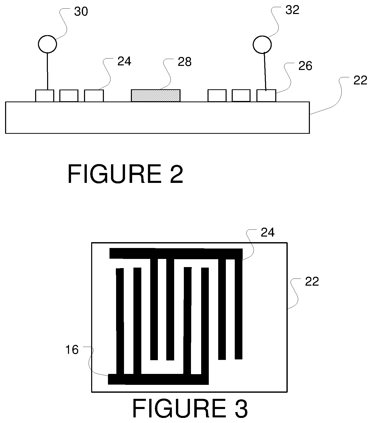
[0006] FIG. 2 shows an embodiment of an acoustically driven, surface acoustic wave, ferromagnetic resonance (ADFMR) device.
[0007] FIG. 3 shows a top view of interdigitated transducers used in a surface acoustic wave ADFMR device.
[0008] FIG. 4 shows a top view of an ADFMR device with an exploded view of interdigitated transducers.
[0009] FIGS. 5 and 6 shows graphs of absorption for an ADFMR device.
[0010] FIGS. 7-11 show embodiments of an ADFMR device as a film bulk acoustic resonator (FBAR).
[0011] FIGS. 12-16 show embodiments of an ADFMR device in a high-tone bulk acoustic resonator (HBAR).
[0012] FIGS. 17-19 show embodiments of an ADFMR device having a structure on the magnetostrictive element.
DETAILED DESCRIPTION OF THE EMBODIMENTS
[0013] FIG. 1 shows a block diagram of an embodiment of an acoustically driven ferromagnetic device (ADFMR) 10. These devices may be used as field sensors by measuring transmitted power, among many other applications. The acoustic drive portion 12 of the device may consist of one of many different types of acoustic resonators, including surface acoustic wave (SAW) resonators, film bulk acoustic resonators (FBAR), and high-tone bulk acoustic resonators (HBAR).
[0014] The acoustic drive portion generates an acoustic wave at or near the ferromagnetic resonance of a magnetostrictive element, discussed in more detail below. As used here the phrase `at the ferromagnetic resonance` includes a reasonable variation from the exact ferromagnetic resonance of the magnetostrictive element. The region of ferromagnetic resonance considered to be `at the ferromagnetic resonance` is the region in which the FMR-related absorption is greater than 10%, approximately 0.4 dB. In addition, for purposes of this discussion and scope of the claims, the term `ferromagnetic resonance` includes spin wave resonance. In addition, the acoustic drive portion generates the acoustic wave at a high enough frequency to reach the resonance range, typically in the 100s of MHz to GHz range.
[0015] Typically, the acoustic drive portion consists of at least one, but typically a pair of, transducers, such as electrodes, that activate a piezoelectric element to generate waves. A magnetostrictive element 14 receives the wave as a signal and changes its properties in response to the received wave. Detection circuitry 16 detects the change in the property of the magnetostrictive element and that change is used to determine a result. The detection circuitry may also measure the change in the wave generated by the acoustic drive portion 12.
[0016] FIG. 2 shows a side view of an acoustically driven ferromagnetic resonance (ADFMR) device, using interdigitated transducers on a piezoelectric substrate with a magnetostrictive ferromagnet deposited between them. Application of an AC voltage to one of the transducers generates a coherent, elastic wave that travels along the surface of the substrate. The surface acoustic wave (SAW) interacts with the magnetic element via the magnetoelastic interaction and provides the radio frequency (RF) driving field necessary to excite the magnet into resonance.
[0017] One important feature of ADFMR devices lies in the fact that it is a voltage-driven effect, and thus is suitable for low-power applications. Since the piezoelectric generations of SAWs is based on the strength of the applied electric field, as opposed to electron flow through the device, ADFMR devices can operate with very low power dissipation. Experiments have found that significant power absorption, greater than 70 dB, can be realized in such structures. This indicates that coupling strength between the magnetic and acoustic waves is extremely strong. These experiments have also shown that the power absorption scales with increase in film thickness, and the behavior remains consist for a large range of input powers.
[0018] Generally, the device 20 consists of a substrate 22. In one embodiment, the substrate consists of a Y-cut lithium niobate substrate. These devices use a double-electrode interdigitated transducer (IDT) 24 and 26. IDTs can effectively excite surface acoustic waves (SAWs). The double electrode IDTs in this embodiment excite at high harmonics. Normal IDTs also can excite at high harmonics, but suffer from much worse performance. The double electrode design reduces destructive interference cause by reflections with the IDT when operating at higher-order modes by replacing a structure of alternating signal and ground electrodes with one where each signal and ground electrode is replaced by a pair of electrodes with a gap between them. The IDTs are aligned so that the direction of propagation of the SAWs would be along the z-axis of the lithium niobate substrates which allows for all devices to operate the same fundamental frequency and with a consistent SAW mode. FIG. 3 shows a plan view of the IDTs.
[0019] The IDTs are fabricated using multi-step optical lithography. In one embodiment, after the IDT patterning is performed, contacts are formed. In one embodiment, 70 nm of aluminum was deposited via thermal evaporation and a liftoff was performed to create the contacts. A second photolithography step with alignment may be performed to define the magnet regions 28 between the electrodes 24 and 26. In one embodiment, the magnet region consists of nickel. FIG. 4 shows an embodiment of the substrate 22 having a nickel film 18. The electrode 24 is also shown in an exploded view to the right side of the figure.
[0020] In operation, a radio frequency field is applied to one of the IDTs using a voltage source 30. In one embodiment, an AC voltage usually in the gigahertz range is applied to one of these IDTs to create a coherent elastic wave that travels along the surface of the piezoelectric. The time varying strain caused by the SAW is transferred to the element consisting of magnetostrictive material 28, which changes its crystalline anisotropy. The magnetostrictive element 28 may consist of ferromagnetic material, ferrimagnetic material, etc. The SAW interacts with the magnetostrictive element via the magnetoelastic interaction and provides the RF driving field necessary to excite the magnet into resonance. This drives the magnetostrictive element into ferromagnetic resonance. Power absorbed by the magnet can be calculated by reading out the amplitude of the attenuated SAW at the second IDT at 32.
[0021] By normalizing the input power and accounting for differing losses at various input frequencies, the devices demonstrate that the relative magnitude of ADMR absorption increases with increased frequency. This is shown in FIG. 5. This result confirms that the power absorption trend seen in ADFMR matches that of the convention FMR in thin films. FIG. 6 shows the relative absorption against power at the magnetic element.
[0022] In application, the magnetostrictive element begins to strongly absorb the traveling SAW applied to the input IDT and transmitting through the input IDT to the output IDT through the magnetostrictive element. This allows measuring the absorption of the SAW by comparing the input power incident on the generating or input IDT to the power measured on the detection or output IDT. It can be determined whether the magnet has entered FMR and leads to a determination of the magnetic field experienced at the magnetostrictive element.
[0023] This effect can be used as an extremely sensitive magnetic field sensor by biasing the magnetic film so that it is very close to entering FMR and then measuring the absorption and/or phase of the SAWs as a function of applied magnetic field. Residing in the Earth's ambient magnetic field, or a zero-magnetic field, puts the sensor close enough to resonance to be used for sensing. This bias can be achieved by using exchange bias, putting an antiferromagnet on top or bottom, or by using dipolar coupling, such as putting another magnetic layer nearby.
[0024] Very small changes in the external magnetic field can cause substantial and easily measurable changes in the output power and output phase measurements on the detection IDT. By using industry-standard generation and detection techniques and an input power of 20 mW, the devices will be able to measure magnetic fields on the order of 100 femtoTesla at room temperatures. This beats comparable state of the art devices by several orders of magnitude when considering relevant SWaP metrics.
[0025] In the ADFMR embodiments above, the detection circuitry comprises the second transducer and a voltage reader to read out the voltage detected at the second transducer. Other types of detection circuitry may include anisotropic magnetoresistance, in which the detection circuitry measures the resistance of the magnet. Other means of detection include detecting the spin Hall effect by placing a metal that exhibits the spin Hall effect, typically a heavy metal like platinum, on top of, or adjacent to, the magnet and read out the generated voltage. Other forms include optical readout via the magneto-optic Kerr effect. As will be discussed below, one-port resonators like high-tone bulk acoustic resonators (HBAR) and film bulk acoustic resonators (FBAR), the circuitry would measure the impedance of the resonator or the reflection of the signal in the magnet, instead of the transmission at the magnet as done in the SAW geometry.
[0026] FIG. 7 shows a prior art example of a FBAR 40. Generally, these devices constitute a cavity in a substrate 42. A first electrode 44 is suspended over the cavity. A piezoelectric (PZT) element 48 resides on the first electrode, suspended over the cavity, and a second electrode 46 resides on the PZT. Generally, once voltage is applied to one of the electrodes, the PZT vibrates and generates an acoustic wave that resonates in the cavity.
[0027] Typically, the strain is highest in the middle of the PZT vertically, so one would want to locate the magnetostrictive element, referred to here as a magnet, near high point of the strain. An embodiment of such a device 50 having a magnetostrictive element is shown in FIG. 8. The substrate 52 has a cavity, as in the device of FIG. 7, electrodes 54 and 56 and a piezoelectric element 58. In this embodiment, the PZT element is divided into two parts with the magnet 60 between them. Other architectures are of course possible.
[0028] FIG. 9 shows an alternative architecture, in which the magnet 60 resides between the first electrode 54 and the PZT element 58. FIG. 10 shows an embodiment in which the magnet 60 resides outside the electrodes 54 and 56, in either position 60a or 60b. FIG. 11 shows a symmetric structure as in FIG. 8, but the opposite of the magnet 60 from the PZT 58 is a spacer, such as an oxide spacer 62. One should note that the spacer may consist of many different materials, oxide is merely one example.
[0029] Alternative acoustic resonators could include high-tone bulk acoustic resonators (HBAR). These devices typically consist of a substrate without a cavity, and the generated acoustic waves either propagate through the substrate or on the surface. FIG. 12 shows a prior art example of such a device. A first electrode 74 resides on the substrate 72, and the PZT element 78 resides between the first electrode 74 and the second electrode 76. Note that the electrodes may also be referred to as transducers. The strain wave has a sinusoidal profile in the substrate.
[0030] In the embodiments using magnetostrictive elements for detection, the magnet 90 may be placed outside the electrodes as shown in FIG. 13, or in a stack between two pieces of the PZT element 88 as shown in FIG. 14. Other architectures include the magnet 90 in a stack with the PZT 88 and an oxide spacer 92 between the magnet 90 and the second electrode 86 as in FIG. 15. In yet another alternative, the magnet 90 may be located outside the electrodes, and on the opposite surface of the substrate from the electrodes-PZT stack as shown in FIG. 16.
[0031] One modification that may occur in any of the device architectures includes a spacer or other structure on the magnetostrictive element. The use of a spacer maximizes the strain on the magnetostrictive element. This may apply to any of the architectures previously discussed, including the FBAR, HBAR and the structure with the IDTs. Adaptations for the FBAR and HBAR structures are shown in FIGS. 17-19.
[0032] FIG. 17 shows an embodiment of an FBAR structure having the substrate 93 with the cavity, a first electrode 94, second electrode 96 and the PZT element 98 between them. In this particular structure, the magnet 100 resides on the upper electrode 96. The spacer 102 then resides between the magnet and the air.
[0033] FIG. 18 shows a similar variation for the HBAR structure in which the magnet 100 resides on the upper electrode 96 and the substrate 93 does not have a cavity. The spacer 102 resides on the top of the magnet, between the magnet 100 and the air. Similarly, the structure of FIG. 19 has the magnet on the surface of the substrate 93 opposite the surface upon which the lower electrode 94 resides. The spacer 100 resides on the surface of the magnet 100 that would otherwise be exposed to air.
[0034] Other variations of the structure could exchange the spacer 102 for a antiferromagnet used for biasing. Additionally, the spacer could be replaced with a heavy metal used as part of the detection circuitry, as mentioned above.
[0035] In summary, the device may consist of acoustically driven ferromagnetic devices includes SAW resonators, HBARs and FBARs. The piezoelectric element may be a PZT material activated by electrodes acting as transducers, or it may consist of the substrate upon which the transducers reside. The detection circuitry may detect a change in the power absorption at the readout one of the transducers, or it may detect anisotropic magnetoresistance, inverse spin Hall effect, optical readout, the impedance of the resonator, or reflection of the signal, among many others. Other possibilities include tunneling magnetoresistance, anomalous Hall effect, and giant magnetoresistance.
[0036] It will be appreciated that variants of the above-disclosed and other features and functions, or alternatives thereof, may be combined into many other different systems or applications. Various presently unforeseen or unanticipated alternatives, modifications, variations, or improvements therein may be subsequently made by those skilled in the art which are also intended to be encompassed by the following claims.
* * * * *
D00000
D00001
D00002
D00003
D00004
D00005
D00006
D00007
D00008
D00009
D00010
D00011
D00012

XML
uspto.report is an independent third-party trademark research tool that is not affiliated, endorsed, or sponsored by the United States Patent and Trademark Office (USPTO) or any other governmental organization. The information provided by uspto.report is based on publicly available data at the time of writing and is intended for informational purposes only.
While we strive to provide accurate and up-to-date information, we do not guarantee the accuracy, completeness, reliability, or suitability of the information displayed on this site. The use of this site is at your own risk. Any reliance you place on such information is therefore strictly at your own risk.
All official trademark data, including owner information, should be verified by visiting the official USPTO website at www.uspto.gov. This site is not intended to replace professional legal advice and should not be used as a substitute for consulting with a legal professional who is knowledgeable about trademark law.