Substrate Processing Method And Device Manufactured By Using The Same
Min; Yoon Ki
U.S. patent application number 16/421339 was filed with the patent office on 2019-11-28 for substrate processing method and device manufactured by using the same. The applicant listed for this patent is ASM IP Holding B.V.. Invention is credited to Yoon Ki Min.
| Application Number | 20190363006 16/421339 |
| Document ID | / |
| Family ID | 68614127 |
| Filed Date | 2019-11-28 |


View All Diagrams
| United States Patent Application | 20190363006 |
| Kind Code | A1 |
| Min; Yoon Ki | November 28, 2019 |
SUBSTRATE PROCESSING METHOD AND DEVICE MANUFACTURED BY USING THE SAME
Abstract
Provided are a substrate processing method and a device manufactured by using the same, which may improve etch selectivity of an insulating layer deposited on a stepped structure. The substrate processing method includes: forming a first layer on a stepped structure having an upper surface, a lower surface, and a side surface connecting the upper surface and the lower surface; weakening at least a portion of the first layer; forming a second layer on the first layer; and performing an isotropic etching process on the first layer and the second layer.
| Inventors: | Min; Yoon Ki; (Dongjak-gu, KR) | ||||||||||
| Applicant: |
|
||||||||||
|---|---|---|---|---|---|---|---|---|---|---|---|
| Family ID: | 68614127 | ||||||||||
| Appl. No.: | 16/421339 | ||||||||||
| Filed: | May 23, 2019 |
| Current U.S. Class: | 1/1 |
| Current CPC Class: | H01L 27/11575 20130101; H01L 27/11524 20130101; H01L 21/76877 20130101; H01L 23/5226 20130101; H01L 27/11582 20130101; H01L 21/76816 20130101; H01L 27/1157 20130101; H01L 27/11556 20130101; H01L 21/3105 20130101; H01L 21/76826 20130101; H01L 27/11548 20130101; H01L 21/31111 20130101; H01L 23/5283 20130101 |
| International Class: | H01L 21/768 20060101 H01L021/768; H01L 27/11524 20060101 H01L027/11524; H01L 27/11556 20060101 H01L027/11556; H01L 27/1157 20060101 H01L027/1157; H01L 27/11582 20060101 H01L027/11582; H01L 23/522 20060101 H01L023/522; H01L 23/528 20060101 H01L023/528; H01L 21/311 20060101 H01L021/311 |
Foreign Application Data
| Date | Code | Application Number |
|---|---|---|
| May 28, 2018 | KR | 10-2018-0060677 |
Claims
1. A substrate processing method comprising: forming a first layer on a stepped structure having an upper surface, a lower surface, and a side surface connecting the upper surface and the lower surface; weakening at least a portion of the first layer; forming a second layer on the first layer; and performing an isotropic etching process on the first layer and the second layer.
2. The substrate processing method of claim 1, wherein the weakening comprises applying, onto the first layer, energy above a threshold inducing destruction of a bonding structure of at least a portion of the first layer.
3. The substrate processing method of claim 2, further comprising densifying the second layer, wherein energy below the threshold is applied onto the second layer during the densifying of the second layer.
4. The substrate processing method of claim 3, wherein at least a portion of the first layer is densified by the energy applied during the densifying of the second layer.
5. The substrate processing method of claim 3, wherein a portion of the second layer on the upper surface and the lower surface, other than a portion of the second layer on the side surface, is selectively densified during the densifying of the second layer.
6. The substrate processing method of claim 5, wherein an etch rate of the first portion is higher than an etch rate of the second portion due to the densifying of the second layer, and the first portion is removed and the second portion remains, during the isotropic etching process.
7. The substrate processing method of claim 3, wherein an etch rate of the first layer is higher than an etch rate of the second layer due to the weakening of the first layer and the densifying of the second layer, and the first layer and the second layer formed on the upper surface and the first layer and the second layer formed on the lower surface are separated during the isotropic etching process.
8. The substrate processing method of claim 7, wherein a bonding of components of at least a portion of the first layer is weakened due to the weakening of the first layer and is strengthened due to the densifying of the second layer.
9. The substrate processing method of claim 7, wherein the first layer comprises a surface region and an inner region under the surface region, the inner region has a first etch rate, the surface region has a second etch rate, and the second layer has a third etch rate lower than the first etch rate and the second etch rate.
10. The substrate processing method of claim 9, wherein the second etch rate is higher than the first etch rate and the third etch rate.
11. The substrate processing method of claim 1, further comprising: forming an interlayer insulating layer on the first layer and the second layer; removing the first layer and the second layer; and forming a conductive structure corresponding to the first layer and the second layer.
12. The substrate processing method of claim 11, wherein the conductive structure comprises: a first conductive layer corresponding to the first layer; and a second conductive layer corresponding to the second layer, wherein the second conductive layer protrudes from the first conductive layer.
13. The substrate processing method of claim 12, wherein the first conductive layer comprises a surface region and an inner region under the surface region, the first conductive layer comprises an upper recess in the surface region and a lower recess in the inner region, and an extension length of the upper recess is greater than an extension length of the lower recess.
14. The substrate processing method of claim 1, wherein the weakening of the at least a portion of the first layer is performed by applying, to the first layer, plasma using a material having hydrogen components.
15. A substrate processing method comprising: forming a first layer on a stepped structure having an upper surface, a lower surface, and a side surface connecting the upper surface and the lower surface; destroying a bonding structure of at least a portion of the first layer by applying plasma to the first layer; forming a second layer having same components as the first layer on the first layer by applying plasma such that a portion of the second layer on the upper surface and the lower surface, other than a portion of the second layer on the side surface, is selectively densified; and performing an isotropic etching process on the first layer and the second layer.
16. The substrate processing method of claim 15, wherein a bonding of components of at least a portion of the first layer is strengthened during the forming of the second layer, and the strengthening of the bonding of the components of the first layer is offset by the destruction of the bonding structure of the first layer.
17. The substrate processing method of claim 15, wherein isotropic plasma is applied to the first layer during the applying of the plasma to the first layer.
18. The substrate processing method of claim 15, wherein plasma power applied during the applying of the plasma to the first layer is greater than plasma power applied during the forming of the second layer.
19. A substrate processing method comprising: stacking, a plurality of times, a stack structure comprising an insulating layer and a first sacrificial layer; forming a stepped structure by etching the stack structure; forming a second sacrificial layer on the first sacrificial layer; weakening at least a portion of the second sacrificial layer; forming a third sacrificial layer on the second sacrificial layer; etching at least a portion of a sacrificial word line structure comprising the first sacrificial layer, the second sacrificial layer, and the third sacrificial layer; forming an interlayer insulating layer on the sacrificial word line structure; removing the sacrificial word line structure; and forming a conductive word line structure corresponding to the sacrificial word line structure.
20. A semiconductor device comprising: a substrate; at least one memory cell string extending to protrude on the substrate; a first word line connected to a first memory cell among the at least one memory cell string; and a second word line connected to a second memory cell among the at least one memory cell string, wherein at least one of the first word line and the second word line comprises: a word line conductive layer extending toward a channel; a first conductive layer on the word line conductive layer; and a second conductive layer on the first conductive layer, wherein the first conductive layer comprises a surface region and an inner region under the surface region, the first conductive layer comprises an upper recess in the surface region and a lower recess in the inner region, and an extension length of the upper recess is greater than an extension length of the lower recess.
Description
CROSS-REFERENCE TO RELATED APPLICATION
[0001] This application claims the benefit of Korean Patent Application No. 10-2018-0060677, filed on May 28, 2018, in the Korean Intellectual Property Office, the disclosure of which is incorporated herein in its entirety by reference.
BACKGROUND
1. Field
[0002] One or more embodiments relate to a substrate processing method and a device manufactured by using the same, and more particularly, to a method of processing a substrate by depositing an insulating layer (e.g., a silicon oxide layer and/or a silicon nitride layer) on the substrate and a device (e.g., a semiconductor device) manufactured by using the method.
2. Description of the Related Art
[0003] Three-dimensional vertical NAND (VNAND) devices overcome the integration limitation of related art two-dimensional devices by vertically stacking a plurality of gates. In order to connect each stacked gate structure to a word line in a VNAND device, a process has been developed to form the stack structure as a stepped (staircase) structure.
[0004] Meanwhile, a technique has been developed to additionally form an insulating layer on an exposed stepped structure in order to prevent the short circuit between gates and the connection with a metal film filling a via contact hole. The insulating layer formed on the stepped structure is deposited by plasma-enhanced atomic layer deposition (PEALD) and is selectively etched on the step by using the linearity of radicals, thereby forming an insulating layer landing pad.
SUMMARY
[0005] One or more embodiments include a substrate processing method and a device manufactured by the same, which may improve the etch selectivity of an insulating layer deposited on a stepped structure.
[0006] Additional aspects will be set forth in part in the description which follows and, in part, will be apparent from the description, or may be learned by practice of the presented embodiments.
[0007] According to one or more embodiments, a substrate processing method includes: forming a first layer on a stepped structure having an upper surface, a lower surface, and a side surface connecting the upper surface and the lower surface; weakening at least a portion of the first layer; forming a second layer on the first layer; and performing an isotropic etching process on the first layer and the second layer.
[0008] According to an embodiment, the weakening may include applying, onto the first layer, energy above a threshold inducing destruction of a bonding structure of at least a portion of the first layer.
[0009] According to another embodiment, the substrate processing method may further include densifying the second layer, wherein energy below the threshold may be applied onto the second layer during the densifying of the second layer.
[0010] According to another embodiment, at least a portion of the first layer may be densified by the energy applied during the densifying of the second layer.
[0011] According to another embodiment, a portion of the second layer on the upper surface and the lower surface, other than a portion of the second layer on the side surface, may be selectively densified during the densifying of the second layer.
[0012] According to another embodiment, an etch rate of the first portion may be higher than an etch rate of the second portion due to the densifying of the second layer, and the first portion may be removed and the second portion may remain during the isotropic etching process.
[0013] According to another embodiment, an etch rate of the first layer may be higher than an etch rate of the second layer due to the weakening of the first layer and the densifying of the second layer, and the first layer and the second layer formed on the upper surface and the first layer and the second layer formed on the lower surface may be separated during the isotropic etching process.
[0014] According to another embodiment, a bonding of components of at least a portion of the first layer may be weakened due to the weakening of the first layer and may be strengthened due to the densifying of the second layer.
[0015] According to another embodiment, the first layer may include a surface region and an inner region under the surface region, the inner region may have a first etch rate, the surface region may have a second etch rate, and the second layer may have a third etch rate lower than the first etch rate and the second etch rate.
[0016] According to another embodiment, the second etch rate may be higher than the first etch rate and the third etch rate.
[0017] According to another embodiment, the substrate processing method may further include: forming an interlayer insulating layer on the first layer and the second layer; removing the first layer and the second layer; and forming a conductive structure corresponding to the first layer and the second layer.
[0018] According to another embodiment, the conductive structure may include: a first conductive layer corresponding to the first layer; and a second conductive layer corresponding to the second layer, wherein the second conductive layer may protrude from the first conductive layer.
[0019] According to another embodiment, the first conductive layer may include a surface region and an inner region under the surface region, the first conductive layer may include an upper recess in the surface region and a lower recess in the inner region, and an extension length of the upper recess may be greater than an extension length of the lower recess.
[0020] According to another embodiment, the weakening of the at least a portion of the first layer may be performed by applying, to the first layer, plasma using a material having hydrogen components.
[0021] According to one or more embodiments, a substrate processing method includes: forming a first layer on a stepped structure having an upper surface, a lower surface, and a side surface connecting the upper surface and the lower surface; destroying a bonding structure of at least a portion of the first layer by applying plasma to the first layer; forming a second layer having same components as the first layer on the first layer by applying plasma such that a portion of the second layer on the upper surface and the lower surface, other than a portion of the second layer on the side surface, is selectively densified; and performing an isotropic etching process on the first layer and the second layer.
[0022] According to an embodiment, a bonding of components of at least a portion of the first layer may be strengthened during the forming of the second layer, and the strengthening of the bonding of the components of the first layer may be offset by the destruction of the bonding structure of the first layer.
[0023] According to another embodiment, isotropic plasma may be applied to the first layer during the applying of the plasma to the first layer.
[0024] According to another embodiment, plasma power applied during the applying of the plasma to the first layer may be greater than plasma power applied during the forming of the second layer.
[0025] According to one or more embodiments, a substrate processing method includes: stacking, a plurality of times, a stack structure including an insulating layer and a first sacrificial layer; forming a stepped structure by etching the stack structure; forming a second sacrificial layer on the first sacrificial layer; weakening at least a portion of the second sacrificial layer; forming a third sacrificial layer on the second sacrificial layer; etching at least a portion of a sacrificial word line structure including the first sacrificial layer, the second sacrificial layer, and the third sacrificial layer; forming an interlayer insulating layer on the sacrificial word line structure; removing the sacrificial word line structure; and forming a conductive word line structure corresponding to the sacrificial word line structure.
[0026] According to one or more embodiments, a semiconductor device includes: a substrate; at least one memory cell string extending to protrude on the substrate; a first word line connected to a first memory cell among the at least one memory cell string; and a second word line connected to a second memory cell among the at least one memory cell string, wherein at least one of the first word line and the second word line includes: a word line conductive layer extending toward a channel; a first conductive layer on the word line conductive layer; and a second conductive layer on the first conductive layer, wherein the first conductive layer includes a surface region and an inner region under the surface region, the first conductive layer includes an upper recess in the surface region and a lower recess in the inner region, and an extension length of the upper recess is greater than an extension length of the lower recess.
BRIEF DESCRIPTION OF THE DRAWINGS
[0027] These and/or other aspects will become apparent and more readily appreciated from the following description of the embodiments, taken in conjunction with the accompanying drawings in which:
[0028] FIGS. 1 to 8 schematically illustrate a substrate processing method according to embodiments of the present disclosure;
[0029] FIGS. 9 and 10 illustrate a substrate processing method according to embodiments of the present disclosure;
[0030] FIG. 11 is a circuit diagram of a semiconductor device according to an embodiment of the present disclosure;
[0031] FIGS. 12A-12D illustrate a substrate processing method according to embodiments of the present disclosure;
[0032] FIGS. 13A-13B illustrate the difference in wet etch rate (WER) with respect to each portion according to whether a weakening operation is performed, wherein FIG. 13A corresponds to a case where the weakening operation is not performed and FIG. 13B corresponds to a case where the weakening operation is performed;
[0033] FIGS. 14A-14B show a modification of the embodiment of FIG. 13, wherein FIG. 14A is the same as FIG. 13A, and FIG. 14B illustrates a case where more enhanced weakening is applied in comparison with FIG. 13B; and
[0034] FIG. 15 illustrates side/top wet etch selectivity of layers according to whether weakening is performed.
DETAILED DESCRIPTION
[0035] Reference will now be made in detail to embodiments, examples of which are illustrated in the accompanying drawings, wherein like reference numerals refer to like elements throughout. In this regard, the present embodiments may have different forms and should not be construed as being limited to the descriptions set forth herein. Accordingly, the embodiments are merely described below, by referring to the figures, to explain aspects of the present description. As used herein, the term "and/or" includes any and all combinations of one or more of the associated listed items. Expressions such as "at least one of," when preceding a list of elements, modify the entire list of elements and do not modify the individual elements of the list.
[0036] Hereinafter, embodiments of the present disclosure will be described with reference to the accompanying drawings.
[0037] The embodiments of the present disclosure are provided to more fully describe the present disclosure to those of ordinary skill in the art, the following embodiments may be modified into various other forms, and the scope of the present disclosure is not limited to the following embodiments. Rather, these embodiments are provided so that this disclosure will be more thorough and complete, and will fully convey the concept of the disclosure to those of ordinary skill in the art.
[0038] The terminology used herein is for the purpose of describing particular embodiments only and is not intended to limit the present disclosure. As used herein, the singular forms "a", "an", and "the" may include plural forms unless the context clearly indicates otherwise. Also, when used in this specification, the terms "include (comprise)" and/or "including (comprising)" specify the presence of the stated shapes, numbers, steps, operations, members, elements, and/or groups thereof and do not preclude the presence or addition of one or more other shapes, numbers, operations, members, elements, and/or groups thereof. As used herein, the term "and/or" may include any and all combinations of one or more of the associated listed items.
[0039] Although terms such as "first" and "second" are used herein to describe various members, regions, and/or portions, these members, components, regions, layers, and/or portions are not limited by these terms. These terms are not intended to mean particular orders, priorities, or superiorities, and are used only to distinguish one member, region, or portion from another member, region, or portion. Thus, a first member, region, or portion to be described below may refer to a second member, region, or portion without departing from the teachings of the present disclosure.
[0040] In the present disclosure, "gas" may include evaporated solids and/or liquids and may include a single gas or a mixture of gases. In the present disclosure, the process gas introduced into a reaction chamber through a showerhead may include a precursor gas and an additive gas. The precursor gas and the additive gas may typically be introduced as a mixed gas or may be separately introduced into a reaction space. The precursor gas may be introduced together with a carrier gas such as an inert gas. The additive gas may include a dilution gas such as a reactant gas and an inert gas. The reactant gas and the dilution gas may be mixedly or separately introduced into the reaction space. The precursor may include two or more precursors, and the reactant gas may include two or more reactant gases. The precursor may be a gas that is chemisorbed onto a substrate and typically contains metalloid or metal elements constituting a main structure of a matrix of a dielectric film, and the reactant gas for deposition may be a gas that reacts with the precursor chemisorbed onto the substrate when excited to fix an atomic layer or a monolayer on the substrate. The term "chemisorption" may refer to chemical saturation adsorption. A gas other than the process gas, that is, a gas introduced without passing through the showerhead, may be used to seal the reaction space, and it may include a seal gas such as an inert gas. In some embodiments, the term "film" may refer to a layer that extends continuously in a direction perpendicular to a thickness direction without substantially having pinholes to cover an entire target or a relevant surface, or may refer to a layer that simply covers a target or a relevant surface. In some embodiments, the term "layer" may refer to a structure, or a synonym of a film, or a non-film structure having any thickness formed on a surface. The film or layer may include a discrete single film or layer or multiple films or layers having some characteristics, and the boundary between adjacent films or layers may be clear or unclear and may be set based on physical, chemical, and/or some other characteristics, formation processes or sequences, and/or functions or purposes of the adjacent films or layers.
[0041] In the present disclosure, the expression "same material" should be interpreted as meaning that main components (constituents) are the same. For example, when a first layer and a second layer are both silicon nitride layers and are formed of the same material, the first layer may be selected from the group consisting of Si2N, SiN, Si3N4, and Si2N3 and the second layer may also be selected from the above group but a particular film quality thereof may be different from that of the first layer.
[0042] Additionally, in the present disclosure, according as an operable range may be determined based on a regular job, any two variables may constitute an operable range of the variable and any indicated range may include or exclude end points. Additionally, the values of any indicated variables may refer to exact values or approximate values (regardless of whether they are indicated as "about"), may include equivalents, and may refer to an average value, a median value, a representative value, a majority value, or the like.
[0043] In the present disclosure where conditions and/or structures are not specified, those of ordinary skill in the art may easily provide these conditions and/or structures as a matter of customary experiment in the light of the present disclosure. In all described embodiments, any component used in an embodiment may be replaced with any equivalent component thereof, including those explicitly, necessarily, or essentially described herein, for intended purposes, and in addition, the present disclosure may be similarly applied to devices and methods.
[0044] Hereinafter, embodiments of the present disclosure will be described with reference to the accompanying drawings. In the drawings, variations from the illustrated shapes may be expected as a result of, for example, manufacturing techniques and/or tolerances. Thus, the embodiments of the present disclosure should not be construed as being limited to the particular shapes of regions illustrated herein but may include deviations in shapes that result, for example, from manufacturing processes.
[0045] FIGS. 1 to 8 schematically illustrate a substrate processing method according to embodiments of the present disclosure.
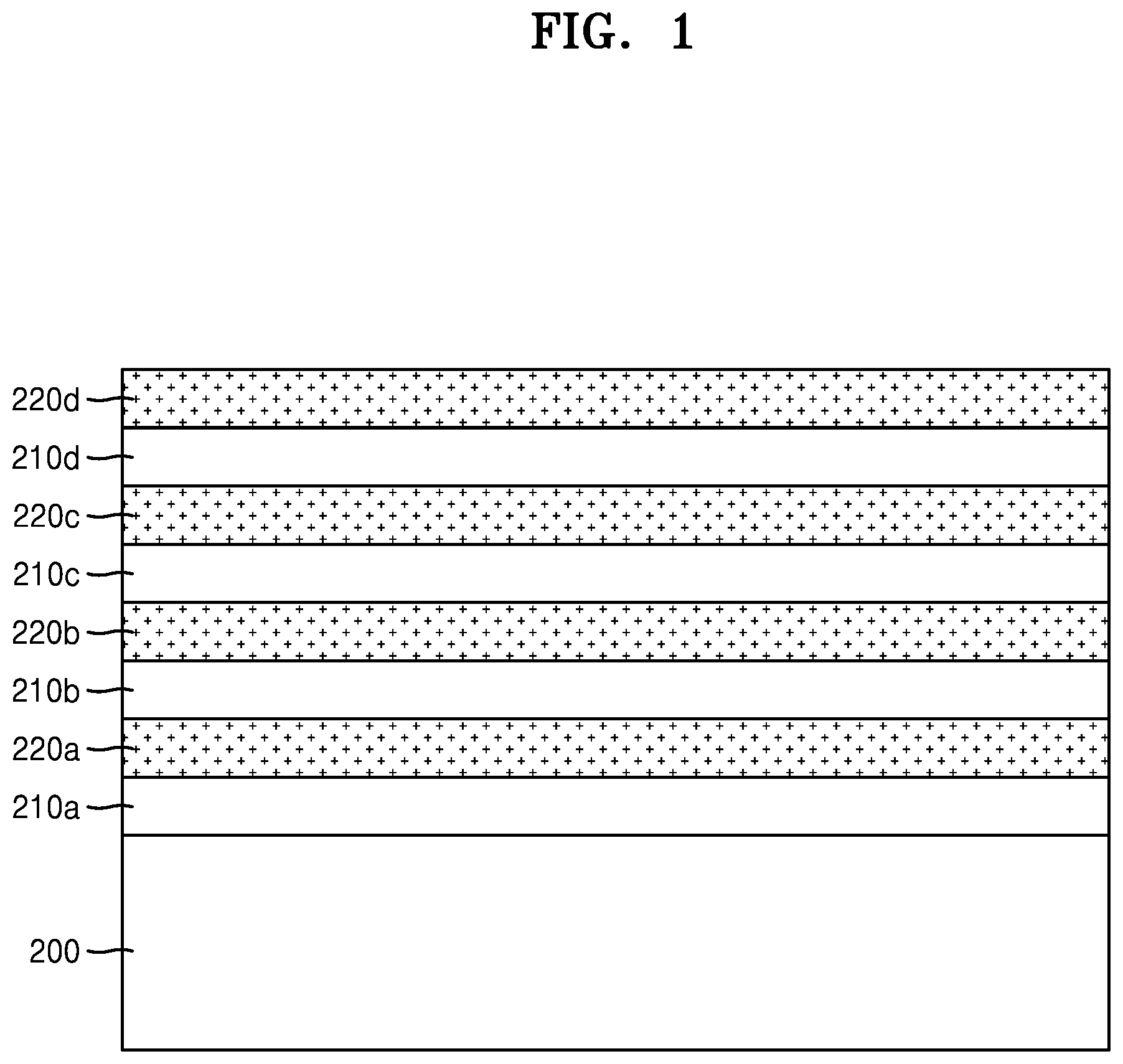
[0046] Referring to FIG. 1, a stack structure including an insulating layer 210 and a sacrificial layer 220 may be stacked on a substrate 200 a plurality of times. Although not illustrated, in some region of the stack structure, the insulating layer 210 and the sacrificial layer 220 may be etched to form channel holes, and a process may be performed to form at least some of the components of a memory cell string (MCS in FIG. 11) into the channel holes. The memory cell string may include components such as a channel, a gate conductive layer, and a gate insulating layer.
[0047] The process for forming the components of the memory cell string may be performed by directly forming at least some of a channel, a gate conductive layer, and a gate insulating layer, or may be performed by forming a sacrificial layer into a channel hole such that a channel, a gate conductive layer, and a gate insulating layer may be formed in a subsequent process, or may be performed by a combination thereof.
[0048] Thereafter, as illustrated in FIG. 2, the stack structure may be etched to form a stepped structure. As described above, the stepped structure may include a plurality of steps, and each step may have an upper surface, a lower surface, and a side surface connecting the upper surface and the lower surface. For example, the stepped structure may include at least one step ST, and one step ST may include an upper surface U on a sacrificial layer 220b, a lower surface L on a sacrificial layer 220a, and a side surface S connecting the upper surface U and the lower surface L.
[0049] Thereafter, a pad layer may be formed on the stepped structure. For this purpose, as illustrated in FIG. 3, a first layer 300 may be first formed on the stepped structure. Although the first layer 300 is illustrated as single layer, the first layer 300 may be formed as a plurality of layers. For example, the first layer 300 may be formed of the same material as the sacrificial layer 220.
[0050] The first layer 300 may be formed, for example, by atomic layer deposition, more particularly through a plasma-enhanced atomic layer deposition (PEALD) process. In an example embodiment, the PEALD process may be performed while maintaining a high plasma density condition for the first layer 300. For example, an atomic layer deposition process for the first layer 300 may be performed by applying high plasma power (i.e., introducing plasma having a high level of energy). These conditions (e.g., the high plasma density condition and the high plasma power) may result in film destruction by ions. Thus, at least a portion of the first layer 300 may be relatively weakened due to plasma application.
[0051] More particularly, a bonding structure of an upper portion of the first layer 300 may be destroyed due to plasma application. For example, as illustrated in FIG. 4, the first layer 300 may include a surface region D and an inner region C under the surface region D, and the surface region D of the first layer 300 may be weakened due to the plasma application. Thus, a transition region (see "d" in FIG. 13B) in the surface region D may be removed or minimized.
[0052] For example, when the inner region C of the first layer 300 has a first etch rate, an etch rate of the surface region D of the first layer 300 after the weakening may be substantially the same as the first etch rate. That is, the surface region D may have the same etch rate as the inner region C, except for the transition region.
[0053] In an alternative embodiment, the surface region D of the first layer 300 may have a second etch rate higher than the first etch rate. That is, the surface region D may have a higher etch rate than the inner region C, except for the transition region. A change in the physical properties of the surface region D and the inner region C of the first layer 300 through the weakening operation (e.g., a change in the wet etch rate (WER) during the subsequent etching) is illustrated in FIG. 4.
[0054] The plasma may be applied during the atomic layer deposition process or may be applied through the plasma post-treatment operation after the deposition. That is, i) the plasma may be applied during the forming of the first layer 300, ii) the plasma may be applied after the forming of the first layer 300, or iii) the plasma may be applied during and after the forming of the first layer 300. For example, FIG. 3 illustrates a state where the plasma is not applied during the forming of the first layer 300, and FIG. 4 illustrates a state in which at least a portion of the first layer 300 is weakened through the plasma application after the forming of the first layer 300.
[0055] In an alternative embodiment, the plasma application to the first layer 300 may be achieved through isotropic plasma. For example, the plasma application frequency may be a high frequency of 60 MHz or more. In this case, the directionality of the plasma may be offset due to the reduction of ion bombardment, and thus the isotropy of plasma damage to a thin film may be achieved.
[0056] The above plasma application may be referred to as an operation of weakening at least a portion of the first layer 300. Although the present embodiment has been described based on the plasma application, the present disclosure is not limited thereto. That is, an operation of weakening the first layer 300 may be performed by applying energy (e.g., thermal energy or ultraviolet (UV)) above a threshold inducing the destruction of a bonding structure of at least a portion of the first layer 300) onto the first layer 300.
[0057] Thereafter, a second layer 310 may be formed on the first layer 300 (the first layer 300 and the second layer 310 may be included in a pad layer, and the first and second layers 300 and 310 may also be referred to as a pad layer). The pad layer may be formed before an operation of forming a conductive word line structure.
[0058] For this purpose, as illustrated in FIG. 4, a second layer 310 may be formed on the sacrificial layer 220 and the first layer 300. Although the second layer 310 is illustrated as one layer, the second layer 310 may be formed as a plurality of layers. For example, the second layer 310 may be formed of the same material as the sacrificial layer 220.
[0059] The second layer 310 may be formed through an atomic layer deposition process according to the embodiments described above. In an example embodiment, a PEALD process may be performed while maintaining a low plasma density condition for the second layer 310. For example, an atomic layer deposition process for the second layer 310 may be performed by applying low plasma power. These conditions (e.g., the low plasma density condition and the low plasma power) may result in film densification by ions. Thus, the upper surface of the second layer 310 may be relatively densified due to the plasma application, and the second layer 310 may be selectively removed during the subsequent isotropic etching process (i.e., a sidewall portion of the second layer 310 may be removed preferentially).
[0060] The plasma may be applied during the atomic layer deposition process or may be applied through the plasma post-treatment operation. That is, the plasma may be applied during the forming of the second layer 310, the plasma may be applied after the forming of the second layer 310, or the plasma may be applied during and after the forming of the second layer 310.
[0061] In an example embodiment, the plasma application may be performed by using an inert gas such as argon and/or a gas including the component of the sacrificial layer 220 (e.g., nitrogen when the second layer 310 is a silicon nitride layer). A densification operation through the plasma application may be performed by applying directional plasma. Due to the directionality of plasma ions, only a portion of the second layer 310 formed on the upper surface U and the lower surface L of the step may be densified. Thus, the selective etching of the second layer 310 on the stepped structure may be achieved during the subsequent isotropic etching.
[0062] By this densification of the second layer 310, the second layer 310 may have an etch rate lower than the etch rate of the first layer 300. For example, as described above, by the weakening of the first layer 300, when the inner region C of the first layer 300 has a first etch rate and the surface region D of the first layer 300 has a second etch rate higher than the first etch rate, a third etch rate of the second layer 310 may be lower than the first etch rate and the second etch rate. In an alternative embodiment, the second etch rate of the surface region D may be higher than the first etch rate and the third etch rate (see FIG. 14).
[0063] The energy application for the densification of the second layer 310 described above may be opposite to the energy application for the weakening of the first layer 300. In other words, when energy application for destruction of a bonding structure of the first layer 300 is energy application above a threshold, energy application for strengthening a bonding structure of the second layer 310 may be energy application below the threshold.
[0064] While energy below a threshold is applied onto the second layer 310 for densification of the second layer 310, the energy below the threshold may also be applied onto the first layer 300. That is, during the densification of the second layer 310, the energy below the threshold may be applied to the first layer 300 as well as the second layer 310, and consequently an upper portion of the first layer 300 (e.g., the surface region D) and the second layer 310 may be densified.
[0065] The densification of the upper portion of the first layer may adversely affect the subsequent isotropic etching process. However, according to embodiments of the present disclosure, the weakening of at least a portion of the underlying first layer may be performed before the forming of the overlying second layer. Thus, even when the bonding of the components of at least a portion of the underlying first layer is strengthened during the forming of the overlying second layer, the strengthening of the bonding of the components of the underlying first layer may be offset by the weakening (bonding structure destruction) of the first layer described above. More particular details thereof will be described below.
[0066] Thereafter, referring to FIG. 5, an isotropic etching process may be performed on the first and second layers (300 and 310 in FIG. 4). As described above, the upper surface of the second layer 310 may be densified through plasma application under particular conditions, and the etch rate of the side surface of the second layer 310 may be higher than the etch rate of the upper/lower surface of the second layer 310. As a result, even when the isotropic etching process is performed, the second layer 310 formed on the upper surface of the stepped structure may remain. As a result, during the isotropic etching process on the second layer 310, the portion of the second layer 310 on the upper and lower surfaces of the stepped structure may remain and the portion of the second layer 310 on the side surface of the stepped structure may be removed.
[0067] A side portion of the second layer 310 may be removed to expose the first layer 300, and thus the first layer 300 may be removed by isotropic etching. As described above, since the first layer 300 has been weakened, the first layer 300 may be removed more rapidly than the second layer 310 that has been densified. As a result, during the isotropic etching process, the first layer 300 and the second layer 310 formed on the upper surface and the first layer 300 and the second layer 310 formed on the lower surface may be separated.
[0068] This may have an advantage over a related-art process of forming the first layer 300 and then forming the second layer 310 without performing the weakening. Since a densification process is performed on the second layer 310 and the first layer 300 is also densified together thereby, the etch rate of the first layer 300 may decrease, which may adversely affect the removal of the side portions of the first layer 300 and the second layer 310 in the subsequent isotropic etching process. However, according to the present disclosure, the weakening of the first layer 300 may be performed to offset the densification of the first layer 300 that may be performed during the densification of the second layer 310. Even when the bonding of the components of at least a portion of the first layer 300 is strengthened by the second densification, since the bonding structure of the first layer 300 is already weakened by the weakening of the first layer 300 in the previous operation, the subsequent isotropic etching may be performed while the etching rate of the first layer 300 is maintained to be higher than the etching rate of the second layer 310.
[0069] In some embodiments, high-density plasma may be applied during the forming of the first layer 300, and low-density plasma may be applied during the forming of the second layer 310. Thus, the plasma density supplied during the forming of the first layer 300 may be higher than the plasma density supplied during the forming of the second layer 310. In other embodiments, plasma using a hydrogen-containing material may be applied during the forming of the first layer 300, and plasma using a hydrogen-free material (or a less hydrogen-containing material) may be applied during the forming of the second layer 310. Thus, the hydrogen-containing ratio of the plasma supplied during the forming of the first layer 300 may be higher than the hydrogen-containing ratio of the plasma supplied during the forming of the second layer 310.
[0070] Thereafter, as illustrated in FIG. 6, an interlayer insulating layer 250 may be formed on the structure after the isotropic etching. The interlayer insulating layer 250 may be formed of the same material as the insulating layer 210 located between the sacrificial layers 220 of the stepped structure. For example, the sacrificial layer 220 of the stepped structure may be a silicon nitride layer, the insulating layer 210 of the stepped structure may be a silicon oxide layer, and the interlayer insulating layer 250 may be a silicon oxide layer.
[0071] Thereafter, on the upper surface of the interlayer insulating layer 250, via contacts 260 connected to at least a portion of the sacrificial layer 220 may be formed through patterning. In an alternative embodiment, the via contacts 260 may be formed after the sacrificial layer 220 is etched to form a conductive word line structure.
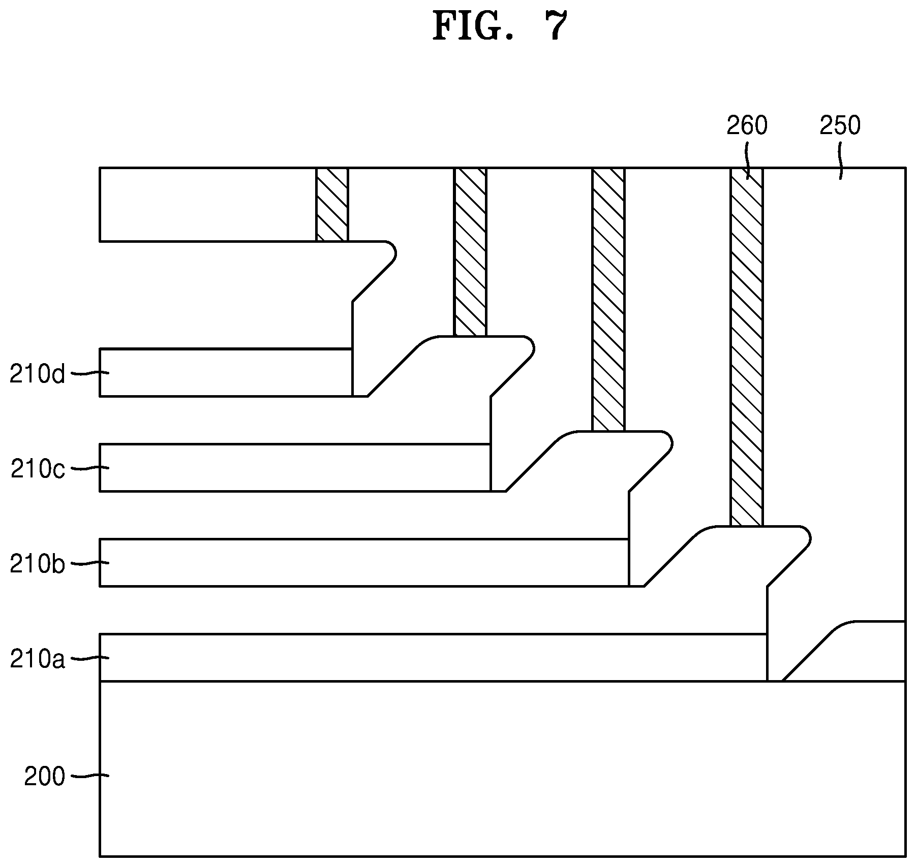
[0072] Thereafter, an operation of forming a conductive word line structure may be performed. Referring to FIG. 7, an operation of removing the sacrificial layer (220 in FIG. 6) and the pad layers (300 and 310 in FIG. 6) may be performed. For example, the sacrificial layer and the pad layers may be etched to expose a channel (not illustrated), the insulating layer 210, the interlayer insulating layer 250, and the via contacts 260. Accordingly, the sacrificial word line structure including the sacrificial layer (220 in FIG. 6) and the pad layers (300 and 310 in FIG. 6) may be removed. In an alternative embodiment, during the etching of the sacrificial layer and the pad layers, pad layers (300' and 310' in FIG. 6) formed on the substrate 200 may also be simultaneously removed, and thus a portion of the upper surface of the substrate 200 may be exposed.
[0073] Referring to FIG. 8, a conductive word line structure WL may be formed through the exposed space. The conductive word line structure WL may be formed to correspond to a space from which the sacrificial word line structure is removed. That is, a conductive word line structure may be formed by filling a conductive material in the space from which the sacrificial layer and the pad layers are removed.
[0074] The formed conductive word line structure WL may include a conductive layer C0 extending toward the channel, a first conductive layer C1 and a second conductive layer C2 on the conductive layer C0. In other words, the conductive word line structure WL may include a word line conductive layer C0 corresponding to the sacrificial layer (220 in FIG. 6), a first conductive layer C1 corresponding to the first layer (300 in FIG. 6), and a second conductive layer C2 corresponding to the second layer (310 in FIG. 6).
[0075] As described above, since the first layer 300 is weakened and the second layer 310 is densified, the second layer 310 may be less removed during the isotropic etching in comparison with the first layer 300. As a result, the second conductive layer C2 corresponding to the second layer 310 may protrude in comparison with the first conductive layer C1 corresponding to the first layer 300. Although FIG. 8 illustrates that the second conductive layer C2 protrudes at one side portion in comparison with the first conductive layer C1, this is merely an example and the second conductive layer C2 may protrude at both end portions in comparison with the first conductive layer C1.
[0076] The substrate processing method according to the embodiments of the present disclosure may be summarized as follows. [0077] Operation 1: stacking, a plurality of times, a stack structure including an insulating layer and a first sacrificial layer (see FIG. 1). [0078] Operation 2: forming a stepped structure by etching the stack structure (see FIG. 2). [0079] Operation 3: forming a second sacrificial layer (first layer 300) on the first sacrificial layer and weakening at least a portion of the second sacrificial layer (see FIG. 3). The weakening may be performed after the forming of the second sacrificial layer, or may be performed by adjusting process parameters in the forming of the second sacrificial layer. [0080] Operation 4: forming a third sacrificial layer (second layer 310) on the second sacrificial layer (see FIG. 4). [0081] Operation 5: etching (e.g., isotropic-etching or wet-etching) at least a portion of a sacrificial word line structure including the first sacrificial layer, the second sacrificial layer, and the third sacrificial layer (see FIG. 5). [0082] Operation 6: forming an interlayer insulating layer on the sacrificial word line structure and forming a via contact (see FIG. 6). The forming of the via contact may be performed after the forming of the word line. [0083] Operation 7: removing the sacrificial word line structure (see FIG. 7). [0084] Operation 8: forming a conductive word line structure corresponding to the sacrificial word line structure (see FIG. 8).
[0085] As such, according to the present disclosure, the densification of the first layer that may occur during formation of the second layer that corresponds to an upper portion of a pad layer (or that may be performed after formation of the second layer) may be offset by previously destroying the bonding structure of at least a portion (e.g., an upper surface region) of the first layer that corresponds to a lower portion of the pad layer. That is, the first layer may be smoothly removed during the subsequent isotropic etching, by preventing, through the pre-performed weakening of the first layer, the densification of the underlying first layer that may occur while the portions on the upper and lower surfaces of the second layer are densified by a selective plasma process on the second layer on the first layer. As a result, the first and second layers may be completely separated between the top and bottom portions of the stepped structure, thereby preventing the short circuit between the word lines.
[0086] As described above, according to the embodiments of the present disclosure, energy application above a certain threshold may be performed during the weakening of the first layer 300 including a surface region D and an inner region C under the surface region D. Accordingly, the inner region C may have a first etch rate, the surface region D may have a second etch rate, and the second etch rate may be higher than the first etch rate due to a weakened state of the surface region D coming from the destruction of bonding structure.
[0087] Thereafter, the second layer 310 may be densified, and thus surface region D of the first layer 300 may also be densified together. In this case, the second etch rate may be reduced back by the densification of the surface region D. As a result, the second etch rate of the surface region D may be substantially equal to the first etch rate of the inner region C.
[0088] In an alternative embodiment, the second etch rate of the surface region D may be maintained to be higher than the first etch rate of the inner region C, despite the densification of the surface region D of the first layer 300 that may occur during the densification of the second layer 310. More particularly, the second etch rate of the surface region D may be adjusted by adjusting the energy applied during the weakening of the first layer 300. For example, a significant amount of energy may be applied during the weakening of the first layer 300 to significantly increase the second etch rate of the surface region D, and thus the second etch rate of the surface region D may still be maintained to be higher than the first etch rate of the inner region C, despite the densification of the second layer 310. In other words, the second etch rate of the surface region D may be adjusted (e.g., increased) by adjusting (e.g., significantly increasing) the energy applied during the weakening of the first layer 300.
[0089] In an additional embodiment, the second etch rate of the surface region D may be adjusted (e.g., increased) by adjusting (e.g., reducing) the energy applied during the densification of the second layer 310. In other words, the second etch rate may be substantially increased by reducing the densification of the surface region D.
[0090] FIGS. 9 and 10 illustrate a substrate processing method according to embodiments of the present disclosure. The substrate processing method according to these embodiments may be a modification of the substrate processing method according to the above embodiments. Hereinafter, redundant descriptions between the embodiments will be omitted for conciseness.
[0091] Referring to FIG. 9, by increasing the energy applied during the weakening of the first layer 300, or by reducing the energy applied during the densification of the second layer 310, an isotropic etching process may be performed after the second etch rate of the surface region D is increased. In this case, the second etch rate of the surface region D may still be higher than the first etch rate of the inner region C and the third etch rate of the second layer 310, and consequently the deepest recess may be formed in the surface region D during the isotropic etching.
[0092] For example, after the isotropic etching, in the first layer 300, an upper recess R1 may be formed in the surface region D, and a lower recess R2 may be formed in the inner region C. In this case, the extension length of the upper recess R1 (i.e., the depth of the recess in the lateral direction) may be greater than the extension length of the lower recess R2. Meanwhile, a recess may be formed in the sidewall of the second layer 310. Since the second layer 310 is in a densified state, the extension length of the recess formed in the second layer 310 may be smaller than the extension length of the upper recess R1 and may be smaller than the extension length of the lower recess R2.
[0093] FIG. 10 illustrates a conductive word line structure formed based on the first layer 300 and the second layer 310. Referring to FIG. 10, a conductive word line structure WL may include a word line conductive layer C0 corresponding to the sacrificial layer (220 in FIG. 6), a first conductive layer C1 corresponding to the first layer (300 in FIG. 6), and a second conductive layer C2 corresponding to the second layer (310 in FIG. 6).
[0094] The first conductive layer C1 may include a surface region D' and an inner region C' under the surface region D'. In this case, the first conductive layer C1 may include an upper recess R1' in the surface region D' and a lower recess R2' in the inner region C'. The extension length of the upper recess R1' may be greater than the extension length of the lower recess R2'. Also, a recess may be formed in the sidewall of the second conductive layer C2. In this case, the extension length of the recess formed in the second conductive layer C2 may be smaller than the extension length of the upper recess R1' and may be smaller than the extension length of the lower recess R2'.
[0095] FIG. 11 is a circuit diagram of a semiconductor device according to an embodiment of the present disclosure. The semiconductor device may be formed by the substrate processing method according to the above embodiments. Hereinafter, redundant descriptions between the embodiments will be omitted for conciseness.
[0096] Referring to FIG. 11, a semiconductor memory device may include a substrate 200, a memory cell string MCS, a first word line WL1, and a second word line WL2.
[0097] The memory cell string MCS may have a structure protruding and extending on the substrate 200. The memory cell string MCS may include a plurality of memory cells. Although only four memory cells are illustrated in FIG. 11, one memory cell string MCS may include fewer or more memory cells as necessary.
[0098] The first word line WL1 may be connected to the first memory cell MC1. For example, the first word line WL1 may be formed to extend toward the channel of the first memory cell MC1. Likewise, the second word line WL2 may be connected to the second memory cell MC2 and may be formed to extend toward the channel of the second memory cell MC2.
[0099] At least two of the first word line WL1 and the second word line WL2 may include the word line structure formed through the operations illustrated in FIGS. 2 to 10. Thus, at least one of the first word line WL1 and the second word line WL2 may include a word line conductive layer C0 extending toward the channel, a first conductive layer C1 on the word line conductive layer C0, and a second conductive layer C2 on the first conductive layer C1.
[0100] As described above, each of the word line conductive layer C0, the first conductive layer C1, and the second conductive layer C2 may include a recess on the side portion. The width of the recess of the first conductive layer C1 may be larger than the width of the recess of the word line conductive layer C0. Also, the width of the recess of the first conductive layer C1 may be larger than the width of the recess of the second conductive layer C2.
[0101] More particularly, the first conductive layer C1 may include a surface region D and an inner region C under the surface region D. In this case, the first conductive layer may include an upper recess R1' in the surface region D and a lower recess R2' in the inner region C, and the width of the upper recess R1' (i.e., the extension length in the horizontal direction) may be larger than the width of the lower recess R2' (i.e., the extension length in the horizontal direction).
[0102] The shape of the recess of the first conductive layer, particularly, the shapes of the upper recess R1' and the lower recess R2', may be formed as a result of the above substrate processing method. That is, the shape of the recess of the first conductive layer, particularly, the shapes of the upper recess R1' and the lower recess R2' of the first conductive layer may be formed by weakening the first layer and/or by densifying the second layer (and by adjusting the process parameters thereof).
[0103] Although the structural features related to the word line have been described in the embodiment of FIGS. 10 and 11, the present disclosure is not limited thereto. The semiconductor device in the embodiments of the present disclosure described in FIGS. 10 and 11 may include any or all of the features according to the above method, and these may be included without mutual contradiction.
[0104] FIG. 12 illustrates a substrate processing method according to embodiments of the present disclosure. The substrate processing method according to these embodiments may be a modification of the substrate processing method according to the above embodiments. Hereinafter, redundant descriptions between the embodiments will be omitted for conciseness.
[0105] Referring to FIG. 12A, a gate stack may be formed, and then a stepped (staircase) structure may be formed. For example, the gate stack may be formed by alternately stacking SiO and SiN films. The stepped structure may be formed through a slimming process on the stack structure. Subsequently, a second SiN film may be formed on the stepped structure. The second SiN film may be formed by PEALD, a dichlorosilane (DCS) or aminosilane source may be used as a silicon (Si) source, and NH.sub.3 may be used as a nitrogen (N) source. NH.sub.3 may be activated by plasma and react with the Si source. As a result, a SiN film may be formed on the upper surface, the side surface, and the lower surface of the stepped structure.
[0106] Thereafter, referring to FIG. 12B, plasma processing may be performed on the second SiN film. By performing the plasma processing, the bonding structure of the surface of the second SiN film may be destroyed. For this purpose, plasma power above a critical point (or threshold) may be applied. As a result, thin film bonding structure destruction may occur rather than the densification of the thin film by ion bombardment.
[0107] Thereafter, referring to FIG. 12C, in this operation, a third SiN film may be formed on the second SiN film by PEALD. A DCS or aminosilane-based Si source may be used as a silicon source, and NH.sub.3 or N2 may be used as an N source. NH.sub.3 may be activated by plasma and react with the Si source to form the third SiN film on the substrate. However, the WER of the third SiN film may be set to be lower than the WER of the second SiN film. Since the WER increases as the hydrogen content in the film increases, the amount of NH.sub.3 supplied may be smaller than that in the forming of the second SiN film. For example, the NH.sub.3 flow rate may be reduced or the NH.sub.3 supply time may be reduced in comparison with the operation (b). In another example, a third SiN film having a lower WER than the second SiN film using NH.sub.3 may be formed by forming a third SiN film by using a hydrogen-free N2 gas.
[0108] As described above, when the third SiN film is formed, the WER of the surface region (upper region) of the underlying second SiN film may become lower than the WER of the inner region (lower region) of the second SiN film due to the influence of plasma exerted during forming the third SiN film. Thus, the surface portion of the second SiN film may be plasma-processed before the forming of the third SiN film to weaken the bonding structure of the surface portion of the second SiN film. Thereafter, when the third SiN film is formed, the WER of the surface portion of the second SiN film may maintain the original (intended) WER of the second SiN film.
[0109] Referring to FIG. 12D, selective etching may be performed to remove the SiN film deposited on the side surface of the step. On the other hand, the SiN film formed on the upper surface and the lower surface may remain to form a landing pad to be connected to a via hole metal film formed in a subsequent process. The selective etching may be caused by the linearity of the radical supplied during the forming of the second SiN film and the third SiN film. That is, the SiN film deposited on the upper and lower surfaces of the stepped structure, which is perpendicular to the propagation direction of the radical, may be more hardened by the ion bombardment of the radical than the SiN film deposited on the side surface of the stepped structure, which is parallel to the propagation direction of the radical. Thus, in a subsequent wet etching process, the side SiN film may be etched first.
[0110] As such, the etch selectivity in the wet etching illustrated in FIG. 12D may be improved by introducing SiN compound films having different WERs. That is, the etching of the SiN films of the upper and lower surfaces during the wet etching may be minimized due to the third SiN film having a low WER. That is, the third SiN film may function as a protective film for the underlying SiN film.
[0111] The inventor of the present disclosure has found that there is a factor that hinders the etch selectivity of the dual SiN film (double SiN layer). More particularly, it is found that the WER of the portion of the second SiN film in the boundary layer with the third SiN film is lower than the WER of the other portion of the second SiN film due to the influence of plasma exerted during forming the third SiN film. Thus, when the second SiN film formed on the side surface of the step is wet-etched, a residual SiN film may remain on the step, which may be an obstacle to the improvement of the etch selectivity. Also, it is found that a short circuit occurs when the SiN films on the upper and lower surfaces are connected and are replaced with a metal in the subsequent process due to the second SiN film remaining on the side surface.
[0112] According to the technical idea of the present disclosure, the above-mentioned problems may be solved. That is, as described in FIG. 12B, a bonding structure of the second SiN film near the upper surface of the second SiN film may be weakened by the plasma treatment, and thus the transition region of the WER on the surface of the second SiN film may be minimized even when the third SiN film is subsequently formed. FIG. 13 illustrates the difference in WER with respect to each portion according to the presence or absence of the operation (b).
[0113] Referring to FIG. 13A, a region (a) of the second SiN film may be divided into an inner region C and a surface region D including a transition region (d). A region (b) of the third SiN film may contact the transition region (d) of the second SiN film, and the transition region (d) may be a boundary region between the third SiN film and the second SiN film. The boundary region may correspond to a portion of the second SiN film, particularly, the surface of the second SiN film contacting the third SiN film.
[0114] As described above, the third SiN film may have a lower WER than the second SiN film. That is, the third SiN film may be a dense film and may be achieved by suitably adjusting the plasma conditions, for example, by using a nitrogen reaction gas with low hydrogen content or by reducing the ammonia supply. However, when the third SiN film is deposited on the second SiN film, the surface of the second SiN film may be influenced by the plasma for forming the third SiN film, which is denser than the second SiN film, to have a low WER than the film quality required for the second SiN film. That is, as illustrated in FIG. 13A, a WER transition region (d) may be formed on the surface of the second SiN film.
[0115] The transition region (d) may make it difficult to remove the second SiN film on the side surface of the step. That is, due to the different wet etch conditions, a separate etching process should be added, thus increasing the production time and cost and the difficulties of the process. Also, due to the SiN film remaining on the side surface of the step, the etch selectivity of the SiN film between the upper surface (lower surface) and the side surface may be degraded. Also, there may be an imbalance in that the SiN film remains on one side surface of the step but does not remain on another side surface of the step.
[0116] Also, when the number of steps increases, the forming of a low-thickness SiN film may be required and thus the wet etching time margin (i.e., reducing the wet-etchable time) may be reduced, thus increasing the possibility of the side-surface SiN film remaining without being sufficiently removed due to the transition region (d). The remaining SiN film may connect the SiN films of the upper and lower surfaces of the step in the subsequent metal filling process (the landing pad; filled with a metal in the subsequent process), which may result in a short-circuit problem of the semiconductor device.
[0117] In FIG. 13B, the second SiN film (i.e., the underlying SiN film) may be weakened. More particularly, after the second SiN film is deposited, the surface of the second SiN film may be plasma-treated to destroy the bonding structure of the surface of the second SiN film and to induce a less dense film. For this purpose, by applying the plasma power above a certain critical point, the surface bonding of the thin film may be destroyed rather than the densification of the thin film. Thereafter, when the third SiN film is deposited, even though the surface of the second SiN film is influenced by the plasma for depositing the third SiN film, since the surface of the second SiN film is softened beforehand, the generation of the WER transition region (d) in the surface region D of the second SiN film due to the plasma during the forming of the third SiN film may be suppressed or minimized.
[0118] FIG. 14 is a modification of the embodiment of FIG. 13, in which more enhanced weakening is applied to the second SiN film (i.e., the underlying SiN film). More particularly, after the deposition of the second SiN film, by much stronger plasma-treatment on the surface of the second SiN film than in the example of FIG. 13, even after the deposition of the third SiN film, the WER of most of the surface region D of the second SiN film may be higher than the WER of the underlying inner region C and the generation of the WER transition region (d) may also be suppressed. As a result, the portion of the surface region D of the second SiN film may be etched more easily, and consequently, it may be possible to smoothly cope with the reduced wet etching time margin.
[0119] FIG. 15 illustrates the side/top wet etch selectivity of layers according to whether plasma treatment is applied to the second SiN film. Subsequent wet etching was performed by using dHF under the condition of 100:1. According to the experimental data, a selectivity improvement of up to 30% may be achieved when the plasma treatment is performed. Particularly, in the case of performing the plasma treatment, the etch selectivity may be improved when a material including nitrogen is applied (i.e., when a material corresponding to the components of the thin film is supplied).
[0120] As such, according to the embodiments of the present disclosure, the first SiN film may be formed by PEALD in a stepped gate stack structure, and then the surface of the first SiN film may be softened through plasma treatment. Thereafter, the second SiN film may be formed by PEALD under a plasma condition for forming a film denser than the first SiN film. The formation of the WER transition region in the boundary layer between the first SiN film and the second SiN film may be suppressed by softening in advance the surface of the first SiN film through the plasma treatment, and consequently, the wet etch selectivity in the stepped structure may be improved.
[0121] It is to be understood that the shape of each portion in the accompanying drawings is illustrative for a clear understanding of the present disclosure. It should be noted that the present disclosure may be modified into various shapes other than the illustrated shapes. Like reference numerals in the drawings may refer to like elements.
[0122] It will be apparent to those of ordinary skill in the art that the present disclosure is not limited to the above embodiments and the accompanying drawings and various substitutions, modifications, and alterations may be made therein without departing from the spirit and scope of the present disclosure.
[0123] It should be understood that embodiments described herein should be considered in a descriptive sense only and not for purposes of limitation. Descriptions of features or aspects within each embodiment should typically be considered as available for other similar features or aspects in other embodiments.
[0124] While one or more embodiments have been described with reference to the figures, it will be understood by those of ordinary skill in the art that various changes in form and details may be made therein without departing from the spirit and scope of the disclosure as defined by the following claims.
* * * * *
D00000
D00001
D00002
D00003
D00004
D00005
D00006
D00007
D00008
D00009
D00010
D00011
D00012

D00013

D00014

XML
uspto.report is an independent third-party trademark research tool that is not affiliated, endorsed, or sponsored by the United States Patent and Trademark Office (USPTO) or any other governmental organization. The information provided by uspto.report is based on publicly available data at the time of writing and is intended for informational purposes only.
While we strive to provide accurate and up-to-date information, we do not guarantee the accuracy, completeness, reliability, or suitability of the information displayed on this site. The use of this site is at your own risk. Any reliance you place on such information is therefore strictly at your own risk.
All official trademark data, including owner information, should be verified by visiting the official USPTO website at www.uspto.gov. This site is not intended to replace professional legal advice and should not be used as a substitute for consulting with a legal professional who is knowledgeable about trademark law.