Surface Roughening Of Cmc And Coated Cmc
Van der Laag; Niels ; et al.
U.S. patent application number 16/348519 was filed with the patent office on 2019-11-28 for surface roughening of cmc and coated cmc. The applicant listed for this patent is Siemens Aktiengesellschaft. Invention is credited to Arturo Flores Renteria, David J. Mitchell, Niels Van der Laag.
| Application Number | 20190359532 16/348519 |
| Document ID | / |
| Family ID | 57406044 |
| Filed Date | 2019-11-28 |

| United States Patent Application | 20190359532 |
| Kind Code | A1 |
| Van der Laag; Niels ; et al. | November 28, 2019 |
SURFACE ROUGHENING OF CMC AND COATED CMC
Abstract
By surface roughening of CMC component via a pico-laser treatment a good adhering of a plasma sprayed coating is achieved.
| Inventors: | Van der Laag; Niels; (Vaterstetten, DE) ; Flores Renteria; Arturo; (Berlin, DE) ; Mitchell; David J.; (Oviedo, FL) | ||||||||||
| Applicant: |
|
||||||||||
|---|---|---|---|---|---|---|---|---|---|---|---|
| Family ID: | 57406044 | ||||||||||
| Appl. No.: | 16/348519 | ||||||||||
| Filed: | November 7, 2017 | ||||||||||
| PCT Filed: | November 7, 2017 | ||||||||||
| PCT NO: | PCT/EP2017/078459 | ||||||||||
| 371 Date: | May 9, 2019 |
| Current U.S. Class: | 1/1 |
| Current CPC Class: | B23K 2103/52 20180801; C04B 41/5346 20130101; C04B 41/5031 20130101; B23K 2103/16 20180801; B23K 26/0624 20151001; B23K 26/3584 20180801; C04B 41/5042 20130101; C04B 41/91 20130101; C04B 41/0036 20130101; C04B 41/009 20130101; C04B 41/87 20130101 |
| International Class: | C04B 41/00 20060101 C04B041/00; B23K 26/0622 20060101 B23K026/0622; B23K 26/352 20060101 B23K026/352; C04B 41/53 20060101 C04B041/53; C04B 41/91 20060101 C04B041/91; C04B 41/50 20060101 C04B041/50; C04B 41/87 20060101 C04B041/87 |
Foreign Application Data
| Date | Code | Application Number |
|---|---|---|
| Nov 14, 2016 | EP | 16198638.5 |
Claims
1. A method of roughening a surface of a CMC substrate of a CMC component, wherein a pico-laser with pulses in the pico-second area is used to roughen or engrave the surface of the CMC substrate.
2. The method according to claim 1, wherein holes, including at least one of round holes, engravings, and grids are produced into the surface of the CMC substrate.
3. A product, produced by a method according to claim 1, which has a ceramic layer on a roughened surface of a substrate, wherein the ceramic layer has a APS applied-like microstructure.
4. The product according to claim 3, wherein the material of the ceramic layer comprises zirconia, 8YSZ, alumina, 48YSZ or a 48YSZ-alumina mixture.
5. The product according to claim 3, wherein the surface of the substrate under the ceramic layer comprises holes, especially including at least one of round holes, elongated engravings, and grids.
6. The product according to claim 5, wherein the depth of the holes 10, engravings or grids are between 50 .mu.m to 100 .mu.m.
Description
CROSS-REFERENCE TO RELATED APPLICATIONS
[0001] This application claims priority to PCT Application No. PCT/EP2017/078459, having a filing date of Nov. 7, 2017, which is based on European Application No. 16198638.5, having a filing date of Nov. 14, 2016, the entire contents both of which are hereby incorporated by reference.
FIELD OF TECHNOLOGY
[0002] The following relates to a surface roughening of a CMC part which will be coated with a ceramic layer.
BACKGROUND
[0003] Oxide based Ceramic Matrix Composites (CMC's) provide a higher temperature capability (1423K) than superalloys 1273K C) and superior oxidation resistance. The limited fracture resistance and damage tolerance of ceramic materials is substantially improved by the fiber reinforcement. However, the load bearing capacity (mechanical strength) of these Oxide-Oxide (Ox-Ox) CMCs is also limited by grain growth and reaction processes with the matrix and/or the environment at 1423K and higher. With firing temperatures as high as 1873 1973K, Ox-Ox CMCs need Environmental Barrier Coatings (EBCs) that maintain CMCs below 1423K. Thus, CMCs can be used to its full potential, only if the coating can be integrated in to the system design.
[0004] For oxide-oxide CMCs, application of the thermal barrier was by an FGI (Friable Graded Insulation) system. FGI was coprocessed along with CMC, however, currently the hollow spheres needed for this coating system are not commercially available. In addition, the capability of the coating to recession at high surface temperatures (1873K-1973K) is not expected to match behavior of zirconia-based materials.
SUMMARY
[0005] The current proposal takes into account the experience of using proper roughening of the substrate surface for TBC adhesion.
[0006] The description and the figure are only examples of embodiments of the invention.
[0007] Application of plasma sprayed coating on CMC surface is not easy. Depending upon the local macro roughness of the ceramic fibers and matrix infiltration characteristics, the adhesion of plasma sprayed coatings are poor. Plasma sprayed coating don't adhere well to CMC surfaces especially on the surface of in-plane fibers direction.
[0008] The proposed embodiments provide significant improvements in the ability for plasma sprayed coatings to adhere to the CMC substrate.
[0009] Better adhesion is achieved by increasing mechanical interlocking via surface roughening of the CMC by using pico-laser machining. This technology allows the grinding of the CMC surface in a better controlled way compared to standard grit-blasting processing or as received conditions. Moreover, the pico-laser avoids the glassing of the ceramic material surface by its capability of almost fully evaporate the CMC during machining.
[0010] The inventive step is the use of pico-laser to prepare the CMC surface in the out of plane configuration prior to the APS coating process enhancing the engineering capability of the surface preparation compared to standard processes like grit blasting.
[0011] Furthermore, no extra phases are introduced into the top region of the CMC due to the capability of pico-laser machining to overcome glassing. This allows an improved chemical bonding with the EBC without a potentially weak glassy interlayer. Additionally, it allows an enhanced shape of the roughness (macro- and micro roughness of hills and valleys).
BRIEF DESCRIPTION
[0012] Some of the embodiments will be described in detail, with references to the following Figures, wherein like designations denote like members, wherein:
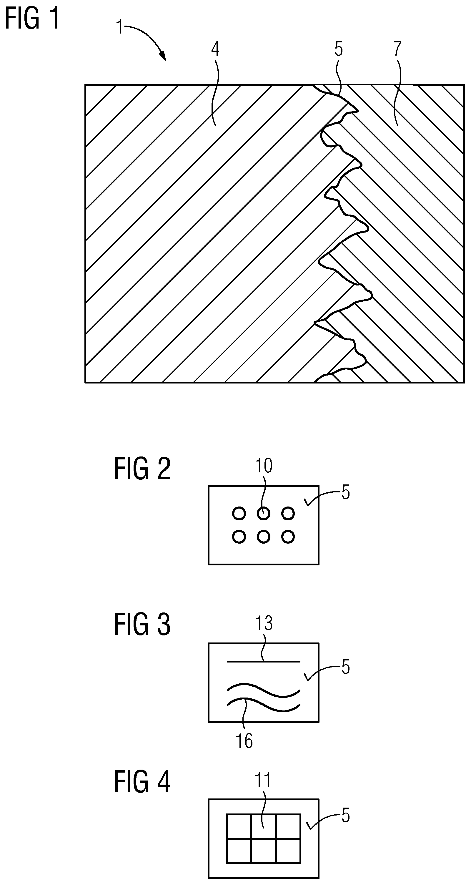
[0013] The FIG. 1 shows a CMC component 1 which comprises a CMC substrate 4 with a surface 5.
DETAILED DESCRIPTION
[0014] The substrate 4 is made of a CMC, of an Ox-Ox-CMC, but not limited.
[0015] As described above the surface 5 of the CMC-substrate 4 is roughened or structured by a pico-laser, which leads to no melting of the material of the CMC. Pulses in the pico-second region are used, especially max 900 ps.
[0016] The surface 5 of the CMC-substrate 4 can comprise holes 10 (FIG. 2), especially round holes, elongated engravings 13, 16 (FIG. 3), which can be straight 13 or waved 16 or grids 11 (FIG. 4). These forms 10, 13, 16, 11 can appear alone or in combination with each other in the surface 5.
[0017] An alternative is to randomly remove locally material from the surface to roughen the surface 5 deeper and additionally (FIG. 5).
[0018] Especially a depth of 50 .mu.m to 100 .mu.m is at least given for the holes 10, engravings 13, 16 or grids 11.
[0019] After that a ceramic layer 7 is applied on which is performed by APS.
[0020] The material of the ceramic layer 7 is zirconia (ZrO.sub.2), stabilized zirconia 8YSZ and/or an alumina sublayer, or alumina or 48YSZ (fully stabilized zirkonia).
[0021] Although the invention has been illustrated and described in greater detail with reference to the preferred exemplary embodiment, the invention is not limited to the examples disclosed, and further variations can be inferred by a person skilled in the art, without departing from the scope of protection of the invention.
[0022] For the sake of clarity, it is to be understood that the use of "a" or "an" throughout this application does not exclude a plurality, and "comprising" does not exclude other steps or elements.
* * * * *
D00000
D00001
XML
uspto.report is an independent third-party trademark research tool that is not affiliated, endorsed, or sponsored by the United States Patent and Trademark Office (USPTO) or any other governmental organization. The information provided by uspto.report is based on publicly available data at the time of writing and is intended for informational purposes only.
While we strive to provide accurate and up-to-date information, we do not guarantee the accuracy, completeness, reliability, or suitability of the information displayed on this site. The use of this site is at your own risk. Any reliance you place on such information is therefore strictly at your own risk.
All official trademark data, including owner information, should be verified by visiting the official USPTO website at www.uspto.gov. This site is not intended to replace professional legal advice and should not be used as a substitute for consulting with a legal professional who is knowledgeable about trademark law.