Wireless Power Transmitting Apparatus And Wireless Power Receiving Apparatus
LEE; Yun Bok ; et al.
U.S. patent application number 16/520111 was filed with the patent office on 2019-11-14 for wireless power transmitting apparatus and wireless power receiving apparatus. This patent application is currently assigned to LG INNOTEK CO., LTD.. The applicant listed for this patent is LG INNOTEK CO., LTD.. Invention is credited to Soon Young HYUN, Yun Bok LEE, Young Kil SONG.
| Application Number | 20190348854 16/520111 |
| Document ID | / |
| Family ID | 55630861 |
| Filed Date | 2019-11-14 |


| United States Patent Application | 20190348854 |
| Kind Code | A1 |
| LEE; Yun Bok ; et al. | November 14, 2019 |
WIRELESS POWER TRANSMITTING APPARATUS AND WIRELESS POWER RECEIVING APPARATUS
Abstract
A wireless power transmitting apparatus can include a substrate; a first transmitting coil and a second transmitting coil disposed on the substrate; a third transmitting coil disposed on the first transmitting coil and the second transmitting coil; and an adhesive disposed between the substrate and the first and the second transmitting coils, in which the substrate includes a first portion disposed inside an inner circumference of the first transmitting coil; a second portion disposed inside an inner circumference of the second transmitting coil; a third portion disposed between the first transmitting coil and the second transmitting coil; and a peripheral portion disposed outside an outer circumference of the first transmitting coil and an outer circumference of the second transmitting coil, in which an inner area disposed inside an inner circumference of the third transmitting coil overlaps the third portion, a part of the first transmitting coil and a part of the second transmitting coil in a vertical direction perpendicular to the substrate.
| Inventors: | LEE; Yun Bok; (Seoul, KR) ; SONG; Young Kil; (Seoul, KR) ; HYUN; Soon Young; (Seoul, KR) | ||||||||||
| Applicant: |
|
||||||||||
|---|---|---|---|---|---|---|---|---|---|---|---|
| Assignee: | LG INNOTEK CO., LTD. Seoul KR |
||||||||||
| Family ID: | 55630861 | ||||||||||
| Appl. No.: | 16/520111 | ||||||||||
| Filed: | July 23, 2019 |
Related U.S. Patent Documents
| Application Number | Filing Date | Patent Number | ||
|---|---|---|---|---|
| 15515022 | Mar 28, 2017 | |||
| PCT/KR2015/009462 | Sep 8, 2015 | |||
| 16520111 | ||||
| Current U.S. Class: | 1/1 |
| Current CPC Class: | H01F 27/245 20130101; H02J 50/12 20160201; H01F 27/255 20130101; H02J 50/70 20160201; H01F 1/14733 20130101; H02J 50/005 20200101; H01F 1/26 20130101; H01F 27/36 20130101; H01F 27/2871 20130101; H02J 50/50 20160201; H01F 27/2804 20130101; H01F 38/14 20130101; H01F 1/20 20130101; H02J 7/025 20130101; H01F 1/14775 20130101; H01F 1/14791 20130101 |
| International Class: | H02J 7/02 20060101 H02J007/02; H02J 50/50 20060101 H02J050/50; H01F 1/26 20060101 H01F001/26; H01F 38/14 20060101 H01F038/14; H02J 50/12 20060101 H02J050/12; H01F 27/36 20060101 H01F027/36; H01F 27/28 20060101 H01F027/28; H01F 1/147 20060101 H01F001/147; H01F 1/20 20060101 H01F001/20; H01F 27/255 20060101 H01F027/255; H01F 27/245 20060101 H01F027/245 |
Foreign Application Data
| Date | Code | Application Number |
|---|---|---|
| Sep 29, 2014 | KR | 10-2014-0130529 |
Claims
1. A wireless power transmitting apparatus, comprising: a substrate; a first transmitting coil and a second transmitting coil disposed on the substrate; a third transmitting coil disposed on the first transmitting coil and the second transmitting coil; and an adhesive disposed between the substrate and the first and the second transmitting coils, wherein the substrate comprises: a first portion disposed inside an inner circumference of the first transmitting coil; a second portion disposed inside an inner circumference of the second transmitting coil; a third portion disposed between the first transmitting coil and the second transmitting coil; and a peripheral portion disposed outside an outer circumference of the first transmitting coil and an outer circumference of the second transmitting coil, wherein an inner area disposed inside an inner circumference of the third transmitting coil overlaps the third portion, a part of the first transmitting coil and a part of the second transmitting coil in a vertical direction perpendicular to the substrate, wherein the first portion comprises a first overlapping area overlapping the third transmitting coil in the vertical direction and a first non-overlapping area not overlapping the third transmitting coil in the vertical direction, and wherein the second portion comprises a second overlapping area overlapping the third transmitting coil in the vertical direction and a second non-overlapping area not overlapping the third transmitting coil in the vertical direction.
2. The wireless power transmitting apparatus of claim 1, wherein the substrate further comprises: a guide portion disposed between the first transmitting coil and the second transmitting coil.
3. The wireless power transmitting apparatus of claim 2, further comprising: lead wires of the third transmitting coil, the lead wires being disposed in the guide portion.
4. The wireless power transmitting apparatus of claim 1, wherein the substrate further comprises: a recess on a lateral side of the substrate.
5. The wireless power transmitting apparatus of claim 4, further comprising: lead wires of the third transmitting coil; and terminals of the lead wires, wherein the terminals of the lead wires of the third transmitting coil are disposed in the recess.
6. A wireless power transmitting apparatus, comprising: a substrate; a first transmitting coil and a second transmitting coil disposed on the substrate, and a third transmitting coil disposed on the first transmitting coil and the second transmitting coil; wherein the substrate comprises: a first portion disposed inside an inner circumference of the first transmitting coil; a second portion disposed inside an inner circumference of the second transmitting coil; and a third portion disposed between the first transmitting coil and the second transmitting coil, and wherein an inner area disposed inside an inner circumference of the third transmitting coil overlaps the third portion, a part of the first transmitting coil and a part of the second transmitting coil in a vertical direction perpendicular to the substrate.
7. The wireless power transmitting apparatus of claim 6, wherein the substrate further comprises: a guide portion disposed between the first transmitting coil and the second transmitting coil.
8. The wireless power transmitting apparatus of claim 7, further comprising: lead wires of the third transmitting coil, the lead wires being disposed in the guide portion.
9. The wireless power transmitting apparatus of claim 6, wherein the first portion and the second portion are located outside an outer circumference of the third transmitting coil.
10. The wireless power transmitting apparatus of claim 6, wherein the substrate comprises a recess on a lateral side.
11. The wireless power transmitting apparatus of claim 10, further comprising: lead wires of the third transmitting coil; and terminals of the lead wires, wherein the terminals of the lead wires of the third transmitting coil are disposed in the recess.
12. The wireless power transmitting apparatus of claim 6, wherein the substrate further comprises: a peripheral portion disposed outside both an outer circumference of the first transmitting coil and an outer circumference of the second transmitting coil.
13. The wireless power transmitting apparatus of claim 6, further comprising: an adhesive between the substrate and the first and second transmitting coils.
14. A wireless power transmitting apparatus, comprising: a substrate; a first transmitting coil and a second transmitting coil disposed on the substrate, and a third transmitting coil disposed on the first transmitting coil and the second transmitting coil; wherein the substrate comprises: a first portion disposed inside an inner circumference of the first transmitting coil; a second portion disposed inside an inner circumference of the second transmitting coil; and a third portion disposed between the first transmitting coil and the second transmitting coil, wherein the first portion comprises a first overlapping area overlapping the third transmitting coil in a vertical direction perpendicular to the substrate and a first non-overlapping area not overlapping the third transmitting coil in the vertical direction, and wherein the second portion comprises a second overlapping area overlapping the third transmitting coil in the vertical direction and a second non-overlapping area not overlapping the third transmitting coil in the vertical direction.
15. The wireless power transmitting apparatus of claim 14, wherein the substrate further comprises: a guide portion disposed between the first transmitting coil and the second transmitting coil.
16. The wireless power transmitting apparatus of claim 15, further comprising: lead wires of the third transmitting coil, the lead wires being disposed in the guide portion.
17. The wireless power transmitting apparatus of claim 14, wherein the substrate further comprises: a recess on a lateral side of the substrate.
18. The wireless power transmitting apparatus of claim 17, further comprising: lead wires of the third transmitting coil; and terminals of the lead wires, wherein the terminals of the lead wires of the third transmitting coil are disposed in the recess.
19. The wireless power transmitting apparatus of claim 14, wherein the substrate further comprises: a peripheral portion disposed outside both an outer circumference of the first transmitting coil and an outer circumference of the second transmitting coil.
20. The wireless power transmitting apparatus of claim 14, further comprising: an adhesive between the substrate and the first and second transmitting coils.
Description
CROSS-REFERENCE TO RELATED APPLICATIONS
[0001] This application is a Continuation of U.S. patent application Ser. No. 15/515,022 filed on Mar. 28, 2017, which was filed as the National Phase of PCT International Application No. PCT/KR2015/009462, filed on Sep. 8, 2015, which claims priority under 35 U.S.C. 119(a) to Patent Application No. 10-2014-0130529, filed in the Republic of Korea on Sep. 29, 2014, all of which are hereby expressly incorporated by reference into the present application.
BACKGROUND OF THE INVENTION
Field of the Invention
[0002] The present invention relates to wireless charging, and more specifically, a wireless power transmitting apparatus and a wireless power receiving apparatus included in a wireless charging system.
Description of the Related Art
[0003] As wireless communications technology is continuing to advance, wireless power transmitting/receiving technology which wirelessly transmits power to electronic devices has started to receive more attention. This type of wireless power transmitting/receiving technology may be diversely applied not only to battery charging of mobile terminals but also to delivery of power to home appliances, electric cars, or subways.
[0004] The wireless power transmitting/receiving technology uses a fundamental principle of magnetic induction or magnetic resonance. In order to increase an efficiency of the power transmission/reception, it is necessary to maintain a proper level of inductance by increasing an effective permeability of the wireless power transmitting/receiving apparatus.
[0005] Meanwhile, the wireless power transmitting/receiving apparatus may include a substrate, a soft magnetic layer disposed on the substrate and a coil disposed on the soft magnetic layer. In this case, the coil is wound in parallel to a plane of the soft magnetic layer. Due to a limitation related to size of the coil which is wound, there is a limitation in regards to achieving a desired level of the effective permeability.
[0006] In particular, there is a problem related to the wireless power transmitting/receiving apparatus applied to a vehicle in that it is difficult to apply a high-permeability-pellet to a soft magnetic layer due to vibration or temperature variation characteristics.
[0007] Moreover, due to the vibration characteristics, a double-sided tape which is very thick should be used between the substrate and the soft magnetic layer and between the soft magnetic layer and the coil. Thus, there is a limitation in terms of being able to increase the permeability by increasing the thickness of the soft magnetic layer.
SUMMARY OF THE INVENTION
[0008] Embodiments of the present invention provide a wireless power transmitting apparatus and a wireless power receiving apparatus of a wireless charging system.
[0009] According to an aspect of the present invention, a wireless power transmitting apparatus of a wireless charging system includes a substrate, a first bonding layer formed on the substrate, a soft magnetic layer formed on the first bonding layer, a second bonding layer formed on the soft magnetic layer and a transmitting coil formed on the second bonding layer, wherein at least one of the first bonding layer and the second bonding layer includes a magnetic substance.
[0010] At least one of the first bonding layer and the second bonding layer may include a magnetic layer which includes a magnetic substance, and a bonding agent which is formed on both sides of the magnetic layer.
[0011] The magnetic layer may include at least one of a sendust, a permalloy and MPP (Molybdenum Permalloy Powder).
[0012] A metal ribbon may be further formed between the magnetic layer and the bonding agent.
[0013] The bonding agent may include an insulation material.
[0014] The bonding agent may include at least one of an acrylate-based organic bonding agent, an epoxy-based organic bonding agent and a silicon-based organic bonding agent.
[0015] At least one surface of the first bonding layer and the second layer may be film-forming processed with an insulation material.
[0016] The insulation material may include SiO.sub.2.
[0017] A support film may be further formed on the transmitting coil.
[0018] The soft magnetic layer may include a composite comprising any one of single metal powder/flakes or alloy powder/flakes and a polymer resin.
[0019] The alloy powder/flakes may be Fe, Co and Ni alloy powder/flakes or Fe, Si and Cr alloy powder/flakes.
[0020] The polymer resin may include at least one of a PV (polyvinyl)-based resin, a PE (polyethylene)-based resin and a PP (polypropylene)-based resin.
[0021] According to an aspect of the present invention, the wireless power receiving apparatus of the wireless charging system includes a substrate, a first bonding layer formed on the substrate, a soft magnetic layer formed on the first bonding layer, a second bonding layer formed on the soft magnetic layer, and a receiving coil formed on the second bonding layer, wherein at least one of the first bonding layer and the second bonding layer includes a magnetic substance.
[0022] According to an aspect of the present invention, the bonding layer of the wireless power transmitting apparatus or the wireless power receiving apparatus of the wireless charging system includes a magnetic layer including a magnetic substance, and a bonding agent formed on both sides of the magnetic layer.
[0023] According to an embodiment of the invention, it may be possible to increase the effective permeability of the wireless power transmitting apparatus and the wireless power receiving apparatus, and to increase the inductance of the wireless power transmitting apparatus and the wireless power receiving apparatus. Therefore, the efficiency of power transmitting/receiving between the wireless power transmitting apparatus and the wireless power receiving apparatus can be increased.
[0024] In particularly, it may be possible to obtain a wireless power transmitting apparatus that can also be stably applied to a vehicle in which there are vibration and temperature variation characteristics.
BRIEF DESCRIPTION OF THE DRAWINGS
[0025] FIG. 1 is a diagram of a wireless charging system according to an embodiment of the present invention;
[0026] FIG. 2 is a view illustrating a method of wireless power transmission and reception for a wireless charging system according to an embodiment of the present invention;
[0027] FIG. 3 is an equivalent circuit diagram of a transmitting coil according to an embodiment of the present invention;
[0028] FIG. 4 is an equivalent circuit diagram of a power source and a wireless power transmitting apparatus according to an embodiment of the present invention;
[0029] FIG. 5 is an equivalent circuit diagram of a wireless power receiving apparatus according to an embodiment of the present invention;
[0030] FIG. 6 is a top view of a soft magnetic layer and a transmitting coil included in a wireless power transmitting apparatus according to an embodiment of the present invention;
[0031] FIG. 7 is a top view of a soft magnetic layer and a transmitting coil included in a wireless power transmitting apparatus according to another embodiment of the present invention;
[0032] FIG. 8 is a cross-sectional view of a wireless power transmitting apparatus according to an embodiment of the present invention;
[0033] FIG. 9 is a cross-sectional view of a bonding layer included in a wireless power transmitting apparatus according to an embodiment of the present invention;
[0034] FIG. 10 is a graph, when a bonding layer does not include a magnetic substance, explaining an increasing rate of inductance based on an increase in permeability thereof, and FIG. 11 is a graph, when a bonding layer does not include a magnetic substance, explaining an increasing rate of inductance based on an increase in a thickness thereof;
[0035] FIG. 12 is a graph, when a bonding layer includes a magnetic substance, explaining an increasing rate of inductance based on an increase in thickness thereof.
DETAILED DESCRIPTION OF THE INVENTION
[0036] While the invention can allow various modifications and alternative embodiments, specific embodiments thereof are shown by way of example in the drawings and will be described. However, it should be understood that there is no intention to limit the invention to the particular embodiments disclosed, but on the contrary, the invention is to cover all modifications, equivalents, and alternatives falling within the spirit and scope of the invention.
[0037] It will be understood that although the terms including ordinal numbers such as "first," "second," etc. may be used herein to describe various elements, these elements are not limited by these terms. These terms are only used to distinguish one element from another. For example, a second element could be termed a first element without departing from the teachings of the present inventive concept, and similarly a first element could be also termed a second element. The term "and/or" includes any and all combination of one or more of the related listed items.
[0038] When an element is referred to as being "connected to" or "coupled with" another element, not only it can be directly connected or coupled to the other element, but also it can be understood that intervening elements may be present. In contrast, when an element is referred to as being "directly connected to" or "directly coupled with" another element, there are no intervening elements present.
[0039] The terminology used herein is for the purpose of describing particular embodiments only and is not intended to limit the present inventive concept. As used herein, the singular forms "a," "an," and "the" are intended to include the plural forms as well, unless the context clearly indicates otherwise. It will be further understood that the terms "comprises" and/or "comprising," when used in this specification, specify the presence of stated features, integers, steps, operations, elements, and/or components, but do not preclude the presence or addition of one or more other features, integers, steps, operations, elements, components, and/or groups thereof.
[0040] Unless otherwise defined, all terms including technical and scientific terms used herein have the same meaning as commonly understood by one of ordinary skill in the art to which this inventive concept belongs. It will be further understood that terms, such as those defined in commonly used dictionaries, should be interpreted as having a meaning that is consistent with their meaning in the context of the relevant art and will not be interpreted in an idealized or overly formal sense unless expressly so defined herein.
[0041] Hereinafter, embodiments of the present invention will be described in detail with reference to the accompanying drawings, and regardless of the numbers in the drawings, the same or corresponding elements will be assigned with the same numbers and overlapping descriptions will be omitted.
[0042] FIG. 1 is a diagram of a wireless charging system according to an embodiment of the present invention.
[0043] Referring to FIG. 1, a wireless charging system 10 includes a power source 100, a wireless power transmitting apparatus 200, a wireless power receiving apparatus 300, and a load terminal 400.
[0044] The wireless power transmitting apparatus 200 is connected to the power source 100 and receives power from the power source 100. Further, the wireless power transmitting apparatus 200 wirelessly transmits power to the wireless power receiving apparatus 300. In this case, the wireless power transmitting apparatus 200 may transmit power using an electromagnetic induction method or a resonance method. Although the power source 100 and the wireless power transmitting apparatus 200 are illustrated as separated elements, the structure is not limited thereto. The power source 100 may be included in the wireless power transmitting apparatus 200.
[0045] The wireless power receiving apparatus 300 wirelessly receives power from the wireless power transmitting apparatus 200. The wireless power receiving apparatus 300 may also receive power using the electromagnetic induction method or the resonance method. Further, the wireless power receiving apparatus 300 provides the received power to the load terminal 400.
[0046] FIG. 2 is a view illustrating a method of wireless power transmission and reception for a wireless charging system according to an embodiment of the present invention.
[0047] Referring to FIG. 2, the wireless power transmitting apparatus 200 may include a transmitting coil 210. The wireless power receiving apparatus 300 may include a receiving coil 310 and a rectifying unit 320.
[0048] The power source 100 may generate an alternating current (AC) power having a predetermined frequency and supply it to the transmitting coil 210 of the wireless power transmitting apparatus 200.
[0049] Further, the alternating current generated by the transmitting coil 210 may be delivered to the receiving coil 310, which is inductively coupled to the transmitting coil 210. On the other hand, the power delivered to the transmitting coil 201 may be delivered to the wireless power receiving apparatus 300 having the same resonance frequency as the wireless power transmitting apparatus 200 through a frequency resonance method. The power may be transferred between two impedance matched LC circuits through resonance.
[0050] The power which is delivered to the receiving coil 310 using the electromagnetic induction manner or the resonance method may be rectified through the rectifying unit 320 and delivered to the load terminal 400.
[0051] FIG. 3 is an equivalent circuit diagram of a transmitting coil according to an embodiment of the present invention.
[0052] Referring to FIG. 3, the transmitting coil 210 includes an inductor L1 and a capacitor C1, and either end of the inductor L1 may be connected to either end of the capacitor C1.
[0053] Here, the capacitor C1 may be a variable capacitor, and impedance matching may be performed as a capacitance of the capacitor C1 is adjusted. Although an equivalent circuit diagram of the receiving coil 310 may also be similar to the equivalent circuit diagram of the transmitting coil 210, the structure is not limited thereto.
[0054] FIG. 4 is an equivalent circuit diagram of a power source and a wireless power transmitting apparatus according to an embodiment of the present invention.
[0055] Referring to FIG. 4, the transmitting coil 210 may include the inductor L1 having an inductance value and the capacitor C1 having a capacitor value.
[0056] FIG. 5 is an equivalent circuit diagram of a wireless power receiving apparatus according to an embodiment of the present invention.
[0057] Referring to FIG. 5, the receiving coil 310 may include an inductor L2 having an inductance value and a capacitor C2 having a capacitance value.
[0058] The rectifying unit 320 may convert the alternating current power delivered from the receiving coil 310 into a direct current (DC) power, and deliver the converted direct current power to the load terminal 400.
[0059] Specifically, the rectifying unit 320 may include a rectifier and a smoothing circuit, although they are not shown in the drawings. Although the rectifier (e.g., it may be a silicon rectifier) may be equivalently represented as a diode D1, the rectifier is not limited thereto. The rectifier may convert the alternating current power delivered from the receiving coil 310 into a direct current power. The smoothing circuit may remove an alternating element included in the DC power converted in the rectifier and output smooth DC power. Although, the smoothing circuit, for example, may be equivalently represented as a capacitor C3, the smoothing circuit is not limited thereto.
[0060] The load terminal 400 may be a battery or a device with a built-in battery.
[0061] Meanwhile, the quality factor possesses an important meaning in terms of wireless power transmission. The quality factor (Q) indicates an index of energy which may be accumulated around the wireless power transmitting apparatus 200 or the wireless power receiving apparatus 300. The quality factor (Q) may vary depending on an operating frequency (w), a shape, a size, a material, etc. of a coil, and may be represented by the following Equation 1.
Q=w*Ls/Rs [Equation 1]
[0062] Here, Ls is a coil inductance, and Rs indicates a resistance corresponding to a power loss occurring in the coil itself.
[0063] The quality factor may have a value from 0 to infinity, and as the quality factor becomes greater, it may be assumed that efficiency of power transmission between the wireless power transmitting apparatus 200 and the wireless power receiving apparatus 300 increases.
[0064] According to an embodiment of the present invention, increase of coil inductance is intended by including a magnetic substance in a bonding layer.
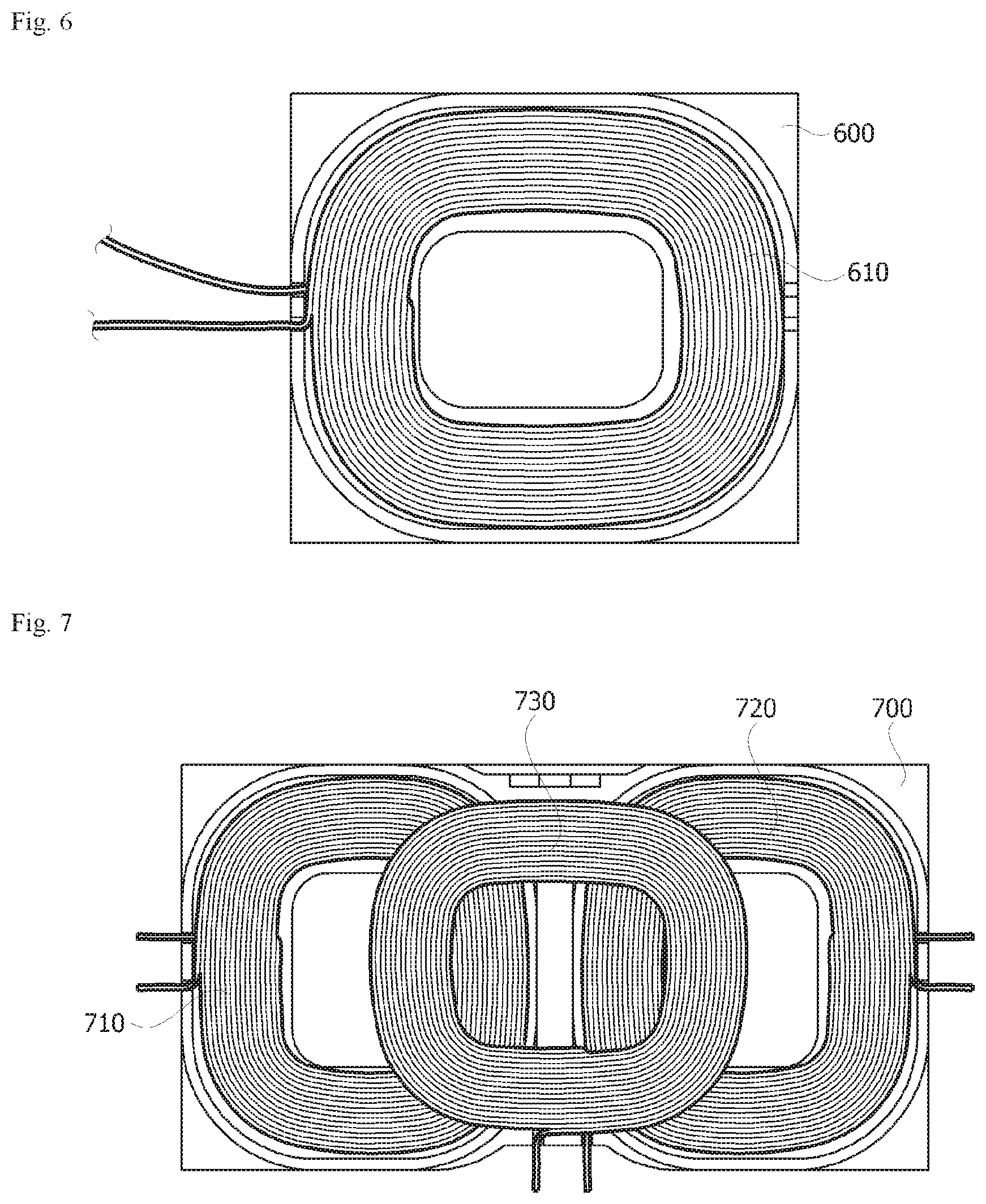
[0065] FIG. 6 is a top view of a soft magnetic layer and a transmitting coil included in a wireless power transmitting apparatus according to an embodiment of the present invention.
[0066] Referring to FIG. 6, a transmitting coil 610 is formed on a soft magnetic layer 600. The transmitting coil 610 may be in a wire wound shape such as a spiral or a helical shape on a plane. Although the transmitting coil 610 may have a round shape, a racetrack shape, a rectangular shape, a triangular shape, or a polygonal shape which has rounded corners, the transmitting coil 610 is not limited to these shapes thereto.
[0067] FIG. 7 is a top view of a soft magnetic layer and a transmitting coil included in a wireless power transmitting apparatus according to another embodiment of the present invention.
[0068] Referring to FIG. 7, transmitting coils 710, 720 and 730 are formed on a soft magnetic layer 700. Each transmitting coil 710, 720 and 730 may be in a wire wound shape such as a spiral or a helical shape on a plane. Although each transmitting coil 710, 720 and 730 may be in a round shape, a racetrack shape, a rectangular shape, a triangular shape or a polygonal shape which has rounded corners, the shapes are not limited thereto. The transmitting coil 710 and the transmitting coil 720 are disposed in parallel, and the transmitting coil 730 may be disposed on the transmitting coil 710 and the transmitting coil 720.
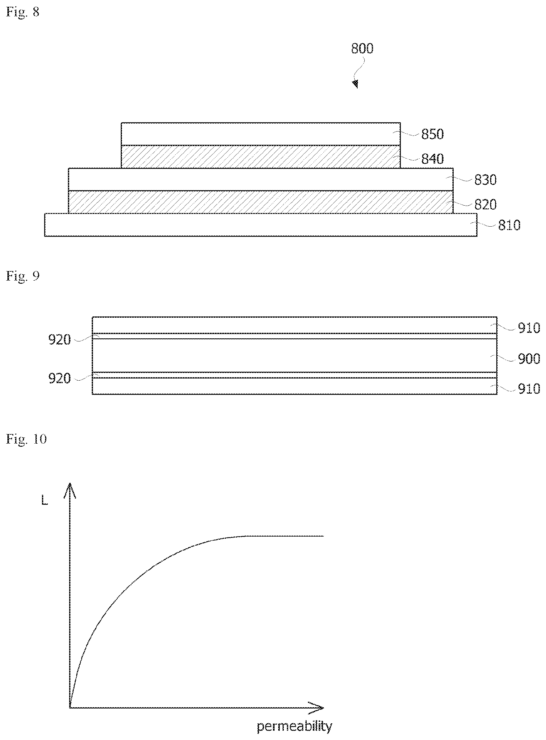
[0069] FIG. 8 is a cross-sectional view of a wireless power transmitting apparatus according to an embodiment of the present invention, and FIG. 9 is a cross-sectional view of a bonding layer included in a wireless power transmitting apparatus according to an embodiment of the present invention.
[0070] Referring to FIG. 8, a wireless power transmitting apparatus 800 includes a substrate 810, a first bonding layer 820 formed on the substrate 810, a soft magnetic layer 830 formed on the first bonding layer 820, a second bonding layer 840 formed on the soft magnetic layer 830 and a transmitting coil 850 formed on the second bonding layer 840.
[0071] The substrate 810 may be a plastic material substrate or a metal material substrate. The substrate 810 may also be a PCB (Printed Circuit Board). The substrate 810 may be a case of the wireless power transmitting apparatus 800. Thus, the substrate 810 may be used with an instrument.
[0072] The soft magnetic layer 830 may be embodied in various forms such as a pellet, a plate, a sheet, a ribbon, a foil, a film, a composite, etc. However, when the wireless power transmitting apparatus 800 is applied to a vehicle, the pellet is difficult to use due to vibration or temperature characteristics of vehicles. Thus, the soft magnetic layer 830 may include a composite comprising a single metal or an alloy powder/flakes and a polymer resin. Here, although the alloy powder/flakes may include at least one of Fe, Co and Ni alloy powder/flakes and Fe, Si and Cr alloy powder/flakes, they are not limited thereto. Further, although the polymer resin may include at least one of a PV (polyvinyl)-based resin, a PE (polyethylene)-based resin and a PP (polypropylene)-based resin, the polymer resin is not limited thereto. In this case, the soft magnetic layer 830 may include 90 wt % or more of an alloy powder/flakes, and 10 wt % or less of a polymer resin.
[0073] The transmitting coil 850 is formed on the soft magnetic layer 830. The coil 850 may be wound in a direction parallel to a plane of the soft magnetic layer 830 on the soft magnetic layer 830. Although it is not shown, a support film may further be formed on the transmitting coil 850. The support film is for supporting the transmitting coil 850, and it may include a PET (polyethylene terephthalate) material.
[0074] Meanwhile, the first bonding layer 820 is formed between the substrate 810 and the soft magnetic layer 830, and bonds the substrate 810 and the soft magnetic layer 830 together. Further, the second bonding layer 840 is formed between the soft magnetic layer 830 and the transmitting coil 850, and bonds the soft magnetic layer 830 and the transmitting coil 850 together. In this case, at least one of the first bonding layer 820 and the second bonding layer 840 includes a magnetic substance. When at least one of the first bonding layer 820 and the second bonding layer 840 includes a magnetic substance, the effective permeability of the wireless power transmitting apparatus 800 may increase, and the inductance may increase.
[0075] Referring to FIG. 9, at least one of the first bonding layer 820 and the second bonding layer 840 includes a magnetic layer 900 and a bonding agent 910 formed on both sides of the magnetic layer.
[0076] The magnetic layer 900 may be a magnetic sheet, a magnetic film, a magnetic foil, etc. that includes a magnetic substance with high permeability. Here, although the magnetic substance with a high permeability may, for example, be a sendust, a permalloy, a MPP (Molybdenum Permalloy Powder), etc., the magnetic substance with high permeability is not limited thereto. The sendust refers to a Fe--Si--Al ternary alloy. The permalloy refers to a Ni--Fe binary alloy. Accordingly, an initial permeability of the magnetic layer 900 may be 500.mu.' or more, and the difference in the initial permeability between the magnetic layer and the soft magnetic layer 830 may be 100.mu.' or more at a range of 100 to 300 kHz. Here, the magnetic layer 900 may replace a dielectric substance film substrate of a general double-sided tape, which bonds the substrate 810 and the soft magnetic layer 830 or the soft magnetic layer 830 and the coil 850. Accordingly, without increasing an overall thickness of the wireless power transmitting apparatus or the wireless power receiving apparatus, it may be possible to increase effective permeability, and to increase inductance.
[0077] In this case, a metal ribbon may further be formed between the magnetic layer 900 and the bonding agent 910. Here, the metal ribbon may refer to a thin film which is made by spreading out a metal very slightly in a single atomic unit. Since the permeability of the metal ribbon is very high, without increasing an overall thickness of the wireless power transmitting apparatus, it may be possible to further increase effective permeability, and to increase inductance.
[0078] Meanwhile, when permeability of the magnetic layer 900 is higher than that of the soft magnetic layer 830, an electromagnetic component may be compensated due to a current conducted between the first bonding layer 820 or the second bonding layer 840 and the soft magnetic layer 830. Accordingly, the bonding agent 910 may include an insulation material. For instance, the bonding agent 910 may include an acrylate-based organic bonding agent, an epoxy-based organic bonding agent, a silicon-based organic bonding agent, etc.
[0079] In other cases, a surface of the first bonding layer 820 or the second bonding layer 840 may be film-forming processed with SiO.sub.2 or the like. Accordingly, the soft magnetic layer 830 may be insulated from the first bonding layer 820 or the second bonding layer 840.
[0080] Hereinafter, a test result related to inductance of a wireless power transmitting apparatus according to an embodiment of the present invention is explained.
[0081] FIG. 10 is a graph, when a bonding layer does not include a magnetic substance, explaining an increasing rate of inductance according to an increase in permeability thereof, and FIG. 11 is a graph, when a bonding layer does not include a magnetic substance, explaining an increasing rate of inductance according to an increase in thickness thereof.
[0082] Referring to FIG. 10 and FIG. 11, the inductance increases up to a certain level as permeability (.mu.') or thickness increases; however, when the inductance arrives at the certain level, it does not increase anymore, but rather is saturated.
[0083] FIG. 12 is a graph, when a bonding layer includes a magnetic substance, explaining an increasing rate of inductance according to an increase in thickness thereof.
[0084] Here, a substrate, a soft magnetic layer and a coil are laminated in a sequence, and a bonding layer is formed between the substrate and the soft magnetic layer and between the soft magnetic layer and the coil. A soft magnetic layer which has permeability (.mu.) of 26 and a thickness of 2.0 mm is used, and a bonding layer between the soft magnetic layer and a coil is fixed at a thickness of 0.1 mm.
[0085] After measuring inductance when a bonding layer does not include a magnetic substance (normal), i.e. when using a general double-sided tape in which a bonding agent is formed on both sides of a substrate made by an dielectric film, the inductance was measured while increasing the thickness of a bonding layer from 0.1 mm to 0.4 mm, wherein the bonding layer included a magnetic substance of which permeability (.mu.) was 500 and a thickness ratio of a magnetic layer and a bonding agent was 7:3.
[0086] As shown in FIG. 12, when the bonding layer includes the magnetic substance (approximately 11.4), it can be found that the inductance is higher than the case that the bonding layer does not include a magnetic substance (approximately 11.2). Further, it can be found that even if a bonding layer including a magnetic substance becomes thicker, the inductance thereof is not saturated, but rather it increases continuously.
[0087] Thus, according to an embodiment of the present invention, a wireless power transmitting apparatus having high inductance may be achieved. Moreover, a desired level of inductance may be achieved by adjusting the thickness of a bonding layer.
[0088] Hereinabove, for the sake of providing a convenient description, although a wireless power transmitting apparatus is described by way of examples, the invention is not limited thereto. Embodiments of the present invention may also be equally applied to a bonding layer which is formed between a substrate, a soft magnetic layer and a coil of a wireless power receiving apparatus. Further, when a wireless power receiving apparatus has a WPC function and NFC function simultaneously, a NFC coil may be further laminated onto a soft magnetic layer. The NFC coil may be configured to surround an outer circumference of a receiving coil.
[0089] Although exemplary embodiments of the present invention have been referenced and described above, it will be understood that it is possible for those of ordinary skill in the art to implement modifications and variations on the present invention without departing from the concept and scope of the present invention listed in the following appended claims.
DESCRIPTION OF REFERENCE NUMERALS
[0090] 10: a wireless charging system [0091] 100: a power source [0092] 200: a wireless power transmitting apparatus [0093] 300: a wireless power receiving apparatus [0094] 810: a substrate [0095] 820 and 840: a bonding layer [0096] 830: a soft magnetic layer [0097] 850: a coil
* * * * *
D00000
D00001
D00002
D00003
D00004
D00005
XML
uspto.report is an independent third-party trademark research tool that is not affiliated, endorsed, or sponsored by the United States Patent and Trademark Office (USPTO) or any other governmental organization. The information provided by uspto.report is based on publicly available data at the time of writing and is intended for informational purposes only.
While we strive to provide accurate and up-to-date information, we do not guarantee the accuracy, completeness, reliability, or suitability of the information displayed on this site. The use of this site is at your own risk. Any reliance you place on such information is therefore strictly at your own risk.
All official trademark data, including owner information, should be verified by visiting the official USPTO website at www.uspto.gov. This site is not intended to replace professional legal advice and should not be used as a substitute for consulting with a legal professional who is knowledgeable about trademark law.