Semiconductor Device With Integrated Shunt Resistor And Method For Producing Same
Sander; Rainald ; et al.
U.S. patent application number 16/399603 was filed with the patent office on 2019-11-14 for semiconductor device with integrated shunt resistor and method for producing same. The applicant listed for this patent is Infineon Technologies AG. Invention is credited to Thomas Bemmerl, Rainald Sander, Steffen Thiele.
| Application Number | 20190348333 16/399603 |
| Document ID | / |
| Family ID | 68336744 |
| Filed Date | 2019-11-14 |


| United States Patent Application | 20190348333 |
| Kind Code | A1 |
| Sander; Rainald ; et al. | November 14, 2019 |
SEMICONDUCTOR DEVICE WITH INTEGRATED SHUNT RESISTOR AND METHOD FOR PRODUCING SAME
Abstract
A semiconductor device comprises a first chip pad, a power semiconductor chip arranged on the first chip pad and comprising at least a first and a second power electrode, and a clip connected to the first power electrode. In this case, an integral part of the clip forms a shunt resistor and a first contact finger of the shunt resistor is embodied integrally with the clip.
| Inventors: | Sander; Rainald; (Oberhaching, DE) ; Bemmerl; Thomas; (Schwandorf, DE) ; Thiele; Steffen; (Munich, DE) | ||||||||||
| Applicant: |
|
||||||||||
|---|---|---|---|---|---|---|---|---|---|---|---|
| Family ID: | 68336744 | ||||||||||
| Appl. No.: | 16/399603 | ||||||||||
| Filed: | April 30, 2019 |
| Current U.S. Class: | 1/1 |
| Current CPC Class: | H01L 21/4825 20130101; H01L 2224/0603 20130101; H01L 23/4952 20130101; H01L 23/49562 20130101; H01L 23/49503 20130101; H01L 2224/40 20130101; H01L 23/49575 20130101; H01L 23/62 20130101; H01L 23/49524 20130101; H01L 22/32 20130101; H01L 22/34 20130101; H01L 2224/48 20130101 |
| International Class: | H01L 21/66 20060101 H01L021/66; H01L 23/495 20060101 H01L023/495; H01L 21/48 20060101 H01L021/48 |
Foreign Application Data
| Date | Code | Application Number |
|---|---|---|
| May 9, 2018 | DE | 102018207308.2 |
Claims
1. A semiconductor device, comprising: a first chip pad; a power semiconductor chip arranged on the first chip pad and comprising at least a first and a second power electrode; and a clip connected to the first power electrode; wherein an integral part of the clip forms a shunt resistor; and wherein a first contact finger of the shunt resistor is embodied integrally with the clip.
2. The semiconductor device according to claim 1, wherein a second contact finger of the shunt resistor is embodied integrally with the clip.
3. The semiconductor device according to claim 1, wherein a distal end of the first contact finger is connected to or forms a first external terminal of the semiconductor device.
4. The semiconductor device according to claim 2, wherein a distal end of the second contact finger is connected to or forms a second external terminal of the semiconductor device.
5. The semiconductor device according to claim 1, wherein a distal end of the first contact finger is connected to a first measurement electrode of a semiconductor voltage measuring unit arranged in the semiconductor device.
6. The semiconductor device according to claim 2, wherein a distal end of the second contact finger is connected to a second measurement electrode of a semiconductor voltage measuring unit arranged in the semiconductor device.
7. The semiconductor device according to claim 5, wherein the semiconductor voltage measuring unit is embodied monolithically with the power semiconductor chip.
8. The semiconductor device according to claim 5, wherein the semiconductor voltage measuring unit comprises a semiconductor chip arranged on a main surface of the power semiconductor chip.
9. The semiconductor device according to claim 5, wherein the semiconductor voltage measuring unit comprises a semiconductor chip arranged laterally next to the power semiconductor chip.
10. The semiconductor device according to claim 1, wherein a distal end of the clip is connected to or forms an external terminal of the semiconductor device.
11. The semiconductor device according to claim 10, wherein the external terminal forms a common power terminal of the power semiconductor chip and measurement terminal for measuring a voltage drop across the shunt resistor.
12. The semiconductor device according to claim 1, further comprising: a second power semiconductor chip arranged on a second chip pad separated from the first chip pad.
13. The semiconductor device according to claim 12, wherein the clip electrically connects the first power electrode of the first power semiconductor chip to the second chip pad.
14. A method for producing a semiconductor device, the method comprising: fitting a power semiconductor chip on a chip pad, wherein the power semiconductor chip comprises at least a first and a second power electrode; and fitting a clip to the first power electrode, wherein an integral part of the clip forms a shunt resistor and wherein a first contact finger of the shunt resistor is embodied integrally with the clip.
15. The method according to claim 14, wherein a second contact finger of the shunt resistor is embodied integrally with the clip.
16. The method according to claim 14, further comprising: providing a semiconductor voltage measuring unit in the semiconductor device; and fitting the first contact finger to a measurement terminal of the semiconductor voltage measuring unit.
17. The method according to claim 15, further comprising: fitting the second contact finger to a further measurement terminal of the semiconductor voltage measuring unit.
18. The method according to claim 14, further comprising: fitting the first contact finger to an external terminal of the semiconductor device.
19. The method according to claim 14, wherein the chip pad is part of a lower leadframe and the clip is part of an upper leadframe.
20. The method according to claim 19, further comprising: fitting a second clip to a control electrode of the power semiconductor chip, wherein the second clip is part of the upper leadframe.
Description
TECHNICAL FIELD
[0001] The present disclosure relates to a semiconductor device with integrated shunt resistor, and to a method for producing a semiconductor device with integrated shunt resistor.
BACKGROUND
[0002] Semiconductor devices can contain power semiconductor chips configured to switch high currents. For numerous applications it may be necessary to determine the intensity of a current flowing through such a power semiconductor chip. Such a determination of the current flow can usually take place externally; by way of example, the semiconductor device can be fitted on a circuit board and be electrically connected to the latter and a measuring device for measuring the current through the power semiconductor chip may be present on the circuit board. For the purpose of an optimized integration density of the semiconductor device, however, it may be advantageous to determine the current internally, i.e. within the semiconductor device itself, e.g. by means of an integrated shunt resistor.
[0003] An object of the invention can therefore be considered that of providing a semiconductor device with an improved integrated shunt resistor. Furthermore, the invention aims to specify a method for producing a semiconductor device with an improved integrated shunt resistor.
[0004] This object is achieved by means of the features of the independent claims. The dependent claims present advantageous configurations of the disclosure.
SUMMARY
[0005] One aspect of the disclosure relates to a semiconductor device, comprising a first chip pad, a power semiconductor chip arranged on the first chip pad and comprising at least a first and a second power electrode, and a clip connected to the first power electrode, wherein an integral part of the clip forms a shunt resistor, and wherein a first contact finger of the shunt resistor is embodied integrally with the clip.
[0006] A further aspect of the disclosure relates to a method for producing a semiconductor device, the method comprising fitting a power semiconductor chip on a chip pad, wherein the power semiconductor chip comprises at least a first and a second power electrode, and fitting a clip to the first power electrode, wherein an integral part of the clip forms a shunt resistor and wherein a first contact finger of the shunt resistor is embodied integrally with the clip.
BRIEF DESCRIPTION OF THE DRAWINGS
[0007] A semiconductor device and a method for producing a semiconductor device in accordance with the disclosure are explained in greater detail below with reference to drawings. The elements shown in the drawings are not necessarily rendered in a manner true to scale relative to one another. Identical reference signs may denote identical components.
[0008] FIG. 1 shows a schematic plan view of a semiconductor device with integrated shunt resistor in accordance with the disclosure.
[0009] FIG. 2 shows a circuit diagram which can be realized e.g. by the semiconductor device from FIG. 1.
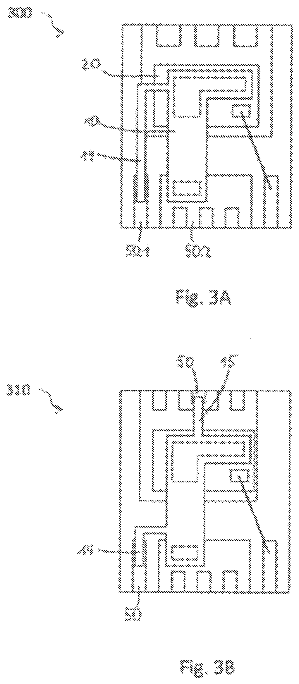
[0010] FIGS. 3A-3C show schematic plan views of further semiconductor devices in accordance with the disclosure, in which one or a plurality of contact fingers of the integrated shunt resistor have different arrangements.
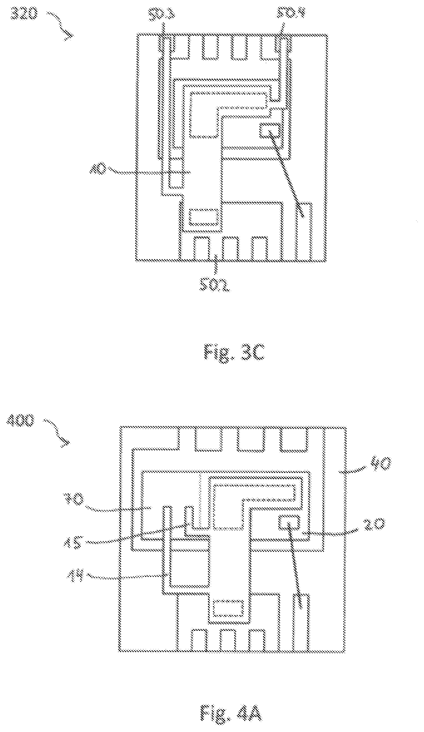
[0011] FIGS. 4A-4C show schematic plan views of further semiconductor devices in accordance with the disclosure, which furthermore comprise an integrated semiconductor voltage measuring unit, which is electrically connected to the contact fingers of the integrated shunt resistor.
[0012] FIG. 5 shows a schematic plan view of a further semiconductor device in accordance with the disclosure, in which the integrated shunt resistor is embodied integrally with external terminals of the semiconductor device.
[0013] FIG. 6 shows a schematic plan view of a further semiconductor device in accordance with the disclosure, in which the clip forming the integrated shunt resistor is used for providing a half-bridge circuit.
[0014] FIG. 7 shows an exemplary flow diagram of a method for producing a semiconductor device with integrated shunt resistor.
DETAILED DESCRIPTION
[0015] In the following detailed description, reference is made to the drawings and the examples shown therein. The terms "fit", "secure" and "connect" together with derivatives thereof may be used. These terms may be used to indicate that two elements cooperate or interact with one another, it being unimportant whether they are in direct physical or electrical contact with one another or are not in direct contact with one another; intermediate elements or layers may be provided between the "fitted", "secured" or "connected" elements or the elements may have direct contact with one another.
[0016] FIG. 1 shows one example of a semiconductor device 100 comprising a clip 10, a power semiconductor chip 20 and a chip pad 30. The power semiconductor chip 20 comprises at least a first and a second power electrode, wherein the clip 10 is electrically connected to the first power electrode. The semiconductor device 100 may furthermore comprise an encapsulation 40 and external terminals 50 exposed at the encapsulation 40. The clip 10 can be completely encapsulated by the encapsulation 40.
[0017] The semiconductor device 100 can be designed for customer-side fitting to a circuit board, e.g. as a surface mounted device or as a through hole device. The semiconductor device 100 can be a semiconductor package. The encapsulation 40 can be an injection-molded body or a laminated body. The external terminals 50 can, as shown in FIGS. 1 and 3A to 6, be embodied such that they do not project beyond an outline contour of the encapsulation (no leads package), or they can project beyond the outline contour (leaded package).
[0018] In accordance with one example, the first power electrode is arranged on an upper main surface of the power semiconductor chip 20 and the second power electrode is arranged on an opposite lower main surface of the power semiconductor chip 20, i.e. the power semiconductor chip 20 is designed for a vertical current flow. The second power electrode can be electrically connected to the chip pad 30. In accordance with one example, the first power electrode can be a source electrode and the second power electrode can be a drain electrode. In accordance with a further example, source and drain electrodes can be interchanged.
[0019] The power semiconductor chip 20 can comprise a control electrode 21, e.g. a gate electrode, which is configured to control a current flow between the power electrodes. The control electrode 21 can be arranged on the upper main surface of the power semiconductor chip 20. The control electrode can be connected to an external terminal 50 of the semiconductor device 100 by an electrical connector 60. The electrical connector 60 can comprise or consist of a bond wire or a clip.
[0020] The clip 10 can be configured to electrically connect the first power electrode of the semiconductor chip 20 to a further element of the semiconductor device 100, e.g. to an external terminal 50 or a further chip pad (not shown in FIG. 1). The clip 10 can comprise or consist of an arbitrary electrically conductive material, e.g. a metal or a metal alloy. The clip 10 can comprise or consist of Al, Cu or Fe, for example. The clip 10 can be embodied in one piece, i.e. from a single continuous piece.
[0021] The clip 10 comprises an integral part 11 forming a shunt resistor or measuring resistor. The shunt resistor is designed to the effect that a current flow through the clip 10 can be measured by way of the voltage drop across the shunt resistor, which is proportional to the current flow.
[0022] The integral part 11 can be arranged between a first contact area 12 and a second contact area 13 of the clip 10, which can be situated at opposite ends of the clip 10. At the first contact area 12, the clip 10 is connected to the first power electrode of the power semiconductor chip 20, e.g. is soldered onto said first power electrode. At the second contact area 13, the clip 10 can be connected to an external terminal 50 or to a further chip pad of the semiconductor device 100. Alternatively, the clip 10 can also itself form an external terminal 50 of the semiconductor device 100; in this case, a second contact area 13 is not present.
[0023] The clip 10 comprises at least a first contact finger 14 of the shunt resistor, wherein the first contact finger 14 is embodied integrally (in one piece) with the clip 10. The first contact finger 14 can project e.g. laterally from the rest of the clip 10. A distal end of the first contact finger 14 can be connected to an external terminal 50 of the semiconductor device 100 or form an external terminal 50.
[0024] In accordance with one example, the clip 10 can furthermore comprise a second contact finger 15 of the shunt resistor, wherein the second contact finger 15 is embodied integrally (in one piece) with the clip 10. A distal end of the second contact finger 15 can be connected to an external terminal 50 of the semiconductor device 100 or form an external terminal 50.
[0025] In accordance with one example, a current flow through the clip 10 can be measured in such a way that the voltage drop across the shunt resistor that is associated with the current flow is tapped off and measured at the contact fingers 14 and 15. In accordance with another example, for instance if the clip comprises only the first contact finger 14 but not the second contact finger 15, the current flow can also be measured in such a way that the voltage drop across the shunt resistor is tapped off and measured at the contact finger 14 and at that external terminal 50 to which the second contact area 13 of the clip 10 is connected.
[0026] The clip 10 can be configured in such a way that the integral part 11 comprises a shunt resistor having a resistor value such that a current flow through the clip 10 can be measured with the application-specifically desired accuracy. For example, the length and/or the thickness and/or the width of the clip 10 can be chosen in such a way that the shunt resistor formed by the integral part 11 has the resistance value required for the desired accuracy. In accordance with one example, a voltage drop across the shunt resistor can be approximately 1 mV.
[0027] FIG. 2 shows an electrical circuit diagram 200 representing one possible electrical circuit of the semiconductor device 100. The circuit diagram 200 comprises a transistor 210 and a shunt resistor 220 connected to a power electrode of the transistor, e.g. a source electrode. The shunt resistor 220 comprises measurement contacts 221, 222 in order to be able to determine a voltage drop across the shunt resistor 220 and thus a current flow through the transistor 210. In the semiconductor device 100, the transistor 210 can be realized by the power semiconductor chip 20, the shunt resistor 220 can be realized by the integral part 11 of the clip 10, and the measurement contacts 221, 222 can be realized by the contact fingers 14, 15. Alternatively, in the case where only the first measurement contact 221 (i.e. the first contact finger 14) is present, but not the second measurement contact 222 (i.e. the second contact finger 15), a power contact 230, e.g. a source contact, of the transistor 210, said power contact corresponding to the external terminal 50, can simultaneously function as a second measurement contact of the shunt resistor 220.
[0028] The subsequent FIGS. 3A to 6 show further examples of semiconductor devices, which can be identical to the semiconductor device 100 apart from the differences shown or described. In particular, what all of the semiconductor devices in accordance with the disclosure have in common is that an integral part of the clip 10 forms a shunt resistor, the shunt resistor comprises at least one contact finger and the at least one contact finger is embodied integrally with the clip 10. Identical reference signs may denote identical components.
[0029] FIGS. 3A to 3C show various possibilities for connecting contact fingers of the shunt resistor to external terminals of the semiconductor device.
[0030] FIG. 3A shows a semiconductor device 300 in which the shunt resistor comprises only a single contact finger 14. A distal end of the contact finger 14 is connected to a first external terminal 50.1 of the semiconductor device 300. A distal end of the clip 10 is connected to a second external terminal 50.2, wherein the second terminal 50.2 forms a common power terminal of the power semiconductor chip 20 and measurement terminal for measuring a voltage drop across the shunt resistor.
[0031] FIG. 3B shows a semiconductor device 310 in which the shunt resistor comprises two contact fingers 14, 15. The contact fingers 14, 15 are connected to external terminals 50 lying on opposite sides of the semiconductor device.
[0032] FIG. 3C likewise shows a semiconductor device 320 in which the shunt resistor comprises two contact fingers 14, 15. One end of the clip 10 is connected to an external terminal 50.2 of the semiconductor device 320. The contact fingers 14, 15 are connected to external terminals 50.3, 50.4 arranged on a side of the semiconductor device 320 that is situated opposite the side having the external terminal 50.2.
[0033] FIGS. 1 and 3A to 3C show semiconductor devices in which the contact finger 14 or respectively the contact fingers 14, 15 is/are connected to external terminals of the semiconductor device. That means that in the exemplary semiconductor devices in FIGS. 1 and 3A to 3C, the voltage drop across the shunt resistor and thus the current flow through the clip 10 is measured externally. In accordance with a further aspect of the disclosure, however, it is also possible for this measurement to take place internally. For this purpose, a semiconductor voltage measuring unit can be arranged in the semiconductor device and the contact fingers 14, 15 can be connected to the semiconductor voltage measuring unit.
[0034] FIGS. 4A to 4C show examples of semiconductor devices comprising an integrated semiconductor voltage measuring snit 70. In accordance with one example, the semiconductor voltage measuring unit 70 can be connected to external terminals of the semiconductor device (not shown in FIG. 4), e.g. in order to communicate the measured voltage drop. The semiconductor voltage measuring unit 70 can be completely encapsulated by the encapsulation 40.
[0035] In accordance with one example, the semiconductor voltage measuring unit 70 can comprise a logic semiconductor component. The semiconductor voltage measuring unit 70 can comprise a bipolar transistor. The semiconductor voltage measuring unit 70 can be realized by CMOS technology.
[0036] FIG. 4A shows a semiconductor device 400 in which the semiconductor voltage measuring unit 70 integrated into the semiconductor device 400 is embodied monolithically with the power semiconductor chip 20 (this is illustrated by the dashed line in FIG. 4A).
[0037] In accordance with one example, the power semiconductor chip 20 can be a p-channel MOSFET. In accordance with another example, the power semiconductor chip 20 can be an n-channel MOSFET.
[0038] FIG. 4B shows a semiconductor device 410 in which the semiconductor voltage measuring unit 70 comprises a dedicated semiconductor chip arranged laterally next to the power semiconductor chip 20 on the chip pad 30. The semiconductor voltage measuring unit 70 can be secured to the chip pad 30 e.g. by means of a solder connection or by means of an adhesive, for instance by means of a non-conductive adhesive.
[0039] FIG. 4C shows a semiconductor device 420 in which the semiconductor voltage measuring unit 70 is arranged on the upper main surface of the power semiconductor chip 20 (chip-on-chip). The semiconductor voltage measuring unit 70 can be secured to the upper main surface of the power semiconductor chip 20 e.g. by means of a solder connection or by means of an adhesive, for instance by means of a non-conductive adhesive.
[0040] FIGS. 1, 3A to 3C and 4A to 4C show semiconductor devices in which the clip 10 and the electrical connector 60 are not embodied integrally with the respective external terminal 50. However, it is also possible for the clip 10, the contact finger 14 or respectively the contact fingers 14, 15 and/or the electrical connector 60 to be embodied integrally with the respective external terminal 50. In other words, the clip 10, the respective contact finger 14 or 14, 15 and/or the electrical connector 60 can itself form the respective external terminal 50.
[0041] FIG. 5 shows a semiconductor device 500 in which the clip 10 and the contact finger 14 are embodied integrally with the respective external terminal 50. Furthermore, the electrical connector 60 is configured as a further clip, which likewise itself forms an external terminal 50.
[0042] In accordance with one example, a method for producing a semiconductor device can comprise applying the clip 10 and/or the electrical connector 60 embodied as a further clip on the power semiconductor chip 20 by means of a pick and place process.
[0043] In accordance with another example, a method for producing a semiconductor device can comprise the chip pad 20 being part or a first (lower) leadframe and the clip 10 and/or the electrical connector 60 embodied as a further clip being part of a second (upper) leadframe. The upper leadframe can be arranged on the upper main surface of the power semiconductor chip 20 and the clip 10 and/or the electrical connector 60 can be singulated from the upper leadframe.
[0044] Such a manner of construction using a first (lower) leadframe and a further upper leadframe (comprising the clip 10 with integral contact finger 14 or respectively integral contact fingers 14, 15 and e.g. the electrical connector 60) can be used in all of the semiconductor devices described here, i.e. in particular also in the semiconductor devices in which the external terminals 50 are realized partly or completely by the lower leadframe (see FIGS. 1 and 3A to 4C).
[0045] In the semiconductor devices in FIGS. 1 and 3A to 5, the clip 10 is configured for electrically connecting the first power electrode of the power semiconductor chip 20 to an external terminal 50. However, it is also possible for the clip 10 to provide an internal electrical connection in the semiconductor device.
[0046] FIG. 6 shows a semiconductor device 600 comprising a first power semiconductor chip 20 and a second power semiconductor chip 610, wherein the first power semiconductor chip 20 is arranged on and electrically connected to a first chip pad 30 and the second power semiconductor chip 610 is arranged on and electrically connected to a second chip pad 620. The clip 10 connects the first power electrode of the first power semiconductor chip 20 (internally) to the second chip pad 620 in a half-bridge circuit.
[0047] In accordance with one example, one of the power semiconductor chips 20, 610 can be an n-channel MOSFET and the other of the power semiconductor chips 20, 610 can be a p-channel MOSFET. The first chip pad 30 and the second chip pad 620 can be referred to as a "lifted" leadframe.
[0048] In accordance with one example, the contact fingers 14, 15 are connected to an internal semiconductor voltage measuring unit (not shown in FIG. 6). In accordance with another example, the contact fingers 14, 15 are connected to external terminals (not shown in FIG. 6) of the semiconductor device 600.
[0049] The semiconductor device 600 can likewise be constructed using a first (lower) leadframe and a further upper leadframe (comprising the clip 10 with integral contact finger 14 or respectively integral contact fingers 14, 15 and e.g. one or a plurality of electrical connectors (not shown in FIG. 6) for contacting the control electrode(s) of the first power semiconductor chip 20 and, if appropriate, of the second power semiconductor chip 610).
[0050] In all of the semiconductor devices, the integral part 11 of the clip 10 forming the shunt resistor can have a particular shaping. By way of example, the integral part 11 can be embodied, in a lateral dimension, as narrower and/or with a smaller thickness than the first and/or second contact area 12, 13 of the clip 10 in order to reduce the cross-sectional area of the clip 10 in the integral part 11 and thereby to increase the voltage drop between the contact fingers 14, 15.
[0051] FIG. 7 shows a method 700 for producing a semiconductor device. The method 700 comprises, in 701, fitting a power semiconductor chip on a chip pad, wherein the power semiconductor chip comprises at least a first and a second power electrode. The method 700 comprises, in 702, fitting a clip to the first power electrode, wherein an integral part of the clip forms a shunt resistor and wherein a first contact finger of the shunt resistor is embodied integrally with the clip.
[0052] In accordance with one example, the chip pad can be part of a lower leadframe and the clip can be part of an upper leadframe. Furthermore, the method 700 can comprise fitting a second clip to a control electrode of the power semiconductor chip, wherein the second clip is part of the upper leadframe.
EXAMPLES
[0053] The semiconductor device and the method for producing a semiconductor device are explained in greater detail below on the basis of examples.
[0054] Example 1 is a semiconductor device, comprising a first chip pad, a power semiconductor chip arranged on the first chip pad and comprising at least a first and a second power electrode, and a clip connected to the first power electrode, wherein an integral part of the clip forms a shunt resistor, and wherein a first contact finger of the shunt resistor is embodied integrally with the clip.
[0055] Example 2 is a semiconductor device according to Example 1, wherein a second contact finger of the shunt resistor is embodied integrally with the clip.
[0056] Example 3 a semiconductor device according to Example 1 or 2, wherein a distal end of the first contact finger is connected to or forms a first external terminal of the semiconductor device.
[0057] Example a semiconductor device according to Example 2, wherein a distal end of the second contact finger is connected to or forms a second external terminal of the semiconductor device.
[0058] Example 5 is a semiconductor device according to Example 1, wherein a distal end of the first contact finger is connected to a first measurement electrode of a semiconductor voltage measuring unit arranged in the semiconductor device.
[0059] Example 6 is a semiconductor device according to Example 2, wherein a distal end of the second contact finger is connected to a second measurement electrode of a semiconductor voltage measuring unit arranged in the semiconductor device.
[0060] Example 7 is a semiconductor device according to Example 5 or 6, wherein the semiconductor voltage measuring unit is embodied monolithically with the power semiconductor chip.
[0061] Example 8 is a semiconductor device according to Example 5 or 6, wherein the semiconductor voltage measuring unit comprises a semiconductor chip arranged on a main surface of the power semiconductor chip.
[0062] Example 9 is a semiconductor device according to Example 5 or 6, wherein the semiconductor voltage measuring unit comprises a semiconductor chip arranged laterally next to the power semiconductor chip.
[0063] Example 10 is a semiconductor device according to Example 1, wherein a distal end of the clime is connected to or forms an external terminal of the semiconductor device.
[0064] Example 11 is a semiconductor device according to Example 10, wherein the external terminal forms a common power terminal of the power semiconductor chip and measurement terminal for measuring a voltage drop across the shunt resistor.
[0065] Example 12 is a semiconductor device according to Example 1, furthermore comprising a second power semiconductor chip arranged on a second chip pad separated from the first chip pad.
[0066] Example 13 is a semiconductor device according, to Example 12, wherein the clip electrically connects the first power electrode of the first power semiconductor chip to the second chip pad.
[0067] Example 14 is a method for producing a semiconductor device, the method comprising fitting a power semiconductor chip on a chip pad, wherein the power semiconductor chip comprises at least a first and a second power electrode, and fitting a clip to the first power electrode, wherein an integral part of the clip forms a shunt resistor and wherein a first contact finger of the shunt resistor is embodied integrally with the clip.
[0068] Example 15 is a method according to Example 14, wherein a second contact finger of the shunt resistor is embodied integrally with the clip.
[0069] Example 16 is a method according to Example 14 or 15, furthermore comprising providing a semiconductor voltage measuring unit in the semiconductor device, and fitting the first contact finger to a measurement terminal of the semiconductor voltage measuring unit.
[0070] Example 17 is a method according to Examples 15 and 16, furthermore comprising fitting the second contact finger to a further measurement terminal of the semiconductor voltage measuring unit.
[0071] Example 18 is a method according to Example 14 or 15, furthermore comprising fitting the first contact finger to an external terminal of the semiconductor device.
[0072] Example 19 is a method according to any of Examples 14 to 18, wherein the chip pad is part of a lower leadframe and the clip is part of an upper leadframe.
[0073] Example 20 is a method according to Example 19, furthermore comprising fitting a second clip to a control electrode of the power semiconductor chip, wherein the second clip is part of the upper leadframe.
LIST OF REFERENCE SIGNS
[0074] 10 clip [0075] 11 integral part of the clip [0076] 12 first contact area [0077] 13 second contact area [0078] 14 first contact finger [0079] 15 second contact finger [0080] 20 power semiconductor chip [0081] 21 control electrode [0082] 30 chip pad [0083] 40 encapsulation [0084] 50 external terminals [0085] 50.1 external terminal [0086] 50.2 external terminal [0087] 50.3 external terminal [0088] 50.4 external terminal [0089] 60 electrical connector [0090] 70 semiconductor voltage measuring unit [0091] 100 semiconductor device [0092] 200 circuit diagram [0093] 210 transistor [0094] 220 shunt resistor [0095] 221 measurement contact [0096] 222 measurement contact [0097] 230 power contact [0098] 300 semiconductor device [0099] 310 semiconductor device [0100] 320 semiconductor device [0101] 400 semiconductor device [0102] 410 semiconductor device [0103] 420 semiconductor device [0104] 500 semiconductor device [0105] 600 semiconductor device [0106] 610 second power semiconductor chip [0107] 620 second chip pad [0108] 700 method for producing a semiconductor device [0109] 701 fitting a power semiconductor chip [0110] 702 fitting a clip
* * * * *
D00000
D00001
D00002
D00003
D00004
D00005
D00006
XML
uspto.report is an independent third-party trademark research tool that is not affiliated, endorsed, or sponsored by the United States Patent and Trademark Office (USPTO) or any other governmental organization. The information provided by uspto.report is based on publicly available data at the time of writing and is intended for informational purposes only.
While we strive to provide accurate and up-to-date information, we do not guarantee the accuracy, completeness, reliability, or suitability of the information displayed on this site. The use of this site is at your own risk. Any reliance you place on such information is therefore strictly at your own risk.
All official trademark data, including owner information, should be verified by visiting the official USPTO website at www.uspto.gov. This site is not intended to replace professional legal advice and should not be used as a substitute for consulting with a legal professional who is knowledgeable about trademark law.