Capacitor Discharge Circuit
Snyder; Benjamin J. ; et al.
U.S. patent application number 15/965070 was filed with the patent office on 2019-10-31 for capacitor discharge circuit. This patent application is currently assigned to Raytheon Company. The applicant listed for this patent is Raytheon Company. Invention is credited to Aline Elad, Erin K. Nolan, Benjamin J. Snyder, John D. Walker.
| Application Number | 20190334363 15/965070 |
| Document ID | / |
| Family ID | 66102770 |
| Filed Date | 2019-10-31 |


| United States Patent Application | 20190334363 |
| Kind Code | A1 |
| Snyder; Benjamin J. ; et al. | October 31, 2019 |
CAPACITOR DISCHARGE CIRCUIT
Abstract
A capacitor discharge circuit for discharging a capacitor to a discharge load. The discharge circuity includes current level sensing circuitry for producing a control signal circuity response to current passing to the discharge load. The discharge circuity modulates a level of current passing from the capacitor to the discharge load over time between predetermined ranges of current levels in response to the control signal.
| Inventors: | Snyder; Benjamin J.; (Boxborough, MA) ; Nolan; Erin K.; (Bolton, MA) ; Elad; Aline; (Ayer, MA) ; Walker; John D.; (Bolton, MA) | ||||||||||
| Applicant: |
|
||||||||||
|---|---|---|---|---|---|---|---|---|---|---|---|
| Assignee: | Raytheon Company Waltham MA |
||||||||||
| Family ID: | 66102770 | ||||||||||
| Appl. No.: | 15/965070 | ||||||||||
| Filed: | April 27, 2018 |
| Current U.S. Class: | 1/1 |
| Current CPC Class: | H02M 1/32 20130101; H02J 7/345 20130101; H02J 7/0063 20130101; H02J 2007/0067 20130101; H02M 3/156 20130101 |
| International Class: | H02J 7/00 20060101 H02J007/00 |
Claims
1. A capacitor discharge circuit, comprising: a capacitor; a discharge load; a controller, responsive to a control signal, for coupling the discharge load to the capacitor in response to a discharge command signal; discharge circuity, comprising current level sensing circuitry for producing a control signal circuity in response to current passing to the discharge load, for modulating a level of current passing from the capacitor to the discharge load over time between predetermined ranges of current levels in response to the control signal.
2. A capacitor discharge circuit, comprising: a capacitor; a discharge load; discharge circuity, comprising current level sensing circuitry for producing a control signal circuity response to current passing to the discharge load, the discharge circuity, for discharging the capacitor to the discharge load over a plurality of discharge cycles, with current from the capacitor passing through the discharge load with increasing level over time during one portion of each one of the discharge cycles and with current passing through the discharge load decreasing in level over time during a different portion of each one of the discharge cycles in response to the control signal.
3. The capacitor discharge circuit recited in claim 2 wherein the discharge circuitry includes an inductor in series with both the capacitor and discharge load, wherein: during said one portion of each one of the discharge cycles, the inductor stores a portion of energy discharged from the capacitor while a different portion of the energy discharged is dissipated in the discharge load; and during said different portion of each one of the discharge cycles the portion of the energy stored in the inductor is dissipated in the discharge load.
4. The capacitor discharge circuit recited in claim 3 wherein the discharge circuity comprising: current level sensing circuitry for sensing the level of the current passing to the discharge load during said one portion of each one of the discharge cycles; and a controller for initiating switching from said one portion of each one of the discharge cycles to said different one of the discharge cycles when the level of the sensed current passing through a predetermined current level.
5. The capacitor discharge circuit recited in claim 4 wherein the discharge circuity includes timing circuity for switching from said one portion of each one of the discharge cycles to said different one of each one of the discharge cycles a predetermined period of time after the initiating switching from said one portion of each one of the discharge cycles to said different one of the discharge cycles.
6. The capacitor discharge circuit recited in claim 5 wherein the current level sensing circuitry produces a voltage level varying in accordance with the level of current passing through the discharge load during said one portion of each one of the discharge cycles and wherein the discharge circuity comprises a voltage sampler, responsive to current level sensing circuitry, for storing a sample of the level of the produced voltage level when such produced voltage level reaches a predetermined voltage level; a resistor-capacitor network fed by the sampler, the capacitor of the resistor-capacitor network storing the sample of the produced voltage level and then discharging the stored voltage through the resistor of such resistor-capacitor network; and circuitry for initiating said different portion of each one of the discharge cycles when the voltage discharges to a second predetermined voltage level;
7. A capacitor discharge circuit, comprising: a capacitor connected having a first plate and a second plate for storing an electric charge; discharge circuitry connected between the first plate and the second plate, comprising: a discharge section having one terminal connected to the first plate, the discharge section comprising: discharge load; an inductor serially connected to the discharge load; a diode connected in parallel with the serially connected discharge load and the inductor; a switch; and current level sensing circuitry; wherein the discharge section, switch, and current level sensing circuitry are serially connected the first plate and the second plate; and a controller, responsive to a control signal, for enabling the electric charge to become discharged from such capacitor and dissipated in the discharge load; and wherein, in response to the control signal, a first one of a plurality of discharge cycles is initiated and wherein: during a first phase of the plurality of discharge cycles: the switch is closed electrically coupling the discharge section to the second plate with current passing from the first plate through discharge load, through the inductor, through the closed switch and through the current level sensing circuitry with such current producing a voltage to reverse bias the diode, a portion of energy in such current being dissipated in the discharge load and another portion of such energy such current being stored in a magnetic field of the inductor until the current reaches a predetermined level sensed by the current level sensing circuitry to initiate a second phase of the plurality of discharge cycles; and during a second phase of the plurality of discharge cycle: the switch is open electrically interrupting current from passing from the first plate through the inductor with such interrupted current resulting in the inductor producing a voltage to forward bias the diode and enable the energy stored in the magnetic field of the inductor to pass to the discharge load and dissipate in the discharge load and, subsequent to such discharge, initiate a subsequent one of the plurality of discharge cycles.
Description
TECHNICAL FIELD
[0001] This disclosure relates generally to capacitor discharge circuits and more particularly, to capacitor discharge circuits for dissipating a constant amount of energy stored in the capacitor during the discharge of the capacitor.
BACKGROUND
[0002] As is known in the art, many applications require the discharge of capacitors storing relatively high voltages, for example greater than thirty volts, and as high as 90 volts or more in less than a few seconds. One techniques used to discharge capacitors is to couple the capacitor to a high energy rated resistor that is switched across the capacitor in response to a control signal applied when the discharge is required. However, such an arrangement results in a very large instantaneous peak power dissipation that rolls off as the voltage reduces as a function of the RC time constant requiring the resistor to operate continuously with high power and limit restart cycles in order to provide sufficient cooling time for the resistor. More particularly, the resistors thin the stored energy into heat causing the surrounding temperature to rise. Power cannot be reapplied until the resistors and surrounding circuitry has sufficiently cooled. The discharge resistors are also subject to overheating and destruction if main power is still applied while the discharge circuit is active. Lastly, the power dissipated by the resistor is non-linear, that is as the voltage across the energy storage elements decays, the power dissipated rolls off as a function of the decreasing voltage squared, which causes the resistor to be sized much larger than it would otherwise be if the power were linearly dissipated over the discharge time.
[0003] Other capacitor discharge circuits are suggested in Chinese Patents CN 102593812A and CN202495761U, such circuits being constant power discharge circuits using pulse width modulation to create a constant voltage across a discharge resistor.
SUMMARY
[0004] In accordance with the disclosure, a capacitor discharge circuit is provided having: a capacitor; a discharge load; a controller, responsive to a control signal, for coupling the discharge load to the capacitor in response to a discharge command signal; and discharge circuity, comprising current level sensing circuitry for producing a control signal in response to current passing to the discharge load, the discharge circuity modulating a level of current passing from the capacitor to the discharge load over time between predetermined ranges of current levels in response to the control signal.
[0005] In one embodiment the discharge circuity comprises current level sensing circuitry for producing a control signal circuity in response to current passing to the discharge load, the discharge circuity discharging the capacitor to the discharge load over a plurality of discharge cycles with current from the capacitor passing through the discharge load with increasing in level over time during one portion of each one of the discharge cycles and with current passing through the discharge load decreasing in level over time during a different portion of each one of the discharge cycles in response to the control signal.
[0006] In one embodiment, the discharge circuitry includes an inductor in series with both the capacitor and discharge load, wherein: during said one portion of each one of the discharge cycles, the inductor stores a portion of energy discharged from the capacitor while a different portion of the energy discharged is dissipated in the discharge load; and during said different portion of each one of the discharge cycles the portion of the energy discharged stored in the inductor is dissipated in the discharge load.
[0007] In one embodiment, the discharge circuity comprises: current level sensing circuitry for sensing the level of the current passing to the discharge load during said one portion of each one of the discharge cycles; and a controller for initiating switching from said one portion of each one of the discharge cycles to said different one of the discharge cycles when the level of the sensed current passing through a predetermined current level.
[0008] In one embodiment, the discharge circuity includes timing circuity for switching from said one portion of each one of the discharge cycles to said different one of each one of the discharge cycles a predetermined period of time after the initiating switching from said one portion of each one of the discharge cycles to said different one of the discharge cycles.
[0009] In one embodiment, the current level sensing circuitry produces a voltage level varying in accordance with the level of current passing through the discharge load during said one portion of each one of the discharge cycles and wherein the discharge circuity comprises: a voltage sampler, responsive to current level sensing circuitry, for storing a sample of the level of the produced voltage level when such produced voltage level reaches a predetermined voltage level; a resistor-capacitor network fed by the sampler, the capacitor of the resistor-capacitor network storing the sample of the produced voltage level and then discharging the stored voltage through the resistor of such resistor-capacitor network; and circuitry for initiating said different portion of each one of the discharge cycles when the voltage discharges to a second predetermined voltage level;
[0010] In one embodiment, a capacitor discharge circuit is provided, comprising: a capacitor connected having a first plate and a second plate for storing an electric charge; and discharge circuitry connected between the first plate and the second plate. The discharge circuitry, comprising: a discharge section having one terminal connected to the first plate. The discharge section comprising: discharge load; an inductor serially connected to the discharge load; a diode connected in parallel with the serially connected discharge load and the inductor; a switch; and current level sensing circuitry. The discharge section, switch, and current level sensing circuitry are serially connected the first plate and the second plate. A controller, responsive to a control signal, enables the electric charge to become discharged from such capacitor and dissipated in the discharge load. In response to the control signal, a first one of a plurality of discharge cycles is initiated. During a first phase of the plurality of discharge cycles: the switch is closed electrically coupling the discharge section to the second plate with current passing from the first plate through discharge load, through the inductor, through the closed switch and through the current level sensing circuitry with such current producing a voltage to reverse bias the diode, a portion of energy in such current being dissipated in the discharge load and another portion of such energy such current being stored in a magnetic field of the inductor until the current reaches a predetermined level sensed by the current level sensing circuitry to initiate a second phase of the plurality of discharge cycles; and during a second phase of the plurality of discharge cycle: the switch is open electrically interrupting current from passing from the first plate through the inductor with such interrupted current resulting in the inductor producing a voltage to forward bias the diode and enable the energy stored in the magnetic field of the inductor to pass to the discharge load and dissipate in the discharge load and, subsequent to such discharge, initiate a subsequent one of the plurality of discharge cycles.
[0011] With such an arrangement, a capacitor discharge circuit is provided which enables constant dissipation of the energy stored in a capacitor bank and thereby allows for the use of smaller dissipation resistors, reapplication of main input power at any time after discharge; and can be operated indefinitely if a failure of the discharge circuit or power system occurs that causes the discharge circuit to be active while main system power is still applied to the capacitor bank. The constant power discharge is achieved by the creation of an average current through the discharge resistors by use of an inductor and freewheeling flyback diode. Control of the discharge circuit current can be achieved by a plurality of methods such as matching the RC time constant of a comparator monitoring circuit to the L/R time constant of the discharge circuit, and turning a FET switch on and off at the appropriate time. The circuit is self-powered from the voltage of the capacitor bank that is being discharged so external power is not required for operation.
[0012] The constant discharge is achieved by turning the FET switch "on" when the current through the inductor reaches the lower peak, and turning the FET "off" when the current reaches the high peak. That switching of the FET "on" and "off" creates a triangular waveform of current through the inductor and discharge resistor, which results in a constant (average) power dissipation in the resistors.
[0013] Thus, the disclosure provides for the constant dissipation of the energy stored in a capacitor, which allows for the use of smaller dissipation resistors, reapplication of main input power at any time after discharge; and, can be operated indefinitely if a failure of the discharge circuit or power system occurs that causes the discharge circuit to be active while main system power is still applied to the capacitor bank. The constant power discharge is achieved by the creation of an average current through the discharge resistors by use of an inductor and freewheeling flyback diode. The circuit is self-powered from the voltage of the capacitor bank that is being discharged so external power is not required for operation. The circuit greatly reduces the physical size and energy rating of the energy dissipating elements (resistors), provides a failsafe control in the event an active discharge command while the power was applied, is more reliable, and is scalable to large system level designs.
[0014] The details of one or more embodiments of the disclosure are set forth in the accompanying drawings and the description below. Other features, objects, and advantages of the disclosure will be apparent from the description and drawings, and from the claims.
BRIEF DESCRIPTION OF DRAWINGS
[0015] FIG. 1 is a block diagram of a system having a capacitor discharge circuit used to discharge a voltage on a capacitor bank of such system according to the disclosure;
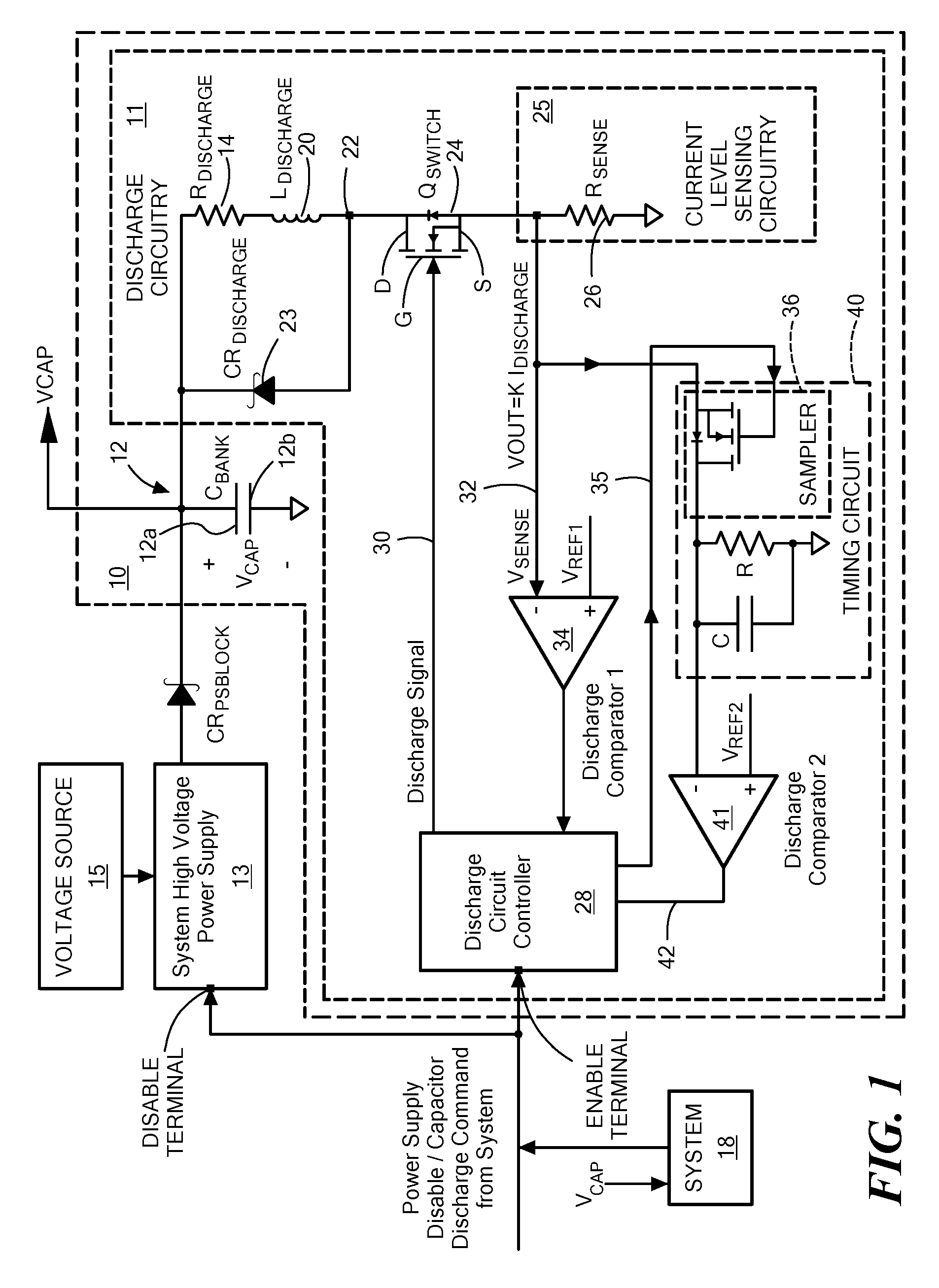
[0016] FIG. 1A is a block diagram of the system of FIG. 1 showing a path for discharge current during a first cycle of one of a plurality of two-phase successive two-phase discharge cycles performed by such capacitor discharge circuit of FIG. 1 according to the disclosure;
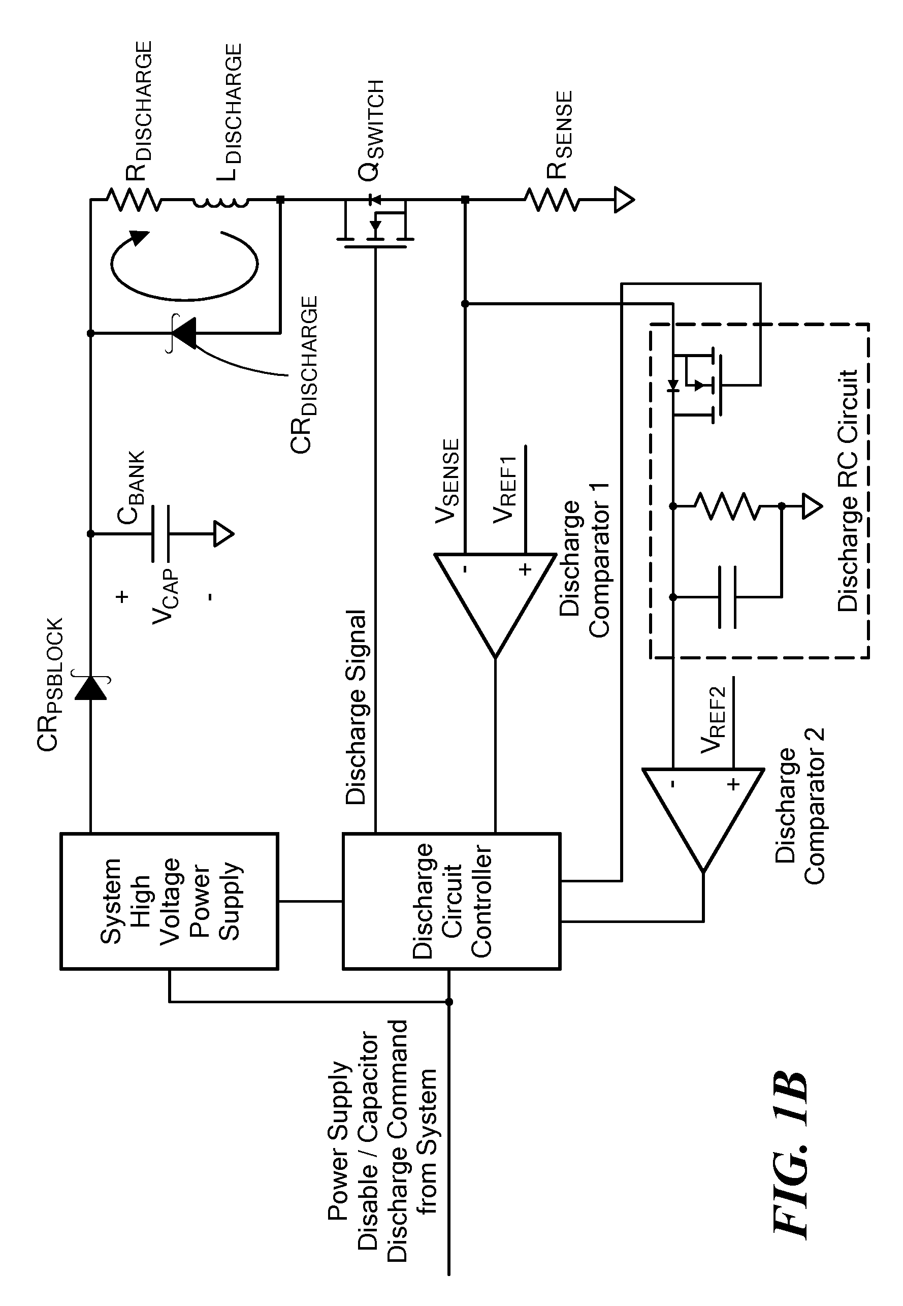
[0017] FIG. 1B is a block diagram of the system of FIG. 1 showing a path for discharge current during a second, subsequent cycle of the one of a plurality of two-phase successive two-phase discharge cycles performed by such capacitor discharge circuit of FIG. 1 according to the disclosure;
[0018] FIG. 2 is a flowchart of the operation of the capacitor discharge circuit of FIG. 1 according to the disclosure
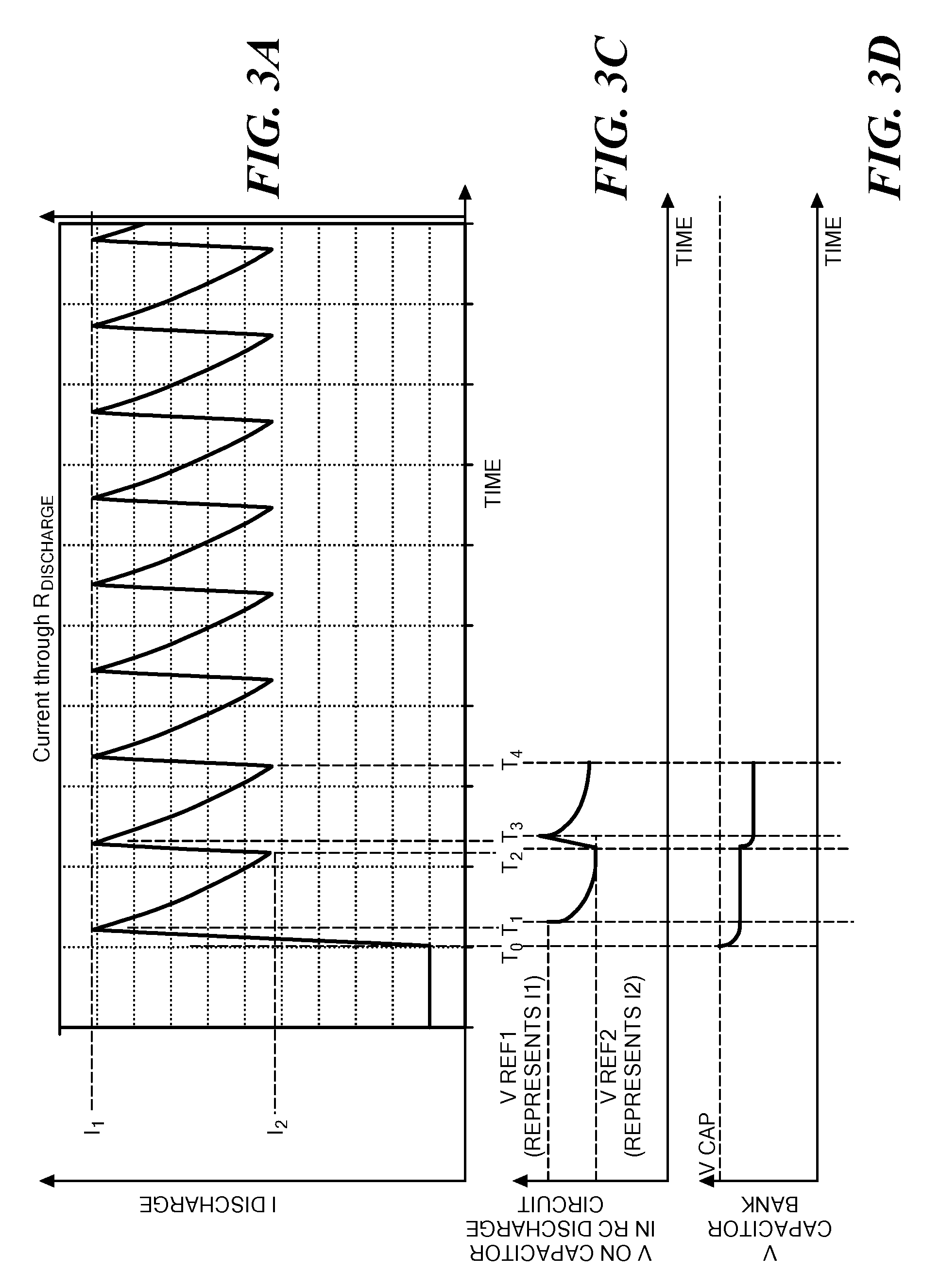
[0019] FIG. 3A is a timing diagram of discharge current through a discharge resistor R.sub.DISCHARGE used in the system of FIG. 1 during a portion of the operation of the capacitor discharge circuit of FIG. 1;
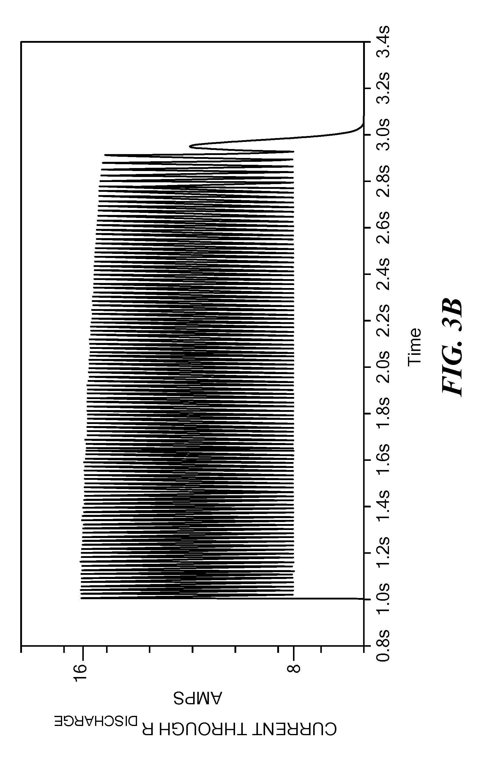
[0020] FIG. 3B is a timing diagram of discharge current through a discharge resistor R.sub.DISCHARGE used in the system of FIG. 1 during the entire operation of the capacitor discharge circuit of FIG. 1;
[0021] FIG. 3C is a timing diagram of a voltage on a capacitor used in an RC circuit used in the system of FIG. 1 during a portion of the operation of the capacitor discharge circuit of FIG. 1;
[0022] FIG. 3D is a timing diagram of a voltage on the capacitor bank being discharged in the system of FIG. 1 during a portion of the operation of the capacitor discharge circuit of FIG. 1; and
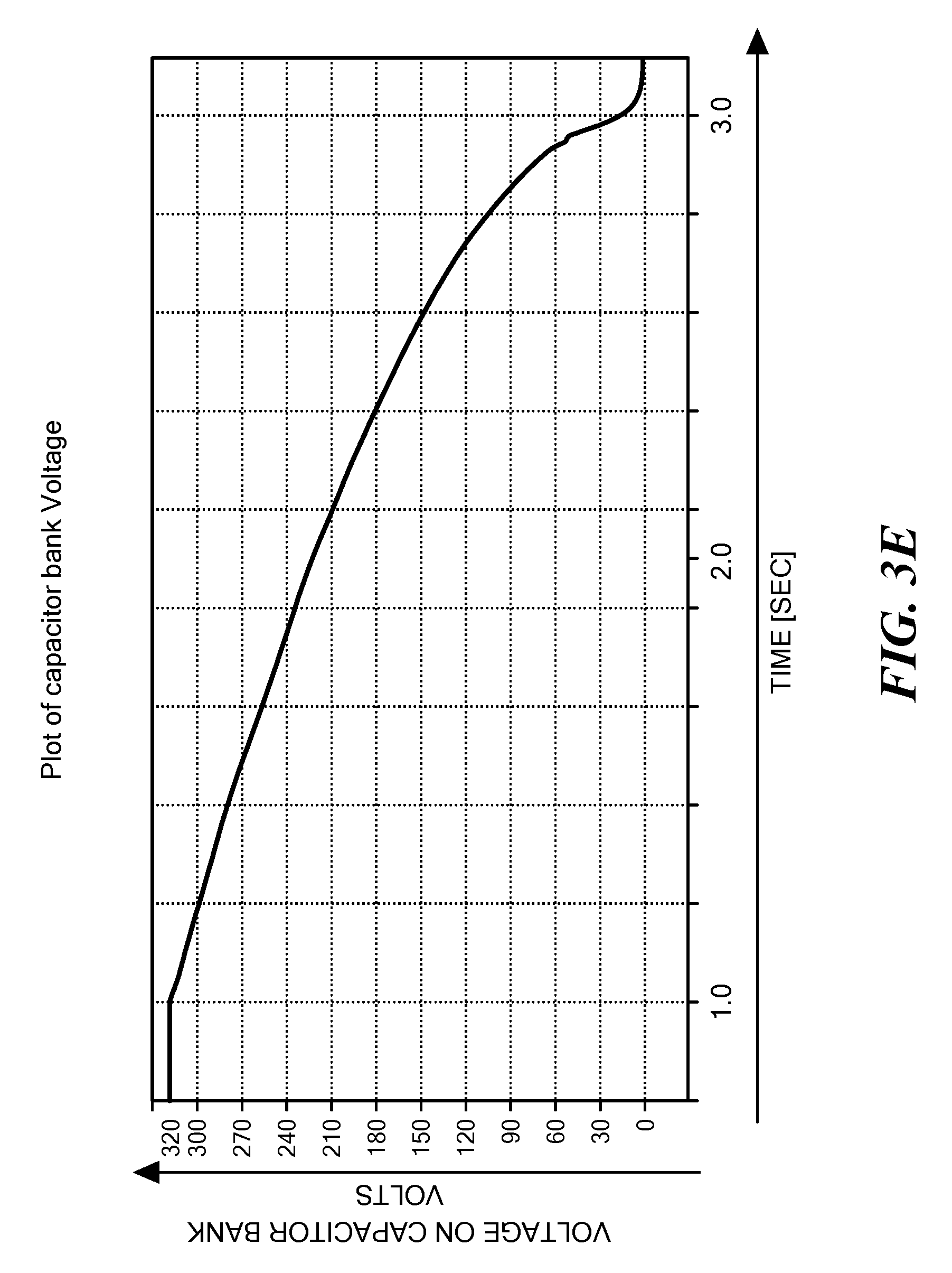
[0023] FIG. 3E is a timing diagram of a voltage on the capacitor bank being discharged in the system of FIG. 1 during the entire operation of the capacitor discharge circuit of FIG. 1,
[0024] Like reference symbols in the various drawings indicate like elements.
DETAILED DESCRIPTION
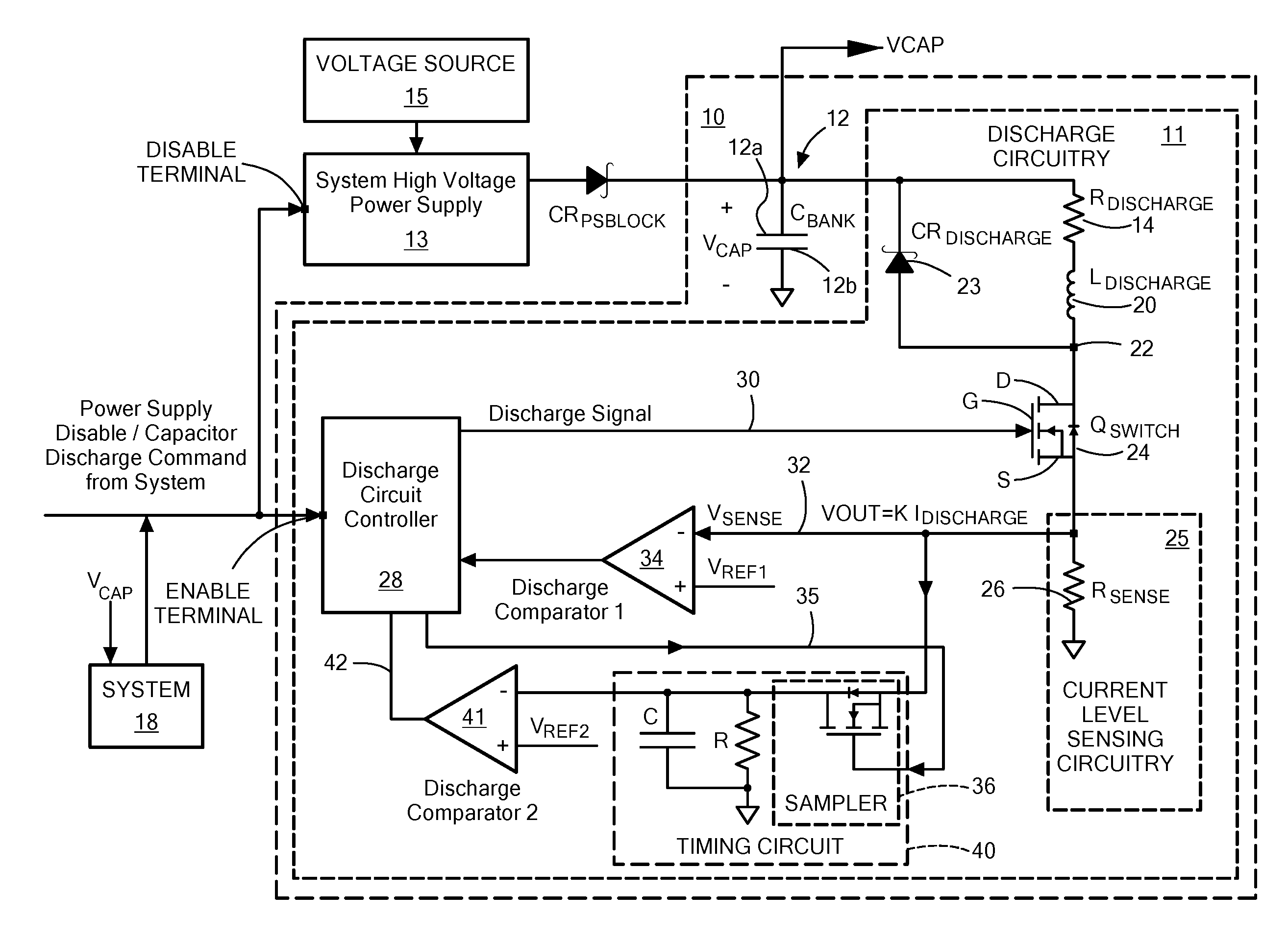
[0025] Referring now to FIG. 1, a circuit 10 is shown having discharge circuitry 11 for discharging a capacitor bank 12, coupled to an output of a High Voltage Power Supply 13, to a discharge load 14, here a resistor R.sub.DISCHARGE, here, for example, 2.5 ohms. The capacitor bank 12 provides a voltage, VCAP, for a system 18. The High VOLTAGE POWER Supply 13 is coupled to a voltage source 15. The voltage source 15 may be: an ac voltage source, in which case the High Voltage Power Supply 13 would, when enabled, produce a DC Voltage at output 17; or, a DC voltage, in which case the High Voltage Power Supply 13 would be a DC-DC converter to increase the DC voltage to a higher DC voltage at output 17. In either case, the DC voltage at output 17 is fed to the Capacitor bank 12 through a diode CR.sub.PSBLOCK, as shown.
[0026] As will be described in more detail below, subsequent to High Voltage Power Supply being enabled and charge being stored on the capacitor bank 12, the discharge circuity 11 discharges such stored change during a plurality of two-phase discharge cycles. More particularly, the discharge circuity 11 is enabled and the charge built up on the capacitor 12 is discharged and thereby dissipated in the discharge load 14 over the plurality of the two-phase discharge cycles, with current from the capacitor bank 12 passing through the discharge load 14 with increasing level over time during one portion, or phase, of each one of the two-phase discharge cycles and with current passing through the discharge load 14 decreasing in level over time during a subsequent, different portion, or phase of each one of the two-phase discharge cycles. In this way, the energy (charge) stored on the capacitor bank 12 is discharged in small packets distributed over a long period of time.
[0027] More particularly, the capacitor bank 12 has one plate or electrode 12b connected to a reference potential, here ground, and the other plate, or electrode, 12a connected to one end of the discharge load 14, as shown. The other end of the discharge load 14 is connected to one end of an inductor L.sub.DISCHARGE 20, here, for example, 60 micro-henries, as shown; the other end of the inductor 20 being connected to a terminal 22, as shown. The terminal 22 is connected to: plate 12a of the capacitor bank 12 through a freewheeling, fly-back diode 23, as shown; and to the drain D of a Field Effect Transistor (FET) Q.sub.SWITCH 24, as shown. The source S of the FET 24 is coupled to ground through a current level sensing resistor R.sub.SENSE 26, as shown.
[0028] The Discharge circuitry 11 includes a discharge controller 28, as shown. In response to a power supply disable/capacitor bank discharge signal from system 18, to the disable terminal of power supply 13 and the enable terminals of controller 28, the voltage produced by the power supply 13 when previously enabled, is decoupled from output terminal 17 and the controller 28 changes a previous state of a signal on line 30 to the gate G of FET 24 from a signal that placed the FET 24 in a non-conducting condition when the power supply 13 was enabled to a state that places FET 24 in a conducting condition and thereby commences the first phase of the two-stage discharge cycle. When PET 24 conducts, charge on plate 12a of capacitor bank 12 passes as discharge current through discharge load 14, inductor 20, FET 24, current level sensing resistor 26 to ground, as shown in FIG. 1A, thereby initiating the first portion or phase of one of a plurality of two-phase discharge cycles. During this portion or phase of the cycle, the discharge current from the capacitor bank 12 passes through the discharge load 14, inductor 20 and sensing resistor 26 increase in level over time. The level of the discharge current from the capacitor bank 12 is sensed by current level sensing circuitry 25, here a sensing resistor 26 which produces a voltage (V.sub.SENSE) on line 32 proportional to such sensed current level. When the voltage V.sub.SENSE reaches a predetermined voltage V.sub.REF1 (such voltage V.sub.REF1 being the voltage level when V.sub.SENSE corresponds to a current level I1 passing thorough R resistor 26 (which is the same current level passing through R.sub.DISCHARGE 14), here, for example, V.sub.REF1 is 1.24 volts), the controller 28 produces the discharge signal on line 30 to place FET 24 in a non-conducting condition. It is noted that during this first portion or first phase of the discharge cycle: (1) While a portion of the energy produced from the discharge current passing from the from the capacitor bank 12 through the discharge load 14 was dissipated in the discharge load 14 another portion of the energy produced from the discharge current passing from the capacitor bank 12 through the discharge load 14 was stored in the magnetic field of inductor 20; (2) the voltage on the capacitor bank 12 was reduced; and (3), the controller 28 sends a sampling pulse on line 35 to sampler 36 of a timing circuit 40 and a capacitor C of the timing circuit 40 stores the sampled voltage V.sub.SENSE.
[0029] When the FET 24 is placed in the non-conducting state, the second portion or phase of the two-phase discharge cycle commences. Three things should be noted during this second portion or phase of the two-stage discharge cycle: (1) energy stored in the inductor 20 during the first portion or cycle of the two-phase discharge cycle, produced from the discharge current passing from the capacitor bank 12 through the discharge load 14, now produces a very high positive induced voltage, sometimes referred to as an inductive kick as a result of rapidly producing at open circuit when the FET 24 is placed in the non-conducting state. This very high positive induced voltage forward biases the diode 23 and the energy stored in the inductor 20 from the discharge current passing from the capacitor bank 12 now passes as current through diode 23 to the discharge load 14, as shown in FIG. 1B, for dissipation in such discharge load 14; and (2) the level of the current through the discharge load 14 decreases over time unlike the increasing level of current passing through the discharge load 14 during the first portion or phase of the two-phase discharge cycle; and (3) the timing circuit 40 sets the time duration of the second portion or phase of the two-phase discharge cycle since the voltage V.sub.REF1 stored on capacitor C, here for example, 0.012 pico-farards, discharges through a resistor R, here for example, 2 KOhms, of the timing circuit 40 and when such voltage on the capacitor C decreases to a predetermined level V.sub.REF2, comparator 41 (the voltage V.sub.REF2 being selected to corresponding to a time determined a priori to be when the level of the current passing though the discharge load 14 reaches a current level 12, here for example, V.sub.REF2 is 0.62 volts) produces a voltage on line 42 to terminate the second portion or phase of the two-phase discharge cycle. More particularly, the controller 28 switches the state of the discharge signal on line 30 to again place the FET 24 in a conducting condition to commence the first portion or phase of the next two phase discharge cycle.
[0030] The operation is summarized in the flowchart of FIG. 2. As noted above, the voltage on the capacitor bank 12 (FIG. 1) decreases in level after each one of the two-phase discharge cycles and when the level of the voltage on the capacitor bank 12 ceases to be at a level sufficient to produce a current having a level I1, the FET 24 remains in the conducting condition and the capacitor bank 12 continues to discharge through the discharge load 14 until all charge is removed from the capacitor bank 12, as shown by the timing diagrams in FIGS. 3 and 4.
[0031] Thus, it is noted that a constant discharge is achieved by turning the FET 24 "on" (in a conducting condition) when the current through the inductor 14 reaches the lower peak and turning the FET 24 "off" (in a non-conducting condition) when the current reaches the high peak. That switching of the FET 24 "on" and "off" creates a triangular waveform of current through the inductor and discharge resistor (FIGS. 3A-3E), which results in a constant (average) power dissipation in the discharge load 14.
[0032] Thus, referring again to FIGS. 3A-3E, to begin the high voltage capacitor discharge at time T.sub.0, a discharge command is applied from the system 18 to the Discharge Circuit Controller 28. The discharge command signal is the inverse of the system power supply 13 enable signal, so that the System High Voltage Power Supply 13 is disabled at the same time that the discharge circuit 11 is enabled. This prevents an active discharge while the System High Voltage Power Supply 13 is still operating. The Discharge Circuit Controller 28 turns on the discharge FET 24, Q.sub.SWITCH, by applying a voltage to the gate G. The voltage on the high voltage capacitor bank 12 C.sub.BANK, causes a current through the discharge load 14 R.sub.DISCHARGE, the discharge inductor L.sub.DISCHARGE, the discharge FET 24 Q.sub.SWITCH, and current sense resistor R.sub.SENSE to begin to increase as it passes to the ground of the circuit. When the current sense voltage V.sub.SENSE created by the discharge current I.sub.DISCHARGE times R.sub.SENSE reaches a reference voltage V.sub.REF1, then the comparator circuit 34 is tripped and FET 24 Q.sub.SWITCH is turned off by the Discharge Circuit Controller 28 at time T.sub.1. Here, for example R.sub.SENSE is 0.08 Ohms. This occurs when the discharge current I.sub.DISCHARGE reaches I.sub.1. The current I.sub.DISCHARGE through R.sub.DISCHARGE and L.sub.DISCHARGE then begins to conduct through the freewheeling, fly-back diode 23 CR.sub.DISCHARGE. The current I.sub.DISCHARGE decays at a rate proportional to the time constant L.sub.DISCHARGE/R.sub.DISCHARGE. The timing circuit 40, here an R-C circuit with a time constant that matches the L.sub.DISCHARGE/R.sub.DISCHARGE time constant samples the voltage V.sub.SENSE at time T.sub.1. Here, V.sub.SENSE changes based on the current through R.sub.SENSE and here V.sub.SENSE peaks at, in this example, 1.4 Volts. When the voltage of the RC circuit timing circuit 40 decays to the trip threshold V.sub.REF2, FET 24 Q.sub.SWITCH is turned on (time T.sub.2 with I.sub.DISCHARGE at I.sub.2), and the cycle repeats with the current I.sub.DISCHARGE once again passing through Q.sub.SWITCH and R.sub.SENSE, and increasing until it reaches the current level I.sub.1 again. Note that the voltage V.sub.CAP on the capacitor bank C.sub.BANK decreases each cycle during the time that FET Q.sub.SWITCH is turned on (e.g. time periods T.sub.0 to T.sub.1 and T.sub.2 to T.sub.3). Because of this, the time it takes for the current I.sub.DISCHARGE to ramp up to the Q.sub.SWITCH turn off threshold I.sub.1 each cycle is slightly longer than the previous cycle by the relationship I.sub.DISCHARGE=(V.sub.CAP/R.sub.DISCHARGE)* (1-exp(-R.sub.DISCHARGE*t/L.sub.DISCHARGE)), where t is time. This means that the frequency of operation of the circuit decreases slightly as the voltage V.sub.CAP decays.
[0033] In the fashion described above an average current is created through resistor R.sub.DISCHARGE and inductor L.sub.DISCHARGE, and thereby an average power is dissipated in discharge load 14 R.sub.DISCHARGE by the square of I.sub.DISCHARGE times R.sub.DISCHARGE. It is also noted that the high current level (I.sub.1) decreases slightly each switching cycle because the voltage on the capacitor bank 12 has decreased slightly from the cycle before. This means that the current increases at a slightly lower rate than the previous cycle. There is a little bit of overshoot on the current each time because current is still flowing through the FET 24 switch as it is being turned "off". The higher voltage on the capacitor bank 12 at the beginning of the discharge makes the current overshoot a little bit more than at the end of the discharge, when the voltage on the capacitor bank 12 is lower. The low switching current (I.sub.2) changes a little bit on the bottom side. However, since a lower peak current was reached, the decay in absolute terms of amps is slightly slower at the end of the discharge than at the beginning, so the change in the lower current level (I.sub.2) is less pronounced that the higher current level (I1). As noted above, the discharge cycles continue until the voltage on C.sub.BANK 12 is insufficient to cause the current through R.sub.SENSE to reach the level of I.sub.1. This means that the FET Q.sub.SWITCH remains turned "on", and the current I.sub.DISCHARGE decays to zero at which time the voltage on capacitor C.sub.BANK also reaches zero. This completes the discharge of the high voltage capacitor C.sub.BANK.
[0034] A number of embodiments of the disclosure have been described. Nevertheless, it will be understood that various modifications may be made without departing from the spirit and scope of the disclosure. Accordingly, other embodiments are within the scope of the following claims.
* * * * *
D00000
D00001
D00002
D00003
D00004
D00005
D00006
D00007
XML
uspto.report is an independent third-party trademark research tool that is not affiliated, endorsed, or sponsored by the United States Patent and Trademark Office (USPTO) or any other governmental organization. The information provided by uspto.report is based on publicly available data at the time of writing and is intended for informational purposes only.
While we strive to provide accurate and up-to-date information, we do not guarantee the accuracy, completeness, reliability, or suitability of the information displayed on this site. The use of this site is at your own risk. Any reliance you place on such information is therefore strictly at your own risk.
All official trademark data, including owner information, should be verified by visiting the official USPTO website at www.uspto.gov. This site is not intended to replace professional legal advice and should not be used as a substitute for consulting with a legal professional who is knowledgeable about trademark law.