Display Device And Method Of Manufacturing The Same
SONG; Yanqin ; et al.
U.S. patent application number 16/313619 was filed with the patent office on 2019-10-24 for display device and method of manufacturing the same. The applicant listed for this patent is KUNSHAN GO-VISIONOX OPTO-ELECTRONICS CO., LTD., KUNSHAN NEW FLAT PANEL DISPLAY TECHNOLOGY CENTER CO., LTD.. Invention is credited to Siming HU, Yanqin SONG, Nan YANG, Jiuzhan ZHANG.
| Application Number | 20190326334 16/313619 |
| Document ID | / |
| Family ID | 62557951 |
| Filed Date | 2019-10-24 |

| United States Patent Application | 20190326334 |
| Kind Code | A1 |
| SONG; Yanqin ; et al. | October 24, 2019 |
DISPLAY DEVICE AND METHOD OF MANUFACTURING THE SAME
Abstract
A display device and a method of manufacturing the same are disclosed. The display device includes a substrate (100), and a patterned polysilicon layer, a patterned gate insulating layer and a patterned first conductive layer stacked on the substrate in sequence. The patterned polysilicon layer includes a number of polysilicon blocks (110) doped with impurities. The patterned first conductive layer includes a number of data lines (120) each partially overlapping a corresponding polysilicon block to form a compensating capacitor.
| Inventors: | SONG; Yanqin; (Jiangsu, CN) ; HU; Siming; (Jiangsu, CN) ; YANG; Nan; (Jiangsu, CN) ; ZHANG; Jiuzhan; (Jiangsu, CN) | ||||||||||
| Applicant: |
|
||||||||||
|---|---|---|---|---|---|---|---|---|---|---|---|
| Family ID: | 62557951 | ||||||||||
| Appl. No.: | 16/313619 | ||||||||||
| Filed: | December 12, 2017 | ||||||||||
| PCT Filed: | December 12, 2017 | ||||||||||
| PCT NO: | PCT/CN2017/115604 | ||||||||||
| 371 Date: | December 27, 2018 |
| Current U.S. Class: | 1/1 |
| Current CPC Class: | G09G 2300/08 20130101; G09G 2300/0426 20130101; G09G 3/20 20130101; H01L 27/1255 20130101; G09G 3/3685 20130101; G09G 2310/0267 20130101; H01L 27/124 20130101; G09G 2300/0408 20130101; H01L 27/127 20130101 |
| International Class: | H01L 27/12 20060101 H01L027/12 |
Foreign Application Data
| Date | Code | Application Number |
|---|---|---|
| Dec 13, 2016 | CN | 201611147363.3 |
Claims
1. A display device, comprising: a substrate; and a patterned polysilicon layer, a patterned gate insulating layer and a patterned first conductive layer, stacked on the substrate in sequence, the patterned polysilicon layer comprising a plurality of polysilicon blocks doped with impurities, the patterned first conductive layer comprising a plurality of data lines, each of the plurality of data lines partially overlapping a corresponding polysilicon block of the plurality of polysilicon blocks to form a compensating capacitor.
2. The display device of claim 1, further comprising a plurality of pixel cells each comprising a thin film transistor and a pixel capacitor, the patterned polysilicon layer further comprises a plurality of sources and drains of the thin film transistors of the plurality of pixel cells and a plurality of first plates of the pixel capacitors of the plurality of pixel cells, and the patterned first conductive layer further comprises a plurality of gates of the thin film transistors of the plurality of pixel cells and a plurality of second plates of the pixel capacitors of the plurality of pixel cells.
3. The display device of claim 2, further comprising a plurality of test circuits, wherein each of the data lines has a first end connected to a corresponding pixel cell of the plurality of pixel cells and a second end connected to a corresponding test circuit of the plurality of test circuits.
4. The display device of claim 2, further comprising a plurality of gate-in-panel circuits, a plurality of pixel connection lines and a plurality of power lines, the plurality of pixel connection lines and power lines being situated in a same layer and made of a same material, the plurality of power lines being connected to the plurality of pixel cells to provide the plurality of pixel cells with a power supply signal, the plurality of pixel connection lines connecting the plurality of pixel cells to the plurality of gate-in-panel circuits.
5. The display device of claim 3, wherein the compensating capacitor is provided to compensate for a parasitic capacitance of the data line, and a compensating capacitance of the compensating capacitor is proportional to an overlapped area of the data line and the polysilicon block.
6. The display device of claim 5, wherein the overlapped area of the data line and the polysilicon block is related to a number of the pixel cells connected to the data line.
7. A method for manufacturing a display device, comprising: providing a substrate; forming a polysilicon layer on the substrate; patterning the polysilicon layer to form a plurality of polysilicon blocks; implanting ions into the plurality of polysilicon blocks; forming a gate insulating layer over the plurality of polysilicon blocks; forming a first conductive layer on the gate insulating layer; and patterning the first conductive layer to form a plurality of data lines, each of plurality of data lines partially overlapping a corresponding polysilicon block of the polysilicon blocks to form a compensating capacitor.
8. The method for manufacturing a display device of claim 7, further comprising, during the patterning the polysilicon layer to form a plurality of polysilicon blocks, patterning the polysilicon layer to form a plurality of first plates of a plurality of pixel capacitors and a plurality of sources and drains of a plurality of thin film transistors.
9. The method for manufacturing a display device of claim 8, further comprising, during the implanting ions into the plurality of polysilicon blocks, implanting ions into the first plates of the plurality of pixel capacitors.
10. The method for manufacturing a display device of claim 8, further comprising, during patterning the first conductive layer to form a plurality of data lines, patterning the first conductive layer to form a plurality of second plates of the plurality of pixel capacitors and a plurality of gates of the plurality of thin film transistors.
11. The method for manufacturing a display device of claim 7, further comprising, subsequent to the patterning the first conductive layer to form a plurality of data lines, forming a second conductive layer over the patterned first conductive layer and patterning the second conductive layer to form a plurality of pixel connection lines and a plurality of power lines.
12. The method for manufacturing a display device of claim 11, further comprising, prior to the forming a second conductive layer over the patterned first conductive layer and subsequent to the patterning the first conductive layer to form the plurality of data lines, forming a plurality of contact holes in the polysilicon blocks for connecting the power lines to the polysilicon blocks.
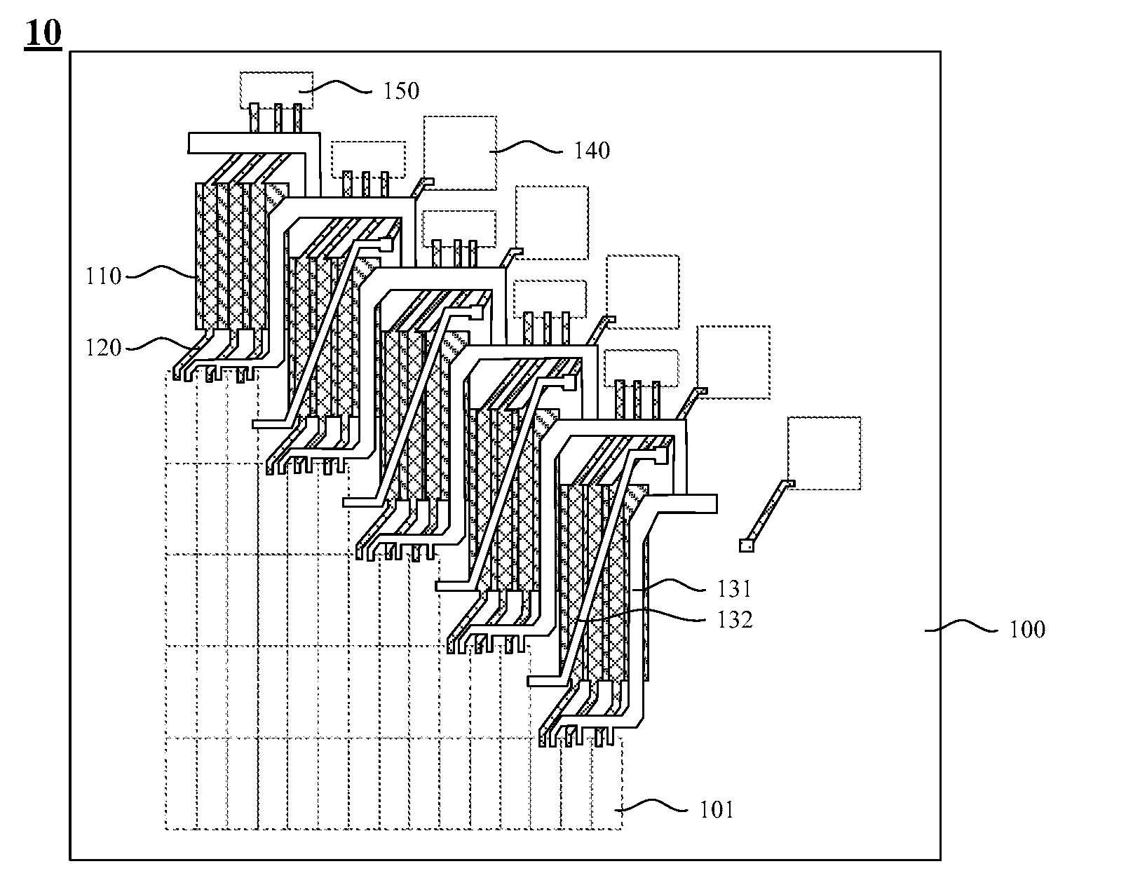
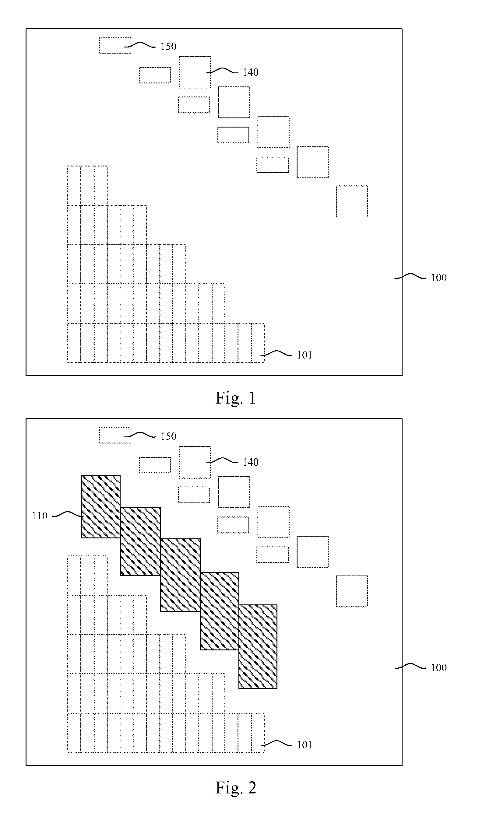
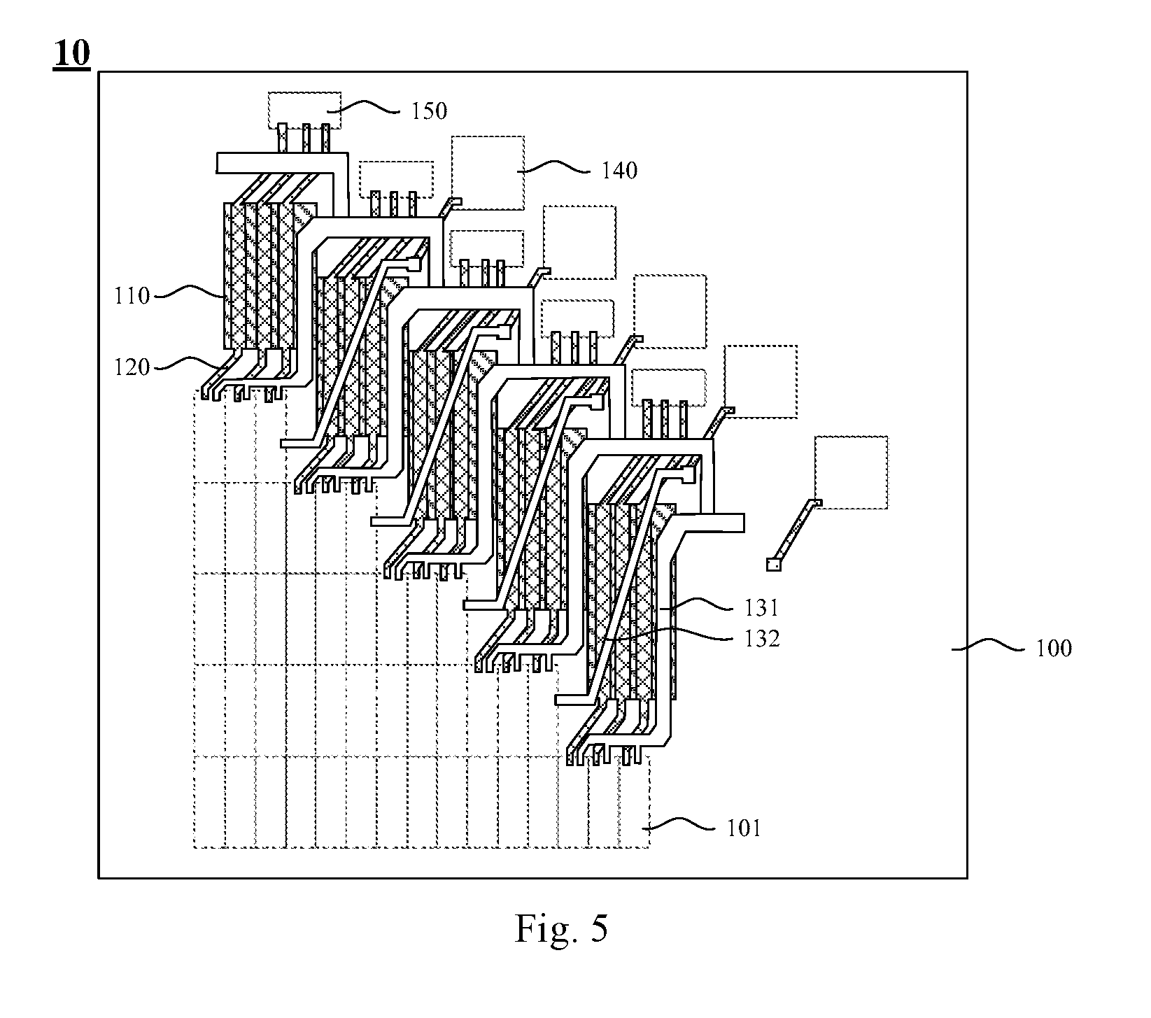
13. The method for manufacturing a display device of claim 7, wherein an overlapped area of the data line and the polysilicon block is determined by a number of pixel cells connected to the data line.
14. The method for manufacturing a display device of claim 13, wherein the overlapped area of the data line and the polysilicon block is inversely related to the number of pixel cells connected to the data line.
Description
TECHNICAL FIELD
[0001] The present invention relates to the field of display technology and, in particular, to a display device and a method for fabricating the display device.
BACKGROUND
[0002] In recent years, the rapid development and increasingly broad application of information technology, wireless mobile communications and information appliances are increasing our dependence on electronic products and have brought about the development of various display technologies and a boom in the field of display devices. Due to the advantages of completely flat, lightweight, slim and power-efficient, the display devices are being widely used.
[0003] In the manufacturing of a lower-cost narrow-bezel display device, the gate-in-panel (GIP) technology is often adopted to directly integrate gate drive circuits (i.e., GIP circuits) in a display panel consisting typically of a display area for displaying images and a non-display area surrounding the display area. In the display area, a plurality of scan lines and a plurality of data lines crossing the scan lines are arranged, thus defining an array of pixel cells. The GIP circuits are provided in the non-display area and are connected to the pixel cells via the scan lines.
[0004] With the development of display technology, display panels are increasingly diversified in terms of shape. As a result, in addition to the traditional rectangular ones, there are also display panels having different shapes such as polygonal and circular. For example, watches typically use circular display panels. In a rectangular display panel, the number of pixels in each column and in each row is the same. However, it is impossible for a polygonal or circular display panel, as the number of pixels may vary across different columns or rows in such display panels.
[0005] Data lines associated with pixel columns containing different numbers of pixels will be inconsistent with one another in terms of parasitic capacitance, which may lead to display unevenness of the display device and necessitates the use of compensating capacitors for parasitic capacitance compensation so as to improve display evenness. However, compensating capacitors employed in conventional display devices have bulky footprints, which hinder the connection between scan lines and GIP circuits and are unfavorable for a narrow bezel.
[0006] Therefore, there is an urgent need in the art for a solution to hindered connection between scan lines and GIP circuits in conventional display devices due to excessively large footprints of compensating capacitors used therein.
SUMMARY OF THE INVENTION
[0007] It is an object of the present invention to provide a display device and a method for fabricating it, which entail a solution to hindered connection between scan lines and GIP circuits in conventional display devices due to excessively large footprints of compensating capacitors used therein.
[0008] To this end, the present invention provides a method for manufacturing a display device, comprising:
[0009] providing a substrate;
[0010] forming a polysilicon layer on the substrate;
[0011] patterning the polysilicon layer to form a plurality of polysilicon blocks;
[0012] implanting ions into the plurality of polysilicon blocks;
[0013] forming a gate insulating layer over the plurality of polysilicon blocks;
[0014] forming a first conductive layer on the gate insulating layer; and
[0015] patterning the first conductive layer to form a plurality of data lines each of plurality of data lines partially overlapping a corresponding polysilicon block of the polysilicon blocks so as to form the plurality of compensating capacitors.
[0016] Optionally, the method may further comprise, during the patterning the polysilicon layer to form a plurality of polysilicon blocks, patterning the polysilicon layer to form a plurality of first plates of a plurality of pixel capacitors and a plurality of sources and drains of a plurality of thin film transistors.
[0017] Optionally, the method may further comprise, during the implanting ions into the plurality of polysilicon blocks, implanting ions into the first plates of the plurality of pixel capacitors.
[0018] Optionally, the method may further comprise, during patterning the first conductive layer to form a plurality of data lines, patterning the first conductive layer to form a plurality of second plates of the plurality of pixel capacitors and a plurality of gates of the plurality of thin film transistors.
[0019] Optionally, the method may further comprise, subsequent to the patterning the first conductive layer to form a plurality of data lines, forming a second conductive layer over the patterned first conductive layer and patterning the second conductive layer to form a plurality of pixel connection lines and a plurality of power lines.
[0020] Optionally, the method may further comprise, prior to the forming a second conductive layer over the patterned first conductive layer and subsequent to the patterning the first conductive layer to form a plurality of data lines, forming a plurality of contact holes in the polysilicon blocks for connecting of the power lines to the polysilicon blocks.
[0021] Optionally, in the method, for each of the data lines, an overlapped area of the data line and the polysilicon block may be adjusted based on a number of pixel cells connected to the data line.
[0022] Optionally, in the method, the smaller the number of pixel cells connected to the data line is, the greater the overlapped area of the data line and the corresponding polysilicon block may be. Additionally, the greater the number of pixel cells connected to the data line is, the smaller the overlapped area between the data line and the corresponding polysilicon block may be.
[0023] In the present invention, there is also provided a corresponding display device, comprising a substrate; and a patterned polysilicon layer, a patterned gate insulating layer and a patterned first conductive layer, stacked on the substrate in sequence, wherein the patterned polysilicon layer comprises a plurality of polysilicon blocks doped with impurities, the patterned first conductive layer comprising a plurality of data lines, each of the plurality of data lines partially overlapping a corresponding polysilicon block of the plurality of polysilicon blocks to form a compensating capacitor.
[0024] Optionally, the display device may further comprise a plurality of pixel cells each comprising a thin film transistor and a pixel capacitor, wherein sources and drains of the thin film transistors and first plates of the plurality of pixel capacitors are fabricated in the same process as the polysilicon blocks, and wherein gates of the thin film transistors and second plates of the pixel capacitors are fabricated in the same process as the data lines.
[0025] Optionally, the display device may further comprise a plurality of test circuits, wherein each of the data lines has a first end connected to a corresponding pixel cell of the plurality of pixel cells and a second end connected to a corresponding test circuit of the test circuits.
[0026] Optionally, the display device may further comprise a plurality of GIP circuits, a plurality of pixel connection lines and a plurality of power lines, the pixel connection lines and the power lines being situated in the same layer and made of the same material, the power lines being connected to the pixel cells and configured to provide pixel cells with a power supply signal, the pixel connection lines being configured to connect the pixel cells to the GIP circuits.
[0027] Optionally, in the display device, the compensating capacitor may be provided to compensate for a parasitic capacitance of the data line, and wherein a compensating capacitance of the compensating capacitor is proportional to an overlapped area of the data line and the polysilicon block.
[0028] Optionally, in the display device, the overlapped area of the data line and the polysilicon block may be related to a number of the pixel cells connected to the data line.
[0029] In summary, in the display device and the method of the present invention, the overlapped area between the doped polysilicon layer and the first conductive layer provides a compensating capacitor for the data line, so that a footprint of the compensating capacitor is reduced and hence the connection between the scan line and GIP circuit is facilitated.
BRIEF DESCRIPTION OF THE DRAWINGS
[0030] FIG. 1 schematically illustrates a structure resulting from a first step in a method for manufacturing a display device according to an embodiment of the present invention.
[0031] FIG. 2 schematically illustrates a structure resulting from a third step in a method for manufacturing a display device according to an embodiment of the present invention.
[0032] FIG. 3 schematically illustrates a structure resulting from a sixth step in a method for manufacturing a display device according to an embodiment of the present invention.
[0033] FIG. 4 schematically illustrates a structure resulting from a contact hole fabrication process in a method for manufacturing a display device according to an embodiment of the present invention.
[0034] FIG. 5 schematically illustrates a structure resulting from the patterning of a second conductive layer in a method for manufacturing a display device according to an embodiment of the present invention.
DETAILED DESCRIPTION
[0035] The present invention will be described in greater detail below with reference to specific embodiments which are to be read in conjunction with the accompanying drawings. Features and advantages of the invention will be more readily apparent from the following detailed description and from the drawings which are presented in a very simplified form not necessarily presented to scale, with the only intention to facilitate convenience and clarity in explaining the embodiments.
[0036] With combined reference to FIGS. 1 to 5, a method for manufacturing a display device according to the present invention includes the steps of:
[0037] 1) providing a substrate 100;
[0038] 2) forming a polysilicon layer on the substrate 100;
[0039] 3) patterning the polysilicon layer to form a plurality of polysilicon blocks 110;
[0040] 4) implanting ions into the polysilicon blocks 110;
[0041] 5) forming a gate insulating layer (not shown) over the plurality of polysilicon blocks 110;
[0042] 6) forming a first conductive layer on the gate insulating layer; and
[0043] 7) patterning the first conductive layer to form a plurality of data lines 120, the plurality of data lines 120 partially overlapping the polysilicon blocks 110 to provide compensating capacitors.
[0044] Specifically, first of all, as shown in FIG. 1, a substrate 100 is provided. The substrate 100 includes a display area and a non-display area surrounding the display area. The display area is formed with a pixel array including a plurality of pixel cells 101 arranged in a pattern of array. Each pixel cell 101 has a pixel capacitor and a thin film transistor (not shown). The non-display area is formed with a plurality of GIP circuits 140 and test circuits 150.
[0045] Subsequently, as shown in FIG. 2, a polysilicon layer is formed on the substrate 100 and patterned by an etching process to form a plurality of first plates (not shown) of the pixel capacitors in the pixel cells 101, sources and drains (not shown) of the thin film transistors in the pixel cells 101, and a plurality of polysilicon blocks 110 outside the pixel cells 101. In the embodiment illustrated in FIG. 2, the polysilicon blocks 110 are formed between the pixel cells 101 and the test circuits 150. Preferably, the polysilicon blocks 110 are all formed in the non-display area.
[0046] Next, boron or phosphorus ions are implanted into the first plates of the pixel capacitors and into the polysilicon blocks 110. The first plate and the polysilicon block 110 are doped by ion implantation, the conductivity of the first plates and polysilicon blocks 110 are improved.
[0047] After that, a gate insulating layer is formed over the patterned polysilicon layer and is then patterned.
[0048] Thereafter, as shown in FIG. 3, a first conductive layer is formed over the patterned gate insulating layer and is then patterned by an etching process to form second plates (not shown) of the pixel capacitors, gates (not shown) of the thin film transistors and a plurality of data lines 120. Each of the data lines 120 is connected to a corresponding one of the pixel cells 101 at one end and to a corresponding one of the test circuits 150 at the other end. The data lines 120 partially overlap a corresponding one of the polysilicon blocks 110 to provide a compensating capacitor.
[0049] The compensating capacitor has a capacitance proportional to an overlapped area of the data line 120 and the polysilicon block 110.
[0050] In this embodiment, the overlapped area of the data line 120 and the polysilicon block 110 could be adjusted according to the number of pixel cells 101 in connection with the corresponding data line 120. The fewer pixel cells 101 connected to the data line 120 are, the smaller parasitic capacitance the data line 120 will have, and hence the greater compensating capacitance will be required to be provided by the compensating capacitor, which corresponds to a greater overlapped area of the data line 120 and the polysilicon block 110. On the contrary, the more pixel cells 101 connected to the data line 120 are, the larger a parasitic capacitance the data line 120 will have, and hence the smaller a compensating capacitance will be required to be provided by the compensating capacitor, which corresponds to a smaller overlapped area of the data line 120 and the polysilicon block 110.
[0051] During the manufacturing process of the display device, for any of the data lines 120, if it is designed to be connected to a relatively small number of pixel cells 101, then an overlapped area of the data line 120 and a corresponding polysilicon block 110 should be increased. On the contrary, if it is designed to be connected to a relatively large number of pixel cells 101, then an overlapped area between the data line 120 and a corresponding polysilicon block 110 has to be reduced.
[0052] Thereafter, as shown in FIG. 4, a contact hole fabrication process is performed to form a plurality of contact holes 110a in the polysilicon blocks 110. The contact holes 110a terminate within the polysilicon blocks 110, i.e., having a depth smaller than a thickness of the polysilicon blocks 110, so that the polysilicon blocks 110 are exposed at the bottoms of the contact holes 110a.
[0053] Finally, as shown in FIG. 5, a second conductive layer is formed over the patterned first conductive layer and is then patterned by an etching process to form power lines 131 and pixel connection lines 132. The power lines 131 are connected to the polysilicon blocks 110 via the contact holes 110a and the pixel connection lines 132 are configured to connect the pixel cells 101 to the GIP circuits 140.
[0054] According to the present invention, the materials of the first conductive layer and the second conductive layer are not limited to any particular materials and may be selected according to practical needs. Examples of the materials from which the first conductive layer and the second conductive layer are fabricated include transparent conductive materials such as indium tin oxide (ITO), indium zinc oxide (IZO), zirconium-doped zinc oxide (ZZO), fluorine-doped tin oxide (FTO), nano silver or the like and non-transparent conductive materials such as silver (Ag), aluminum (Al), tungsten, silver alloys, aluminum alloys or the like.
[0055] In the resulting display device 10, each of the compensating capacitors is constructed with one plate provided by the conductive layer and another plate provided by a polysilicon block. In traditional display devices, both of the plates of compensating capacitor are provided by conductive layers.
[0056] In the above method, since one plate of the compensating capacitor is provided by a polysilicon block 110, the compensating capacitor has a reduced foot print and can be fabricated more easily. Moreover, the fabrication of the display device can be accomplished by using a two-metal process (involving the formation of two metal layers), dispensing with the need to employ a three-metal process (involving the formation of three metal layers).
[0057] In the present invention, a corresponding display device is provided. Further referring to FIG. 5, the display device 10 includes a substrate 100, a patterned polysilicon layer, a patterned gate insulating layer and a patterned first conductive layer stacked on the substrate 100 in sequence. The patterned polysilicon layer includes a plurality of polysilicon blocks 110. The patterned first conductive layer includes a plurality of data lines 120 each having a part overlapping a corresponding one of the polysilicon blocks 110 to form a compensating capacitor.
[0058] Specifically, the display device 10 also includes a plurality of scan lines (not shown) for providing scan signals and a plurality of data lines 120 for providing data signals. The scan lines cross the data lines 120 to form a plurality of pixel cells 101 each arranged in an array. Each of pixel cells 101 includes a pixel capacitor (not shown) and a thin film transistor (not shown). Second plates of the pixel capacitors and gates of the thin film transistors, together with data lines 120 (all located in the first conductive layer), are manufactured in the same process. First plates of the pixel capacitors and sources and drains of the thin film transistors and the polysilicon blocks 110 (all located in the polysilicon layer) are fabricated in the same process.
[0059] With continued reference to FIG. 5, the patterned polysilicon layer and the patterned first conductive layer are partially overlapped (i.e., the data lines 120 partially overlapping with a corresponding one of the polysilicon blocks 110). The overlapped area of the polysilicon layer and the first conductive layer provides the opposing plates of the compensating capacitors, with the gate insulating layer between the polysilicon layer and the first conductive layer acting as the insulating dielectric of the compensating capacitor.
[0060] In this embodiment, the compensating capacitance is provided to compensate for parasitic capacitances of the data lines 120. The compensating capacitance of each of the compensating capacitors is proportional to an overlapped area of a corresponding one of the data lines 120 and a corresponding one of the polysilicon blocks 110. The overlapped area of the data line 120 and the polysilicon block 110 is related to the number of pixel cells 101 in connection with the data line 120. The more pixel cells 101 connected to the data line 120 are, the smaller overlapped area of the data line 120 and the polysilicon block 110 is, and hence the compensating capacitance the compensating capacitor provides is smaller. On the contrary, fewer pixel cells 101 connected to the data line 120, the greater the overlapped area of the data line 120 and the polysilicon block 110 is, and therefore the compensating capacitance provided by the compensating capacitor would be greater.
[0061] A data signal supplied to the pixel cells 101 from the data line 120 is also applied to one plate of the compensating capacitor, to compensate a parasitic capacitance compensation of the data line 120. Since the compensating capacitances provided by the compensating capacitors depend on the numbers of pixel cells 101 connected to the data lines 120, the parasitic capacitance compensation for the data lines 120 could be effectively achieved even if the number of pixel cells in different columns is different. Thus, display unevenness could be always avoided.
[0062] In conjunction with FIGS. 4 and 5, the display device 10 further includes a plurality of power lines 131 connected at one end to the pixel cells 101 so as to provide the pixel cells with a power supply signal. Additionally, a plurality of contact holes 110a are provided in the polysilicon blocks 110. The power lines 131 are connected to the polysilicon blocks 110 via the contact holes 110a.
[0063] Further referring to FIG. 5, the display device 10 further includes a plurality of pixel connection lines 132 and GIP circuits 140. The pixel connection lines 132 connect the pixel cells 101 to the GIP circuits 140. In this embodiment, the pixel connection lines 132 and the power lines 131 are fabricated (both in the second conductive layer) in the same process.
[0064] Further referring to FIG. 5, the display device 10 further includes test circuits 150. The data lines 120 are connected at one end to the pixel cells 101 and to the test circuits 150 at the other end. The test circuits 150 provide test signals for determining whether the display device 10 displays images normally.
[0065] The display device in this embodiment could be a liquid crystal display (LCD) device, a plasma display panel (PDP), a vacuum fluorescent display (VFD) device, an organic light-emitting display (OLED) device, a flexible display device or a display device of another type, and the present application is not limited to any particular type of the display device.
[0066] In summary, in the display device and the method of the present invention, the overlapped area between the doped polysilicon layer and the first conductive layer provides a compensating capacitor for the data line, so that the footprint of the compensating capacitor is reduced and hence the connection between the scan line and GIP circuit is facilitated.
[0067] The description presented above is merely that of some preferred embodiments of the present invention and does not limit the scope thereof in any sense. Any and all changes and modifications made by those of ordinary skill in the art based on the above teachings fall within the scope as defined in the appended claims.
* * * * *
D00000
D00001
D00002
D00003
XML
uspto.report is an independent third-party trademark research tool that is not affiliated, endorsed, or sponsored by the United States Patent and Trademark Office (USPTO) or any other governmental organization. The information provided by uspto.report is based on publicly available data at the time of writing and is intended for informational purposes only.
While we strive to provide accurate and up-to-date information, we do not guarantee the accuracy, completeness, reliability, or suitability of the information displayed on this site. The use of this site is at your own risk. Any reliance you place on such information is therefore strictly at your own risk.
All official trademark data, including owner information, should be verified by visiting the official USPTO website at www.uspto.gov. This site is not intended to replace professional legal advice and should not be used as a substitute for consulting with a legal professional who is knowledgeable about trademark law.