Organic Electroluminescent Materials And Devices
XIA; Chuanjun ; et al.
U.S. patent application number 16/442940 was filed with the patent office on 2019-10-17 for organic electroluminescent materials and devices. This patent application is currently assigned to Universal Display Corporation. The applicant listed for this patent is Universal Display Corporation. Invention is credited to Chun LIN, Ting-Chih WANG, Chuanjun XIA.
| Application Number | 20190319194 16/442940 |
| Document ID | / |
| Family ID | 56011070 |
| Filed Date | 2019-10-17 |


View All Diagrams
| United States Patent Application | 20190319194 |
| Kind Code | A1 |
| XIA; Chuanjun ; et al. | October 17, 2019 |
ORGANIC ELECTROLUMINESCENT MATERIALS AND DEVICES
Abstract
A composition formed of a mixture of two compounds having similar thermal evaporation properties that are pre-mixed into an evaporation source that can be used to co-evaporate the two compounds into an emission layer in OLEDs via vacuum thermal evaporation process is disclosed. The first and second compounds can have an evaporation temperature T.sub.1 and T.sub.2, respectively, of 150 to 350.degree. C., and the absolute value of T.sub.1-T.sub.2 can be less than 20.degree. C. The first compound can have a concentration C.sub.1 in the mixture and a concentration C.sub.2 in a film formed by evaporating the mixture in a vacuum deposition tool at a constant pressure between 1.times.10.sup.-6 Torr to 1.times.10.sup.-9 Torr, at a 2 .ANG./sec deposition rate on a surface positioned at a predefined distance away from the mixture being evaporated, where the absolute value of (C.sub.1-C.sub.2)/C.sub.1 is less than 5%.
| Inventors: | XIA; Chuanjun; (Lawrenceville, NJ) ; LIN; Chun; (Yardley, PA) ; WANG; Ting-Chih; (Lawrenceville, NJ) | ||||||||||
| Applicant: |
|
||||||||||
|---|---|---|---|---|---|---|---|---|---|---|---|
| Assignee: | Universal Display
Corporation Ewing NJ |
||||||||||
| Family ID: | 56011070 | ||||||||||
| Appl. No.: | 16/442940 | ||||||||||
| Filed: | June 17, 2019 |
Related U.S. Patent Documents
| Application Number | Filing Date | Patent Number | ||
|---|---|---|---|---|
| 14553676 | Nov 25, 2014 | 10381569 | ||
| 16442940 | ||||
| Current U.S. Class: | 1/1 |
| Current CPC Class: | C09K 2211/1051 20130101; C09K 2211/186 20130101; H01L 51/0056 20130101; C09K 2211/1033 20130101; H01L 51/0054 20130101; C09K 2211/185 20130101; C09K 11/06 20130101; C09K 2211/1011 20130101; H01L 51/0071 20130101; C09K 2211/1037 20130101; H01L 51/0072 20130101; C09K 2211/1059 20130101; C09K 2211/1088 20130101; C09K 2211/1044 20130101; C09K 2211/1014 20130101; C09K 2211/1466 20130101; H01L 51/0067 20130101; H01L 51/0055 20130101; H01L 51/0058 20130101; C09K 2211/1092 20130101; H01L 51/5012 20130101; C09K 2211/1029 20130101; H01L 51/0061 20130101; H01L 51/0073 20130101; H01L 51/006 20130101; H01L 51/0074 20130101; C09K 2211/1007 20130101; H01L 51/0094 20130101 |
| International Class: | H01L 51/00 20060101 H01L051/00; C09K 11/06 20060101 C09K011/06 |
Claims
1.-12. (canceled)
13. A composition comprising, a first compound and a second compound mixed together to form a stable evaporation source for use in a single sublimation crucible of a vacuum thermal evaporation (VTE) process; wherein the first compound has a different chemical structure than the second compound; wherein the mixture of the first compound and the second compound is capable of functioning as a P-type delayed fluorescent system in an organic light emitting device at room temperature; wherein the first compound has an evaporation temperature T.sub.1 of 150 to 350.degree. C.; wherein the second compound has an evaporation temperature T.sub.2 of 150 to 350.degree. C.; wherein absolute value of T.sub.1-T.sub.2 is less than 20.degree. C.; wherein the first compound has a concentration C.sub.1 in said mixture and a concentration C.sub.2 in a film formed by evaporating the mixture in a vacuum deposition tool at a constant pressure between 1.times.10.sup.-6 Torr to 1.times.10.sup.-9 Torr, at a 2 .ANG./sec deposition rate on a surface positioned at a predefined distance away from the mixture being evaporated; and wherein absolute value of (C.sub.1-C.sub.2)/C.sub.1 is less than 5%.
14. The composition of claim 13, wherein the first compound has evaporation temperature T.sub.1 of 200 to 350.degree. C. and the second compound has evaporation temperature T.sub.2 of 200 to 350.degree. C.
15. The composition of claim 13, wherein absolute value of (C.sub.1-C.sub.2)/C.sub.1 is less than 3%.
16. The composition of claim 13, wherein the first compound has a vapor pressure of P.sub.1 at T.sub.1 at 1 atm, and the second compound has a vapor pressure of P.sub.2 at T.sub.2 at 1 atm; and wherein the ratio of P.sub.1/P.sub.2 is within the range of 0.90:1 to 1.10:1.
17. The composition of claim 13, wherein the first compound has a first mass loss rate and the second compound has a second mass loss rate, wherein the ratio between the first mass loss rate and the second mass loss rate is within the range of 0.90:1 to 1.10:1.
18. The composition of claim 17, wherein the ratio between the first mass loss rate and the second mass loss rate is within the range of 0.95:1 to 1.05:1.
19. The composition of claim 17, wherein the ratio between the first mass loss rate and the second mass loss rate is within the range of 0.97:1 to 1.03:1.
20. The composition of claim 13, wherein the second compound is capable of functioning as a host in an organic light emitting device at room temperature.
21. The composition of claim 20, wherein the host is a hole transporting host.
22. The composition of claim 20, wherein the host is an electron transporting host.
23. The composition of claim 13, wherein the second compound comprises at least one chemical group selected from the group consisting of anthracence, naphthylene, phenanthrene, triphenylene, carbazole, dibenzothiphene, dibenzofuran, dibenzoselenophene, aza-triphenylene, aza-carbazole, aza-dibenzothiophene, aza-dibenzofuran, and aza-dibenzoselenophen.
24. The composition of claim 13, wherein the first compound and the second compound each has a purity in excess of 99% as determined by high pressure liquid chromatography.
25. The composition of claim 13, wherein the composition further comprises a third compound, wherein the third compound has a different chemical structure than the first and second compounds, wherein the third compound has an evaporation temperature T.sub.3 of 150 to 350.degree. C., and wherein absolute value of T.sub.1-T.sub.3 is less than 20.degree. C.
26. The composition of claim 13, wherein the composition is in liquid form at a temperature less than the lesser of T.sub.1 and T.sub.2.
27. The composition of claim 13, wherein the first compound comprises at least one chemical group selected from the group consisting of pyrene, fluoranthene, chrysene, benzofluorene, and stilbene.
28. The composition of claim 27, wherein the first compound is selected from the group consisting of: ##STR00323## ##STR00324## ##STR00325## ##STR00326## ##STR00327## ##STR00328## ##STR00329## ##STR00330## ##STR00331## ##STR00332## ##STR00333## ##STR00334## ##STR00335## ##STR00336## ##STR00337## ##STR00338## ##STR00339## ##STR00340## ##STR00341## ##STR00342## ##STR00343## ##STR00344## ##STR00345## ##STR00346## ##STR00347## ##STR00348## ##STR00349## ##STR00350## ##STR00351## ##STR00352## ##STR00353## ##STR00354## ##STR00355## ##STR00356## ##STR00357##
29. The composition of claim 28, wherein the second compound is selected from the group consisting of: ##STR00358## ##STR00359## ##STR00360## ##STR00361## ##STR00362## ##STR00363## ##STR00364## ##STR00365## ##STR00366## ##STR00367## ##STR00368## ##STR00369## ##STR00370## ##STR00371## ##STR00372## ##STR00373## ##STR00374## ##STR00375## ##STR00376## ##STR00377## ##STR00378## ##STR00379## ##STR00380## ##STR00381## ##STR00382## ##STR00383## ##STR00384## ##STR00385## ##STR00386## ##STR00387## ##STR00388## ##STR00389## ##STR00390## ##STR00391## ##STR00392## ##STR00393## ##STR00394## ##STR00395## ##STR00396##
30. A method for fabricating an organic light emitting device comprising a first electrode, a second electrode, and a first organic layer disposed between the first electrode and the second electrode, wherein the first organic layer comprises a first composition comprising a mixture of a first compound and a second compound, the method comprising: providing a substrate having the first electrode disposed thereon; depositing the first organic layer over the first electrode; and depositing the second electrode over the first organic layer, wherein the first compound has different chemical structure than the second compound; wherein depositing the first organic layer comprises placing a composition in a single sublimation crucible of a vacuum thermal evaporative (VTE) process and evaporating the composition, wherein the composition comprising a first compound and a second compound mixed together to form a stable evaporation source; wherein the first compound has a different chemical structure than the second compound; wherein the mixture of the first compound and the second compound is capable of functioning as a P-type delayed fluorescent system in an organic light emitting device at room temperature; wherein the first compound has an evaporation temperature T.sub.1 of 150 to 350.degree. C.; wherein the second compound has an evaporation temperature T.sub.2 of 150 to 350.degree. C.; wherein absolute value of T.sub.1-T.sub.2 is less than 20.degree. C.; wherein the first compound has a concentration C.sub.1 in said mixture and a concentration C.sub.2 in a film formed by evaporating the mixture in a vacuum deposition tool at a constant pressure between 1.times.10.sup.-6 Torr to 1.times.10.sup.-9 Torr, at a 2 .ANG./sec deposition rate on a surface positioned at a predefined distance away from the mixture being evaporated; and wherein absolute value of (C.sub.1-C.sub.2)/C.sub.1 is less than 5%.
Description
CROSS-REFERENCE TO RELATED APPLICATIONS
[0001] This application is a continuation of U.S. Utility application Ser. No. 14/553,676, filed Nov. 25, 2014, the entire contents of which are incorporated herein by reference.
FIELD OF THE INVENTION
[0002] The present invention relates to organic light emitting devices (OLEDs), and more specifically to organic materials used in such devices. More specifically, the present invention relates to novel premixed emitter systems for OLEDs. At least one emitter and at least another material can be mixed and co-evaporated from one sublimation crucible in a vacuum thermal evaporation (VTE) process in order to achieve stable evaporation.
BACKGROUND
[0003] Opto-electronic devices that make use of organic materials are becoming increasingly desirable for a number of reasons. Many of the materials used to make such devices are relatively inexpensive, so organic opto-electronic devices have the potential for cost advantages over inorganic devices. In addition, the inherent properties of organic materials, such as their flexibility, may make them well suited for particular applications such as fabrication on a flexible substrate. Examples of organic opto-electronic devices include organic light emitting devices (OLEDs), organic phototransistors, organic photovoltaic cells, and organic photodetectors. For OLEDs, the organic materials may have performance advantages over conventional materials. For example, the wavelength at which an organic emissive layer emits light may generally be readily tuned with appropriate dopants.
[0004] OLEDs make use of thin organic films that emit light when voltage is applied across the device. OLEDs are becoming an increasingly interesting technology for use in applications such as flat panel displays, illumination, and backlighting. Several OLED materials and configurations are described in U.S. Pat. Nos. 5,844,363, 6,303,238, and 5,707,745, which are incorporated herein by reference in their entirety.
[0005] One application for phosphorescent emissive molecules is a full color display. Industry standards for such a display call for pixels adapted to emit particular colors, referred to as "saturated" colors. In particular, these standards call for saturated red, green, and blue pixels. Color may be measured using CIE coordinates, which are well known to the art.
[0006] One example of a green emissive molecule is tris(2-phenylpyridine) iridium, denoted Ir(ppy).sub.3, which has the following structure:
##STR00001##
[0007] In this, and later figures herein, we depict the dative bond from nitrogen to metal (here, Ir) as a straight line.
[0008] As used herein, the term "organic" includes polymeric materials as well as small molecule organic materials that may be used to fabricate organic opto-electronic devices. "Small molecule" refers to any organic material that is not a polymer, and "small molecules" may actually be quite large. Small molecules may include repeat units in some circumstances. For example, using a long chain alkyl group as a substituent does not remove a molecule from the "small molecule" class. Small molecules may also be incorporated into polymers, for example as a pendent group on a polymer backbone or as a part of the backbone. Small molecules may also serve as the core moiety of a dendrimer, which consists of a series of chemical shells built on the core moiety. The core moiety of a dendrimer may be a fluorescent or phosphorescent small molecule emitter. A dendrimer may be a "small molecule," and it is believed that all dendrimers currently used in the field of OLEDs are small molecules.
[0009] As used herein, "top" means furthest away from the substrate, while "bottom" means closest to the substrate. Where a first layer is described as "disposed over" a second layer, the first layer is disposed further away from substrate. There may be other layers between the first and second layer, unless it is specified that the first layer is "in contact with" the second layer. For example, a cathode may be described as "disposed over" an anode, even though there are various organic layers in between.
[0010] As used herein, "solution processible" means capable of being dissolved, dispersed, or transported in and/or deposited from a liquid medium, either in solution or suspension form.
[0011] A ligand may be referred to as "photoactive" when it is believed that the ligand directly contributes to the photoactive properties of an emissive material. A ligand may be referred to as "ancillary" when it is believed that the ligand does not contribute to the photoactive properties of an emissive material, although an ancillary ligand may alter the properties of a photoactive ligand.
[0012] As used herein, and as would be generally understood by one skilled in the art, a first "Highest Occupied Molecular Orbital" (HOMO) or "Lowest Unoccupied Molecular Orbital" (LUMO) energy level is "greater than" or "higher than" a second HOMO or LUMO energy level if the first energy level is closer to the vacuum energy level. Since ionization potentials (IP) are measured as a negative energy relative to a vacuum level, a higher HOMO energy level corresponds to an IP having a smaller absolute value (an IP that is less negative). Similarly, a higher LUMO energy level corresponds to an electron affinity (EA) having a smaller absolute value (an EA that is less negative). On a conventional energy level diagram, with the vacuum level at the top, the LUMO energy level of a material is higher than the HOMO energy level of the same material. A "higher" HOMO or LUMO energy level appears closer to the top of such a diagram than a "lower" HOMO or LUMO energy level.
[0013] As used herein, and as would be generally understood by one skilled in the art, a first work function is "greater than" or "higher than" a second work function if the first work function has a higher absolute value. Because work functions are generally measured as negative numbers relative to vacuum level, this means that a "higher" work function is more negative. On a conventional energy level diagram, with the vacuum level at the top, a "higher" work function is illustrated as further away from the vacuum level in the downward direction. Thus, the definitions of HOMO and LUMO energy levels follow a different convention than work functions.
[0014] More details on OLEDs, and the definitions described above, can be found in U.S. Pat. No. 7,279,704, which is incorporated herein by reference in its entirety.
SUMMARY OF THE INVENTION
[0015] The present disclosure provides a novel composition comprising a mixture of a first compound and a second compound wherein the first compound has a different chemical structure than the second compound. The mixture of the first compound and the second compound is capable of functioning as a delayed fluorescent emitter system in an organic light emitting device at room temperature. The first compound can have an evaporation temperature T.sub.1 of 150 to 350.degree. C., the second compound can have an evaporation temperature T.sub.2 of 150 to 350.degree. C., and the absolute value of T.sub.1-T.sub.2 is less than 20.degree. C. The first compound can have a concentration C.sub.1 in the mixture and a concentration C.sub.2 in a film formed by evaporating the mixture in a vacuum deposition tool at a constant pressure between 1.times.10.sup.-6 Torr to 1.times.10.sup.-9 Torr, at a 2 .ANG./sec deposition rate on a surface positioned at a predefined distance away from the mixture being evaporated. The absolute value of (C.sub.1-C.sub.2)/C.sub.1 is less than 5%.
[0016] According to an embodiment of the present disclosure, a device comprising one or more organic light emitting devices is disclosed. At least one of the one or more organic light emitting devices comprises: an anode; a cathode; and an organic layer, disposed between the anode and the cathode, comprising a first composition comprising a mixture of a first compound and a second compound;
[0017] wherein the first compound has different chemical structure than the second compound;
[0018] wherein the first compound has an evaporation temperature T.sub.1 of 150 to 350.degree. C.;
[0019] wherein the second compound has an evaporation temperature T.sub.2 of 150 to 350.degree. C.;
[0020] wherein absolute value of T.sub.1-T.sub.2 is less than 20.degree. C.;
[0021] wherein the first compound has a concentration C.sub.1 in said mixture and a concentration C.sub.2 in a film formed by evaporating the mixture in a vacuum deposition tool at a constant pressure between 1.times.10.sup.-6 Torr to 1.times.10.sup.-9 Torr, at a 2 .ANG./sec deposition rate on a surface positioned at a predefined distance away from the mixture being evaporated;
[0022] wherein absolute value of (C.sub.1-C.sub.2)/C.sub.1 is less than 5%;
[0023] wherein the first device emits a luminescent radiation at room temperature when a voltage is applied across the organic light emitting device; and
[0024] wherein the luminescent radiation comprises a delayed fluorescence process.
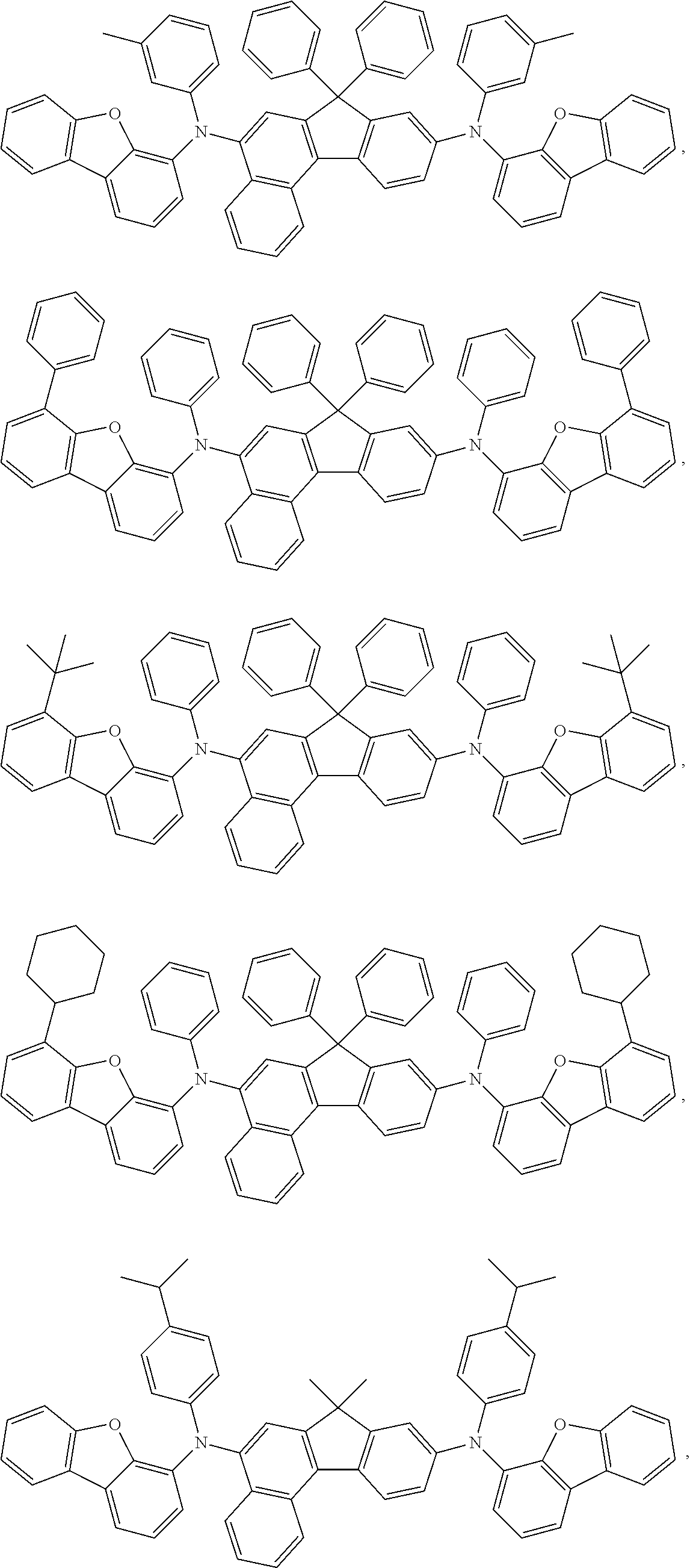
[0025] According to an embodiment of the present disclosure, a method of fabricating an organic light emitting device comprising a first electrode, a second electrode, and a first organic layer disposed between the first electrode and the second electrode, wherein the first organic layer comprises a first composition comprising a mixture of a first compound and a second compound is disclosed. The method comprising:
[0026] providing a substrate having the first electrode disposed thereon;
[0027] depositing the first organic layer over the first electrode; and
[0028] depositing the second electrode over the first organic layer, wherein the first compound has different chemical structure than the second compound;
[0029] wherein the mixture of the first compound and the second compound is capable of functioning as a delayed fluorescent emitter system in an organic light emitting device at room temperature;
[0030] wherein the first compound has an evaporation temperature T.sub.1 of 150 to 350.degree. C.;
[0031] wherein the second compound has an evaporation temperature T.sub.2 of 150 to 350.degree. C.;
[0032] wherein absolute value of T.sub.1-T.sub.2 is less than 20.degree. C.;
[0033] wherein the first compound has a concentration C.sub.1 in said mixture and a concentration C.sub.2 in a film formed by evaporating the mixture in a vacuum deposition tool at a constant pressure between 1.times.10.sup.-6 Torr to 1.times.10.sup.-9 Torr, at a 2 .ANG./sec deposition rate on a surface positioned at a predefined distance away from the mixture being evaporated; and
[0034] wherein absolute value of (C.sub.1-C.sub.2)/C.sub.1 is less than 5%.
BRIEF DESCRIPTION OF THE DRAWINGS
[0035] FIG. 1 shows an organic light emitting device that can incorporate the inventive materials system disclosed herein.
[0036] FIG. 2 shows an inverted organic light emitting device that can incorporate the inventive materials system disclosed herein.
DETAILED DESCRIPTION
[0037] Generally, an OLED comprises at least one organic layer disposed between and electrically connected to an anode and a cathode. When a current is applied, the anode injects holes and the cathode injects electrons into the organic layer(s). The injected holes and electrons each migrate toward the oppositely charged electrode. When an electron and hole localize on the same molecule, an "exciton," which is a localized electron-hole pair having an excited energy state, is formed. Light is emitted when the exciton relaxes via a photoemissive mechanism. In some cases, the exciton may be localized on an excimer or an exciplex. Non-radiative mechanisms, such as thermal relaxation, may also occur, but are generally considered undesirable.
[0038] The initial OLEDs used emissive molecules that emitted light from their singlet states ("fluorescence") as disclosed, for example, in U.S. Pat. No. 4,769,292, which is incorporated by reference in its entirety. Fluorescent emission generally occurs in a time frame of less than 10 nanoseconds.
[0039] More recently, OLEDs having emissive materials that emit light from triplet states ("phosphorescence") have been demonstrated. Baldo et al., "Highly Efficient Phosphorescent Emission from Organic Electroluminescent Devices," Nature, vol. 395, 151-154, 1998; ("Baldo-I") and Baldo et al., "Very high-efficiency green organic light-emitting devices based on electrophosphorescence," Appl. Phys. Lett., vol. 75, No. 3, 4-6 (1999) ("Baldo-II"), which are incorporated by reference in their entireties. Phosphorescence is described in more detail in U.S. Pat. No. 7,279,704 at cols. 5-6, which are incorporated by reference.
[0040] FIG. 1 shows an organic light emitting device 100. The figures are not necessarily drawn to scale. Device 100 may include a substrate 110, an anode 115, a hole injection layer 120, a hole transport layer 125, an electron blocking layer 130, an emissive layer 135, a hole blocking layer 140, an electron transport layer 145, an electron injection layer 150, a protective layer 155, a cathode 160, and a barrier layer 170. Cathode 160 is a compound cathode having a first conductive layer 162 and a second conductive layer 164. Device 100 may be fabricated by depositing the layers described, in order. The properties and functions of these various layers, as well as example materials, are described in more detail in U.S. Pat. No. 7,279,704 at cols. 6-10, which are incorporated by reference.
[0041] More examples for each of these layers are available. For example, a flexible and transparent substrate-anode combination is disclosed in U.S. Pat. No. 5,844,363, which is incorporated by reference in its entirety. An example of a p-doped hole transport layer is m-MTDATA doped with F.sub.4-TCNQ at a molar ratio of 50:1, as disclosed in U.S. Patent Application Publication No. 2003/0230980, which is incorporated by reference in its entirety. Examples of host materials are disclosed in U.S. Pat. No. 6,303,238 to Thompson et al., which is incorporated by reference in its entirety. An example of an n-doped electron transport layer is BPhen doped with Li at a molar ratio of 1:1, as disclosed in U.S. Patent Application Publication No. 2003/0230980, which is incorporated by reference in its entirety. U.S. Pat. Nos. 5,703,436 and 5,707,745, which are incorporated by reference in their entireties, disclose examples of cathodes including compound cathodes having a thin layer of metal such as Mg:Ag with an overlying transparent, electrically-conductive, sputter-deposited ITO layer. The theory and use of blocking layers is described in more detail in U.S. Pat. No. 6,097,147 and U.S. Patent Application Publication No. 2003/0230980, which are incorporated by reference in their entireties. Examples of injection layers are provided in U.S. Patent Application Publication No. 2004/0174116, which is incorporated by reference in its entirety. A description of protective layers may be found in U.S. Patent Application Publication No. 2004/0174116, which is incorporated by reference in its entirety.
[0042] FIG. 2 shows an inverted OLED 200. The device includes a substrate 210, a cathode 215, an emissive layer 220, a hole transport layer 225, and an anode 230. Device 200 may be fabricated by depositing the layers described, in order. Because the most common OLED configuration has a cathode disposed over the anode, and device 200 has cathode 215 disposed under anode 230, device 200 may be referred to as an "inverted" OLED. Materials similar to those described with respect to device 100 may be used in the corresponding layers of device 200. FIG. 2 provides one example of how some layers may be omitted from the structure of device 100.
[0043] The simple layered structure illustrated in FIGS. 1 and 2 is provided by way of non-limiting example, and it is understood that embodiments of the invention may be used in connection with a wide variety of other structures. The specific materials and structures described are exemplary in nature, and other materials and structures may be used. Functional OLEDs may be achieved by combining the various layers described in different ways, or layers may be omitted entirely, based on design, performance, and cost factors. Other layers not specifically described may also be included. Materials other than those specifically described may be used. Although many of the examples provided herein describe various layers as comprising a single material, it is understood that combinations of materials, such as a mixture of host and dopant, or more generally a mixture, may be used. Also, the layers may have various sublayers. The names given to the various layers herein are not intended to be strictly limiting. For example, in device 200, hole transport layer 225 transports holes and injects holes into emissive layer 220, and may be described as a hole transport layer or a hole injection layer. In one embodiment, an OLED may be described as having an "organic layer" disposed between a cathode and an anode. This organic layer may comprise a single layer, or may further comprise multiple layers of different organic materials as described, for example, with respect to FIGS. 1 and 2.
[0044] Structures and materials not specifically described may also be used, such as OLEDs comprised of polymeric materials (PLEDs) such as disclosed in U.S. Pat. No. 5,247,190 to Friend et al., which is incorporated by reference in its entirety. By way of further example, OLEDs having a single organic layer may be used. OLEDs may be stacked, for example as described in U.S. Pat. No. 5,707,745 to Forrest et al., which is incorporated by reference in its entirety. The OLED structure may deviate from the simple layered structure illustrated in FIGS. 1 and 2. For example, the substrate may include an angled reflective surface to improve out-coupling, such as a mesa structure as described in U.S. Pat. No. 6,091,195 to Forrest et al., and/or a pit structure as described in U.S. Pat. No. 5,834,893 to Bulovic et al., which are incorporated by reference in their entireties.
[0045] Unless otherwise specified, any of the layers of the various embodiments may be deposited by any suitable method. For the organic layers, preferred methods include thermal evaporation, ink-jet, such as described in U.S. Pat. Nos. 6,013,982 and 6,087,196, which are incorporated by reference in their entireties, organic vapor phase deposition (OVPD), such as described in U.S. Pat. No. 6,337,102 to Forrest et al., which is incorporated by reference in its entirety, and deposition by organic vapor jet printing (OVJP), such as described in U.S. Pat. No. 7,431,968, which is incorporated by reference in its entirety. Other suitable deposition methods include spin coating and other solution based processes. Solution based processes are preferably carried out in nitrogen or an inert atmosphere. For the other layers, preferred methods include thermal evaporation. Preferred patterning methods include deposition through a mask, cold welding such as described in U.S. Pat. Nos. 6,294,398 and 6,468,819, which are incorporated by reference in their entireties, and patterning associated with some of the deposition methods such as ink-jet and OVJD. Other methods may also be used. The materials to be deposited may be modified to make them compatible with a particular deposition method. For example, substituents such as alkyl and aryl groups, branched or unbranched, and preferably containing at least 3 carbons, may be used in small molecules to enhance their ability to undergo solution processing. Substituents having 20 carbons or more may be used, and 3-20 carbons is a preferred range. Materials with asymmetric structures may have better solution processibility than those having symmetric structures, because asymmetric materials may have a lower tendency to recrystallize. Dendrimer substituents may be used to enhance the ability of small molecules to undergo solution processing.
[0046] Devices fabricated in accordance with embodiments of the present invention may further optionally comprise a barrier layer. One purpose of the barrier layer is to protect the electrodes and organic layers from damaging exposure to harmful species in the environment including moisture, vapor and/or gases, etc. The barrier layer may be deposited over, under or next to a substrate, an electrode, or over any other parts of a device including an edge. The barrier layer may comprise a single layer, or multiple layers. The barrier layer may be formed by various known chemical vapor deposition techniques and may include compositions having a single phase as well as compositions having multiple phases. Any suitable material or combination of materials may be used for the barrier layer. The barrier layer may incorporate an inorganic or an organic compound or both. The preferred barrier layer comprises a mixture of a polymeric material and a non-polymeric material as described in U.S. Pat. No. 7,968,146, PCT Pat. Application Nos. PCT/US2007/023098 and PCT/US2009/042829, which are herein incorporated by reference in their entireties. To be considered a "mixture", the aforesaid polymeric and non-polymeric materials comprising the barrier layer should be deposited under the same reaction conditions and/or at the same time. The weight ratio of polymeric to non-polymeric material may be in the range of 95:5 to 5:95. The polymeric material and the non-polymeric material may be created from the same precursor material. In one example, the mixture of a polymeric material and a non-polymeric material consists essentially of polymeric silicon and inorganic silicon.
[0047] Devices fabricated in accordance with embodiments of the invention may be incorporated into a wide variety of consumer products, including flat panel displays, computer monitors, medical monitors, televisions, billboards, lights for interior or exterior illumination and/or signaling, heads up displays, fully transparent displays, flexible displays, laser printers, telephones, cell phones, personal digital assistants (PDAs), laptop computers, digital cameras, camcorders, viewfinders, micro-displays, 3-D displays, vehicles, a large area wall, theater or stadium screen, or a sign. Various control mechanisms may be used to control devices fabricated in accordance with the present invention, including passive matrix and active matrix. Many of the devices are intended for use in a temperature range comfortable to humans, such as 18 degrees C. to 30 degrees C., and more preferably at room temperature (20-25 degrees C.), but could be used outside this temperature range, for example, from -40 degree C. to +80 degree C.
[0048] The materials and structures described herein may have applications in devices other than OLEDs. For example, other optoelectronic devices such as organic solar cells and organic photodetectors may employ the materials and structures. More generally, organic devices, such as organic transistors, may employ the materials and structures.
[0049] The term "halo" or "halogen" as used herein includes fluorine, chlorine, bromine, and iodine.
[0050] The term "alkyl" as used herein contemplates both straight and branched chain alkyl radicals. Preferred alkyl groups are those containing from one to fifteen carbon atoms and includes methyl, ethyl, propyl, isopropyl, butyl, isobutyl, tert-butyl, and the like. Additionally, the alkyl group may be optionally substituted.
[0051] The term "cycloalkyl" as used herein contemplates cyclic alkyl radicals. Preferred cycloalkyl groups are those containing 3 to 7 carbon atoms and includes cyclopropyl, cyclopentyl, cyclohexyl, and the like. Additionally, the cycloalkyl group may be optionally substituted.
[0052] The term "alkenyl" as used herein contemplates both straight and branched chain alkene radicals. Preferred alkenyl groups are those containing two to fifteen carbon atoms. Additionally, the alkenyl group may be optionally substituted.
[0053] The term "alkynyl" as used herein contemplates both straight and branched chain alkyne radicals. Preferred alkyl groups are those containing two to fifteen carbon atoms. Additionally, the alkynyl group may be optionally substituted.
[0054] The terms "aralkyl" or "arylalkyl" as used herein are used interchangeably and contemplate an alkyl group that has as a substituent an aromatic group. Additionally, the aralkyl group may be optionally substituted.
[0055] The term "heterocyclic group" as used herein contemplates aromatic and non-aromatic cyclic radicals. Hetero-aromatic cyclic radicals also refer to heteroaryl. Preferred hetero-non-aromatic cyclic groups are those containing 3 or 7 ring atoms which includes at least one hetero atom, and includes cyclic amines such as morpholino, piperdino, pyrrolidino, and the like, and cyclic ethers, such as tetrahydrofuran, tetrahydropyran, and the like. Additionally, the heterocyclic group may be optionally substituted.
[0056] The term "aryl" or "aromatic group" as used herein contemplates single-ring groups and polycyclic ring systems. The polycyclic rings may have two or more rings in which two carbons are common to two adjoining rings (the rings are "fused") wherein at least one of the rings is aromatic, e.g., the other rings can be cycloalkyls, cycloalkenyls, aryl, heterocycles, and/or heteroaryls. Additionally, the aryl group may be optionally substituted.
[0057] The term "heteroaryl" as used herein contemplates single-ring hetero-aromatic groups that may include from one to three heteroatoms, for example, pyrrole, furan, thiophene, imidazole, oxazole, thiazole, triazole, pyrazole, pyridine, pyrazine and pyrimidine, and the like. The term heteroaryl also includes polycyclic hetero-aromatic systems having two or more rings in which two atoms are common to two adjoining rings (the rings are "fused") wherein at least one of the rings is a heteroaryl, e.g., the other rings can be cycloalkyls, cycloalkenyls, aryl, heterocycles, and/or heteroaryls. Additionally, the heteroaryl group may be optionally substituted.
[0058] The alkyl, cycloalkyl, alkenyl, alkynyl, aralkyl, heterocyclic group, aryl, and heteroaryl may be optionally substituted with one or more substituents selected from the group consisting of hydrogen, deuterium, halogen, alkyl, cycloalkyl, heteroalkyl, arylalkyl, alkoxy, aryloxy, amino, cyclic amino, silyl, alkenyl, cycloalkenyl, heteroalkenyl, alkynyl, aryl, heteroaryl, acyl, carbonyl, carboxylic acid, ether, ester, nitrile, isonitrile, sulfanyl, sulfinyl, sulfonyl, phosphino, and combinations thereof.
[0059] As used herein, "substituted" indicates that a substituent other than H is bonded to the relevant position, such as carbon. Thus, for example, where R.sup.1 is mono-substituted, then one R.sup.1 must be other than H. Similarly, where R.sup.1 is di-substituted, then two of R.sup.1 must be other than H. Similarly, where R.sup.1 is unsubstituted, R.sup.1 is hydrogen for all available positions.
[0060] The "aza" designation in the fragments described herein, i.e. aza-dibenzofuran, aza-dibenzonethiophene, etc. means that one or more of the C--H groups in the respective fragment can be replaced by a nitrogen atom, for example, and without any limitation, azatriphenylene encompasses both dibenzo[f,h]quinoxaline and dibenzo[f,h]quinoline. One of ordinary skill in the art can readily envision other nitrogen analogs of the aza-derivatives described above, and all such analogs are intended to be encompassed by the terms as set forth herein.
[0061] It is to be understood that when a molecular fragment is described as being a substituent or otherwise attached to another moiety, its name may be written as if it were a fragment (e.g. naphthyl, dibenzofuryl) or as if it were the whole molecule (e.g. naphthalene, dibenzofuran). As used herein, these different ways of designating a substituent or attached fragment are considered to be equivalent.
[0062] Often, the emissive layer (EML) of OLED devices exhibiting good lifetime and efficiency requires more than two components (e.g. 3 or 4 components). Fabricating such EMLs using vacuum thermal evaporation (VTE) process then requires evaporating 3 or 4 evaporation source materials in separate VTE sublimation crucibles, which is very complicated and costly compared to a standard two-component EML with a single host and an emitter, which requires only two evaporation sources.
[0063] Premixing two or more materials and evaporating them from one VTE sublimation crucible can reduce the complexity of the fabrication process. However, the co-evaporation must be stable and produce an evaporated film having a composition that remains constant through the evaporation process. Variations in the film's composition may adversely affect the device performance. In order to obtain a stable co-evaporation from a mixture of compounds under vacuum, one would assume that the materials must have the same evaporation temperature under the same condition. However, this may not be the only parameter one has to consider. When two compounds are mixed together, they may interact with each other and the evaporation property of the mixture may differ from their individual properties. On the other hand, materials with slightly different evaporation temperatures may form a stable co-evaporation mixture. Therefore, it is extremely difficult to achieve a stable co-evaporation mixture. So far, there have been very few stable co-evaporation mixture examples. "Evaporation temperature" of a material is measured in a vacuum deposition tool at a constant pressure, normally between 1.times.10.sup.-7 Torr to 1.times.10.sup.-8 Torr, at a 2 .ANG./sec deposition rate on a surface positioned at a set distance away from the evaporation source of the material being evaporated, e.g. sublimation crucible in a VTE tool. The various measured values such as temperature, pressure, deposition rate, etc. disclosed herein are expected to have nominal variations because of the expected tolerances in the measurements that produced these quantitative values as understood by one of ordinary skill in the art.
[0064] Many factors other than temperature can contribute to the ability to achieve stable co-evaporation, such as the miscibility of the different materials and the phase transition temperatures of the different materials. The inventors found that when two materials have similar evaporation temperatures, and similar mass loss rate or similar vapor pressures, the two materials can co-evaporate consistently. "Mass loss rate" of a material is defined as the percentage of mass lost over time ("percentage/minute" or "%/min") and is determined by measuring the time it takes to lose the first 10% of the mass of a sample of the material as measured by thermal gravity analysis (TGA) under a given experimental condition at a given constant temperature for a given material after the a steady evaporation state is reached. The given constant temperature is one temperature point that is chosen so that the value of mass loss rate is between about 0.05 to 0.50%/min. A skilled person in this field should appreciate that in order to compare two parameters, the experimental condition should be consistent. The method of measuring mass loss rate and vapor pressure is well known in the art and can be found, for example, in Bull. et al. Mater. Sci. 2011, 34, 7.
[0065] In the state of the art OLED devices, the EML may consist of three or more components. In one example, the EML can consist of two host-type compounds and an emitter combination (e.g. a hole transporting cohost (h-host), an electron transporting cohost (e-host), and a compound capable of functioning as an emitter in an OLED at room temperature). In another example, the EML can consist of one host-type compound and two emitter-type compounds (e.g., a host compound and two compounds each capable of functioning as an emitter in an OLED at room temperature). Conventionally, in order to fabricate such EMLs having three or more components using VTE process, three or more evaporation sources are required, one for each of the components. Because the concentration of the components are important for the device performance, typically, the rate of deposition of each component is measured individually during the deposition process. This makes the VTE process complicated and costly. Thus, it is desired to premix at least two of the components of such EMLs to reduce the number of VTE evaporation sources.
[0066] As used herein, an "emitter-type compound" refers to a compound that is capable of functioning as an emitter in the EML of an OLED at room temperature. A "host-type compound" refers to a compound that is capable of functioning as a host material in the EML of an OLED at room temperature.
[0067] If any two of the three or more components of the EMLs can be premixed and form a stable mixture of co-evaporation source, then the number of evaporation sources required for EML layer fabrication would be reduced. In order for materials to be premixable into an evaporation source, they should co-evaporate and deposit uniformly without changing the ratio. The ratio of the components in the mixture should be the same as the ratio of the components in the evaporation deposited films from these premixed materials. Therefore, the concentration of the two components in the deposited film is controlled by their concentration in the premixed evaporation source.
[0068] The present disclosure describes premixed materials with P-type or E-type delayed fluorescent systems in the device. It is believed that the internal quantum efficiency (IQE) of fluorescent OLEDs can exceed the 25% spin statistics limit through delayed fluorescence. As used herein, there are two types of delayed fluorescence, i.e. P-type delayed fluorescence and E-type delayed fluorescence.
[0069] P-type delayed fluorescence is generated from triplet-triplet annihilation (TTA). P-type delayed fluorescence characteristics can be found in a host-emitter system or in a single compound. Without being bound by theory, it is believed that in a host-emitter delayed fluorescent system, TTA can be generated in the host, and then transferred to emitter.
[0070] On the other hand, E-type delayed fluorescence does not rely on the collision of two triplets, but rather on the thermal population between the triplet states and the singlet excited states. Compounds that are capable of generating E-type delayed fluorescence are required to have very small singlet-triplet gaps. Thermal energy can activate the transition from the triplet state back to the singlet state. This type of delayed fluorescence is also known as thermally activated delayed fluorescence (TADF). A distinctive feature of TADF is that the delayed component increases as temperature rises due to the increased thermal energy. If the reverse intersystem crossing rate is fast enough to minimize the non-radiative decay from the triplet state, the fraction of back populated singlet excited states can potentially reach 75%. The total singlet fraction can be 100%, far exceeding the spin statistics limit for electrically generated excitons.
[0071] E-type delayed fluorescence characteristics can be found in an exciplex system or in a single compound. Without being bound by theory, it is believed that E-type delayed fluorescence requires the luminescent material to have a small singlet-triplet energy gap (.DELTA.E.sub.S-T). Organic, non-metal containing, donor-acceptor luminescent materials may be able to achieve this. The emission in these materials is often characterized as a donor-acceptor charge-transfer (CT) type emission. The spatial separation of the HOMO and LUMO in these donor-acceptor type compounds often results in small .DELTA.E.sub.S-T. These states may involve CT states. Often, donor-acceptor luminescent materials are constructed by connecting an electron donor moiety such as amino- or carbazole-derivatives and an electron acceptor moiety such as N-containing six-membered aromatic rings.
[0072] According to the present disclosure, a composition comprising a mixture of a first compound with a different chemical structure than a second compound is disclosed. The mixture of the first compound and the second compound is capable of functioning as a delayed fluorescent system in an organic light emitting device at room temperature. In some embodiments, the first compound has an evaporation temperature T.sub.1 of 150 to 350.degree. C., the second compound has an evaporation temperature T.sub.2 of 150 to 350.degree. C., and the absolute value of T.sub.1-T.sub.2 is less than 20.degree. C. In some embodiments, the first compound has evaporation temperature T.sub.1 of 200 to 350.degree. C. and the second compound has evaporation temperature T.sub.2 of 200 to 350.degree. C.
[0073] In some embodiments, the first compound has a concentration C.sub.1 in the mixture and a concentration C.sub.2 in a film formed by evaporating the mixture in a vacuum deposition tool at a constant pressure between 1.times.10.sup.-6 Torr to 1.times.10.sup.-9 Torr, at a 2 .ANG./sec deposition rate on a surface positioned at a predefined distance away from the mixture being evaporated. In some embodiments, the absolute value of (C.sub.1-C.sub.2)/C.sub.1 is less than 5%. In some embodiments, the absolute value of (C.sub.1-C.sub.2)/C.sub.1 is less than 4%, or less that 3%, or less than 2%, or less than 1%.
[0074] The first compound can have a vapor pressure of P.sub.1 at T.sub.1 at 1 atm, and the second compound can have a vapor pressure of P.sub.2 at T.sub.2 at 1 atm. In some embodiments, the ratio of P.sub.1/P.sub.2 is within the range of 0.90:1 to 1.10:1. In some embodiments, the ratio of P.sub.1/P.sub.2 is within the range of 0.95:1 to 1.05:1. In some embodiments, the ratio of P.sub.1/P.sub.2 is within the range of 0.97:1 to 1.03:1.
[0075] The first compound has a first mass loss rate and the second compound has a second mass loss rate. In some embodiments, the ratio between the first mass loss rate and the second mass loss rate is within the range of 0.90:1 to 1.10:1. In some embodiments, the ratio between the first mass loss rate and the second mass loss rate is within the range of 0.95:1 to 1.05:1. In some embodiments, the ratio between the first mass loss rate and the second mass loss rate is within the range of 0.97 to 1.03.
[0076] In some embodiments, the second compound is capable of functioning as a host in an organic light emitting device at room temperature. In some embodiments, the host is a hole transporting host. In some embodiments, the host is an electron transporting host.
[0077] In some embodiments, the second compound comprises at least one chemical group selected from the group consisting of anthracence, naphthylene, phenanthrene, triphenylene, carbazole, dibenzothiphene, dibenzofuran, dibenzoselenophene, aza-triphenylene, aza-carbazole, aza-dibenzothiophene, aza-dibenzofuran, and aza-dibenzoselenophen.
[0078] In some embodiments, the the first compound and the second compound each has a purity in excess of 99% as determined by high pressure liquid chromatography.
[0079] In some embodiments, the composition further comprises a third compound. In such embodiments, the third compound has a different chemical structure than the first and second compounds, the third compound has an evaporation temperature T.sub.3 of 150 to 350.degree. C. In some such embodiments, the absolute value of T.sub.1-T.sub.3 is less than 20.degree. C.
[0080] In some embodiments, the composition is in liquid form at a temperature less than the lesser of T.sub.1 and T.sub.2.
[0081] In some embodiments, the delayed fluorescent system is a P-type delayed fluorescent system. In some such embodiments, the first compound comprises at least one chemical group selected from the group consisting of pyrene, fluoranthene, chrysene, benzofluorene, and stilbene.
[0082] In some embodiments, the delayed fluorescent system is a P-type delayed fluorescent system, and the first compound is an emitter selected from the group consisting of:
##STR00002## ##STR00003## ##STR00004## ##STR00005## ##STR00006## ##STR00007## ##STR00008## ##STR00009## ##STR00010## ##STR00011## ##STR00012## ##STR00013## ##STR00014## ##STR00015## ##STR00016## ##STR00017## ##STR00018## ##STR00019## ##STR00020## ##STR00021## ##STR00022## ##STR00023## ##STR00024## ##STR00025## ##STR00026## ##STR00027## ##STR00028## ##STR00029## ##STR00030## ##STR00031## ##STR00032## ##STR00033## ##STR00034##
Additional examples of emitters for use in P-type delayed fluorescent systems such as those described herein include, but are not limited, to those compounds disclosed in the following patents and patent applications: WO2010027181A2; U.S. Pat. Nos. 7,488,856; 7,488,856; 7,919,197; 8,628,863; US2010117526; US2010127618; US2012013700; WO2010047403; WO2010067893; WO2014024687; JP2011037838; WO08091130; US2008306303; EP2161319; EP2182038; CN102232068; EP01604974; EP01860097; EP02008992; EP1860096; EP2085371; EP2159217; EP2700696; JP2008-069128; JP2013087090; US20060210830; US20070236137; US20080015399; US20090058284; U.S. Ser. No. 07/425,653; U.S. Pat. No. 7,705,183; US2009195149; US2012013244; US2014183500; US20110006289; WO2009102054; WO2010013675; WO2010018842; WO2010018843; WO2010122810; WO2011077689; WO2013042769; WO2013077385; WO2013077405; WO2014069602; EP01437395A2; WO07108666; US20090134781; US2004137270; WO06122630; WO2014111269; EP01818322; U.S. Pat. Nos. 8,623,521; 8,771,844; US2014183468; US20130234118; KR0117694; and US2008203905, the entireties of which are incorporated herein by reference.
[0083] In some embodiments, the delayed fluorescent system is a P-type delayed fluorescent system, and the second compound is a host selected from the group consisting of:
##STR00035## ##STR00036## ##STR00037## ##STR00038## ##STR00039## ##STR00040## ##STR00041## ##STR00042## ##STR00043## ##STR00044## ##STR00045## ##STR00046## ##STR00047## ##STR00048## ##STR00049## ##STR00050## ##STR00051## ##STR00052## ##STR00053## ##STR00054## ##STR00055## ##STR00056## ##STR00057## ##STR00058## ##STR00059## ##STR00060## ##STR00061## ##STR00062## ##STR00063## ##STR00064## ##STR00065## ##STR00066## ##STR00067## ##STR00068## ##STR00069## ##STR00070## ##STR00071##
Additional examples of hosts for use in P-type delayed fluorescent emitter systems such as those described herein include, but are not limited, to those compounds disclosed in the following patents and patent applications: US20070173658; WO2010071362; WO2011037380; EP2147962; WO2009066809; WO2012147568; EP01696015; EP01775783; EP2163550; US20080111473; US20080193799; US2014008641; WO07114358; WO2009063846; WO2009066641; WO2014034869; WO2014034891; US20050211958; US20050245752; U.S. Pat. No. 6,465,115; WO07086695; EP01972619; KR20090086015; US20140246657; and US20090169921, the entireties of which are incorporated herein by reference.
[0084] In some embodiments, the delayed fluorescent emitter system is an E-type delayed fluorescent emitter system. In some embodiments, the first compound has the formula of D-L-A, where D is an electron donor group, A is an electron acceptor group, and L is a direct bond or linker.
[0085] In some embodiments, the electron donor group (D) comprises at least one chemical group selected from the group consisting of amino, indole, carbazole, benzothiohpene, benzofuran, benzoselenophene, dibenzothiophene, dibenzofuran, dibenzoselenophene, and combinations thereof. In some embodiments, the electron donor group (D) comprises at least one chemical group selected from the group consisting of:
##STR00072## ##STR00073##
[0086] where: n is an integer from 1 to 20; m is an integer from 1 to 20; X and Y are independently selected from the group consisting of O, S, and NR.sup.14; and R.sup.11, R.sup.12, R.sup.13 and R.sup.14 are selected from the group consisting of aryl and heteroaryl.
[0087] In some embodiments, the electron acceptor group (A) includes a structure selected from the group consisting of:
##STR00074##
In some embodiments, the electron acceptor group (A) includes the structure
##STR00075##
where Z.sup.1, Z.sup.2, Z.sup.3, Z.sup.4, Z.sup.5, Z.sup.6, Z.sup.7, and Z.sup.8 each independently comprise C or N; and at least two of Z.sup.1, Z.sup.2, Z.sup.3, Z.sup.4, Z.sup.5, Z.sup.6, Z.sup.7, and Z.sup.8 are N. In some embodiments, exactly two of Z.sup.1, Z.sup.2, Z.sup.3, Z.sup.4, Z.sup.5, Z.sup.6, Z.sup.7, and Z.sup.8 are N. In some embodiments, the electron acceptor group (A) described above are further substituted.
[0088] In some embodiments, the electron acceptor group (A) includes at least one chemical group selected from the group consisting of:
##STR00076##
where Y.sup.1 to Y.sup.8 independently comprise C or N; A.sup.1 to A.sup.8 independently comprise C or N; J.sup.1 and J.sup.2 independently comprise C or N; L.sup.1 to L.sup.4 independently comprise C or N; X.sup.1 is O, S, or NR.sup.14; and R.sup.14 is aryl or heteroaryl. In some embodiments, the electron acceptor group (A) is further substituted.
[0089] In some more specific embodiments, the donor group (D) is selected from the group consisting
of
##STR00077## ##STR00078## ##STR00079## ##STR00080## ##STR00081## ##STR00082## ##STR00083## ##STR00084## ##STR00085## ##STR00086## ##STR00087## ##STR00088## ##STR00089##
[0090] In some embodiments, the acceptor group (A) is selected from the group consisting of:
##STR00090## ##STR00091## ##STR00092## ##STR00093## ##STR00094## ##STR00095## ##STR00096##
[0091] In some embodiments, the delayed fluorscence system is an E-type delayed fluorescent system. In some such embodiments, the first compound is an emitter selected from the group consisting of:
##STR00097## ##STR00098## ##STR00099## ##STR00100## ##STR00101## ##STR00102## ##STR00103## ##STR00104## ##STR00105## ##STR00106## ##STR00107## ##STR00108## ##STR00109## ##STR00110## ##STR00111## ##STR00112## ##STR00113## ##STR00114## ##STR00115## ##STR00116## ##STR00117## ##STR00118## ##STR00119## ##STR00120## ##STR00121## ##STR00122## ##STR00123## ##STR00124## ##STR00125## ##STR00126##
Additional examples of emitters for use in E-type delayed fluorescent systems such as those described herein include, but are not limited, to those compounds disclosed in the following patents and patent applications: WO2013154064; WO2014104315; US2014145151; US2014145149; US2014158992; US2014138627; and US2014131665, the entireties of which are incorporated herein by reference.
[0092] In some embodiments, the delayed fluorescent system is an E-type delayed fluorescent system and the the second compound is a host selected from the group consisting of:
##STR00127## ##STR00128## ##STR00129## ##STR00130## ##STR00131## ##STR00132## ##STR00133## ##STR00134## ##STR00135##
Additional examples of hosts for use in E-type delayed fluorescent systems such as those described herein include, but are not limited, to those compounds disclosed in the following patents and patent applications: WO2001039234; US20060280965; WO2008056746; WO2010107244; US20100187984; US20090167162; WO2009086028; US20090017330; US20100084966; US20050238919; EP2034538; US20140183503; WO2013081315; WO2014142472; WO2013191404; US20140225088; EP2757608; US2013105787; KR20100079458; KR20120088644; WO2014030872; US2014034914; US2012126221; US2014001446; KR20130115564; KR20120129733; US2013175519; TW201329200; WO2012133644; WO2011081431; WO2013035275; US2013009543; WO2013024872; US2012075273; WO2012133649; WO2011081423; WO2012128298; and US2010187984, the entireties of which are incorporated herein by reference.
[0093] According to another aspect of the present disclosure, a device that includes one or more organic light emitting devices is also provided. The one or more organic light emitting devices can include an anode, a cathode, and an emissive layer disposed between the anode and the cathode. The emissive layer can include a delayed fluorescence composition including a first compound and a second compound as described herein. In some embodiments, the first device emits a luminescent radiation at room temperature when a voltage is applied across the organic light emitting device, and the luminescent radiation comprises a delayed fluorescence process. In some embodiments, the first device emits a white light.
[0094] In some embodiments, the emissive layer further comprises a first phosphorescent emitting material. In some embodiments, the emissive layer further comprises a second phosphorescent emitting material.
[0095] In some embodiments, the device comprises a second organic light emitting device, and the second organic light emitting device is stacked on the first organic light emitting device. In some embodiments, the device is selected from the group consisting of a consumer product, an electronic component module, an organic light emitting device, and a lighting panel.
[0096] According to another aspect of the present disclosure, a method for fabricating an organic light emitting device comprising a first electrode, a second electrode, and a first organic layer disposed between the first electrode and the second electrode is described. The first organic layer can include a delayed fluorescence composition including a first compound and a second compound as described herein. The method can include providing a substrate having the first electrode disposed thereon; depositing a first organic layer over the first electrode; and depositing the second electrode over the first organic layer, where the first organic layer includes a delayed fluorescence composition including a first compound and a second compound as described herein.
Combination with Other Materials
[0097] The materials described herein as useful for a particular layer in an organic light emitting device may be used in combination with a wide variety of other materials present in the device. For example, emissive dopants disclosed herein may be used in conjunction with a wide variety of hosts, transport layers, blocking layers, injection layers, electrodes and other layers that may be present. The materials described or referred to below are non-limiting examples of materials that may be useful in combination with the compounds disclosed herein, and one of skill in the art can readily consult the literature to identify other materials that may be useful in combination.
HIL/HTL:
[0098] A hole injecting/transporting material to be used in the present invention is not particularly limited, and any compound may be used as long as the compound is typically used as a hole injecting/transporting material. Examples of the material include, but are not limited to: a phthalocyanine or porphyrin derivative; an aromatic amine derivative; an indolocarbazole derivative; a polymer containing fluorohydrocarbon; a polymer with conductivity dopants; a conducting polymer, such as PEDOT/PSS; a self-assembly monomer derived from compounds such as phosphonic acid and silane derivatives; a metal oxide derivative, such as MoO.sub.x; a P-type semiconducting organic compound, such as 1,4,5,8,9,12-Hexaazatriphenylenehexacarbonitrile; a metal complex, and a cross-linkable compounds.
[0099] Examples of aromatic amine derivatives used in HIL or HTL include, but are not limited to, the following general structures:
##STR00136##
[0100] Each of Ar.sup.1 to Ar.sup.9 is selected from the group consisting of aromatic hydrocarbon cyclic compounds such as benzene, biphenyl, triphenyl, triphenylene, naphthalene, anthracene, phenalene, phenanthrene, fluorene, pyrene, chrysene, perylene, and azulene; the group consisting of aromatic heterocyclic compounds such as dibenzothiophene, dibenzofuran, dibenzoselenophene, furan, thiophene, benzofuran, benzothiophene, benzoselenophene, carbazole, indolocarbazole, pyridylindole, pyrrolodipyridine, pyrazole, imidazole, triazole, oxazole, thiazole, oxadiazole, oxatriazole, dioxazole, thiadiazole, pyridine, pyridazine, pyrimidine, pyrazine, triazine, oxazine, oxathiazine, oxadiazine, indole, benzimidazole, indazole, indoxazine, benzoxazole, benzisoxazole, benzothiazole, quinoline, isoquinoline, cinnoline, quinazoline, quinoxaline, naphthyridine, phthalazine, pteridine, xanthene, acridine, phenazine, phenothiazine, phenoxazine, benzofuropyridine, furodipyridine, benzothienopyridine, thienodipyridine, benzoselenophenopyridine, and selenophenodipyridine; and the group consisting of 2 to 10 cyclic structural units which are groups of the same type or different types selected from the aromatic hydrocarbon cyclic group and the aromatic heterocyclic group and are bonded to each other directly or via at least one of oxygen atom, nitrogen atom, sulfur atom, silicon atom, phosphorus atom, boron atom, chain structural unit and the aliphatic cyclic group. Wherein each Ar is further substituted by a substituent selected from the group consisting of hydrogen, deuterium, halide, alkyl, cycloalkyl, heteroalkyl, arylalkyl, alkoxy, aryloxy, amino, silyl, alkenyl, cycloalkenyl, heteroalkenyl, alkynyl, aryl, heteroaryl, acyl, carbonyl, carboxylic acids, ester, nitrile, isonitrile, sulfanyl, sulfinyl, sulfonyl, phosphino, and combinations thereof.
[0101] In one aspect, Ar.sup.1 to Ar.sup.9 is independently selected from the group consisting of:
##STR00137##
wherein k is an integer from 1 to 20; X.sup.101 to X.sup.108 is C (including CH) or N; Z.sup.101 is NAr.sup.1, O, or S; Ar.sup.1 has the same group defined above.
[0102] Examples of metal complexes used in HIL or HTL include, but are not limited to, the following general formula:
##STR00138##
wherein Met is a metal, which can have an atomic weight greater than 40; (Y.sup.101-Y.sup.102) is a bidentate ligand, Y.sup.101 and Y.sup.102 are independently selected from C, N, O, P, and S; L.sup.101 is an ancillary ligand; k' is an integer value from 1 to the maximum number of ligands that may be attached to the metal; and k'+k'' is the maximum number of ligands that may be attached to the metal.
[0103] In one aspect, (Y.sup.101-Y.sup.102) is a 2-phenylpyridine derivative. In another aspect, (Y.sup.101-Y.sup.102) is a carbene ligand. In another aspect, Met is selected from Ir, Pt, Os, and Zn. In a further aspect, the metal complex has a smallest oxidation potential in solution vs. Fc.sup.+/Fc couple less than about 0.6 V.
Host:
[0104] The light emitting layer of the organic EL device of the present invention preferably contains at least a metal complex as light emitting material, and may contain a host material using the metal complex as a dopant material. Examples of the host material are not particularly limited, and any metal complexes or organic compounds may be used as long as the triplet energy of the host is larger than that of the dopant. While the Table below categorizes host materials as preferred for devices that emit various colors, any host material may be used with any dopant so long as the triplet criteria is satisfied.
[0105] Examples of metal complexes used as host are preferred to have the following general formula:
##STR00139##
wherein Met is a metal; (Y.sup.103-Y.sup.104) is a bidentate ligand, Y.sup.103 and Y.sup.104 are independently selected from C, N, O, P, and S; L.sup.101 is an another ligand; k' is an integer value from 1 to the maximum number of ligands that may be attached to the metal; and k'+k'' is the maximum number of ligands that may be attached to the metal.
[0106] In one aspect, the metal complexes are:
##STR00140##
wherein (O--N) is a bidentate ligand, having metal coordinated to atoms O and N.
[0107] In another aspect, Met is selected from Ir and Pt. In a further aspect, (Y.sup.103-Y.sup.104) is a carbene ligand.
[0108] Examples of organic compounds used as host are selected from the group consisting of aromatic hydrocarbon cyclic compounds such as benzene, biphenyl, triphenyl, triphenylene, naphthalene, anthracene, phenalene, phenanthrene, fluorene, pyrene, chrysene, perylene, and azulene; the group consisting of aromatic heterocyclic compounds such as dibenzothiophene, dibenzofuran, dibenzoselenophene, furan, thiophene, benzofuran, benzothiophene, benzoselenophene, carbazole, indolocarbazole, pyridylindole, pyrrolodipyridine, pyrazole, imidazole, triazole, oxazole, thiazole, oxadiazole, oxatriazole, dioxazole, thiadiazole, pyridine, pyridazine, pyrimidine, pyrazine, triazine, oxazine, oxathiazine, oxadiazine, indole, benzimidazole, indazole, indoxazine, benzoxazole, benzisoxazole, benzothiazole, quinoline, isoquinoline, cinnoline, quinazoline, quinoxaline, naphthyridine, phthalazine, pteridine, xanthene, acridine, phenazine, phenothiazine, phenoxazine, benzofuropyridine, furodipyridine, benzothienopyridine, thienodipyridine, benzoselenophenopyridine, and selenophenodipyridine; and the group consisting of 2 to 10 cyclic structural units which are groups of the same type or different types selected from the aromatic hydrocarbon cyclic group and the aromatic heterocyclic group and are bonded to each other directly or via at least one of oxygen atom, nitrogen atom, sulfur atom, silicon atom, phosphorus atom, boron atom, chain structural unit and the aliphatic cyclic group. Wherein each group is further substituted by a substituent selected from the group consisting of hydrogen, deuterium, halide, alkyl, cycloalkyl, heteroalkyl, arylalkyl, alkoxy, aryloxy, amino, silyl, alkenyl, cycloalkenyl, heteroalkenyl, alkynyl, aryl, heteroaryl, acyl, carbonyl, carboxylic acids, ester, nitrile, isonitrile, sulfanyl, sulfinyl, sulfonyl, phosphino, and combinations thereof.
[0109] In one aspect, the host compound contains at least one of the following groups in the molecule:
##STR00141## ##STR00142##
wherein R.sup.101 to R.sup.107 is independently selected from the group consisting of hydrogen, deuterium, halide, alkyl, cycloalkyl, heteroalkyl, arylalkyl, alkoxy, aryloxy, amino, silyl, alkenyl, cycloalkenyl, heteroalkenyl, alkynyl, aryl, heteroaryl, acyl, carbonyl, carboxylic acids, ester, nitrile, isonitrile, sulfanyl, sulfinyl, sulfonyl, phosphino, and combinations thereof, when it is aryl or heteroaryl, it has the similar definition as Ar's mentioned above. k is an integer from 0 to 20 or 1 to 20; k''' is an integer from 0 to 20. X.sup.101 to X.sup.108 is selected from C (including CH) or N. Z.sup.101 and Z.sup.102 is selected from NR.sup.101, O, or S.
HBL:
[0110] A hole blocking layer (HBL) may be used to reduce the number of holes and/or excitons that leave the emissive layer. The presence of such a blocking layer in a device may result in substantially higher efficiencies as compared to a similar device lacking a blocking layer. Also, a blocking layer may be used to confine emission to a desired region of an OLED.
[0111] In one aspect, compound used in HBL contains the same molecule or the same functional groups used as host described above.
[0112] In another aspect, compound used in HBL contains at least one of the following groups in the molecule:
##STR00143##
wherein k is an integer from 1 to 20; L.sup.101 is an another ligand, k' is an integer from 1 to 3.
ETL:
[0113] Electron transport layer (ETL) may include a material capable of transporting electrons. Electron transport layer may be intrinsic (undoped), or doped. Doping may be used to enhance conductivity. Examples of the ETL material are not particularly limited, and any metal complexes or organic compounds may be used as long as they are typically used to transport electrons.
[0114] In one aspect, compound used in ETL contains at least one of the following groups in the molecule:
##STR00144##
wherein R.sup.101 is selected from the group consisting of hydrogen, deuterium, halide, alkyl, cycloalkyl, heteroalkyl, arylalkyl, alkoxy, aryloxy, amino, silyl, alkenyl, cycloalkenyl, heteroalkenyl, alkynyl, aryl, heteroaryl, acyl, carbonyl, carboxylic acids, ester, nitrile, isonitrile, sulfanyl, sulfinyl, sulfonyl, phosphino, and combinations thereof, when it is aryl or heteroaryl, it has the similar definition as Ar's mentioned above. Ar.sup.1 to Ar.sup.3 has the similar definition as Ar's mentioned above. k is an integer from 1 to 20. X.sup.101 to X.sup.108 is selected from C (including CH) or N.
[0115] In another aspect, the metal complexes used in ETL contains, but are not limited to, the following general formula:
##STR00145##
wherein (O--N) or (N--N) is a bidentate ligand, having metal coordinated to atoms O, N or N, N; L.sup.101 is another ligand; k' is an integer value from 1 to the maximum number of ligands that may be attached to the metal.
[0116] In any above-mentioned compounds used in each layer of the OLED device, the hydrogen atoms can be partially or fully deuterated. Thus, any specifically listed substituent, such as, without limitation, methyl, phenyl, pyridyl, etc. encompasses undeuterated, partially deuterated, and fully deuterated versions thereof. Similarly, classes of substituents such as, without limitation, alkyl, aryl, cycloalkyl, heteroaryl, etc. also encompass undeuterated, partially deuterated, and fully deuterated versions thereof.
[0117] In addition to and/or in combination with the materials disclosed herein, many hole injection materials, hole transporting materials, host materials, dopant materials, exiton/hole blocking layer materials, electron transporting and electron injecting materials may be used in an OLED. Non-limiting examples of the materials that may be used in an OLED in combination with materials disclosed herein are listed in Table A below. Table A lists non-limiting classes of materials, non-limiting examples of compounds for each class, and references that disclose the materials.
TABLE-US-00001 TABLE A MATERIAL EXAMPLES OF MATERIAL PUBLICATIONS Hole injection materials Phthalocyanine and porphyrin compounds ##STR00146## Appl. Phys. Lett. 69, 2160 (1996) Starburst triarylamines ##STR00147## J. Lumin. 72-74, 985 (1997) CF.sub.x Fluorohydrocarbon polymer ##STR00148## Appl. Phys. Lett. 78, 673 (2001) Conducting polymers (e.g., PEDOT:PSS, polyaniline, polythiophene) ##STR00149## Synth. Met. 87, 171 (1997) WO2007002683 Phosphonic acid and silane SAMs ##STR00150## US20030162053 Triarylamine or polythiophene polymers with conductivity dopants ##STR00151## EP1725079A1 and ##STR00152## ##STR00153## Organic compounds with conductive inorganic compounds such as molybdenum and tungsten oxides ##STR00154## US20050123751 SID Symposium Digest, 37, 923 (2006) WO2009018009 n-type semiconducting organic complexes ##STR00155## US20020158242 Metal organometallic complexes ##STR00156## US20060240279 Cross-linkable compounds ##STR00157## US20080220265 Polythiophene based polymers and copolymers ##STR00158## WO2011075644 EP2350216 Hole transporting materials Triarylamines (e.g., TPD, .quadrature.-NPD) ##STR00159## Appl. Phys. Lett. 51, 913 (1987) ##STR00160## U.S. Pat. No. 5,061,569 ##STR00161## EP650955 ##STR00162## J. Mater. Chem. 3, 319 (1993) ##STR00163## Appl. Phys. Lett. 90, 183503 (2007) ##STR00164## Appl. Phys. Lett. 90, 183503 (2007) Triarylamine on spirofluorene core ##STR00165## Synth. Met. 91, 209 (1997) Arylamine carbazole compounds ##STR00166## Adv. Mater. 6, 677 (1994), US20080124572 Triarylamine with (di)benzothiophene/ (di)benzofuran ##STR00167## US20070278938, US20080106190 US20110163302 Indolocarbazoles ##STR00168## Synth. Met. 111, 421 (2000) Isoindole compounds ##STR00169## Chem. Mater. 15, 3148 (2003) Metal carbene complexes ##STR00170## US20080018221 Phosphorescent OLED host materials Red hosts Arylcarbazoles ##STR00171## Appl. Phys. Lett. 78, 1622 (2001) Metal 8-hydroxyquinolates (e.g., Alq.sub.3, BAlq) ##STR00172## Nature 395, 151 (1998) ##STR00173## US20060202194 ##STR00174## WO2005014551 ##STR00175## WO2006072002 Metal phenoxybenzothiazole compounds ##STR00176## Appl. Phys. Lett. 90, 123509 (2007) Conjugated oligomers and polymers (e.g., polyfluorene) ##STR00177## Org. Electron. 1, 15 (2000) Aromatic fused rings ##STR00178## WO2009066779, WO2009066778, WO2009063833, US20090045731, US20090045730, WO2009008311, US20090008605, US20090009065 Zinc complexes ##STR00179## WO2010056066 Chrysene based compounds ##STR00180## WO2011086863 Green hosts Arylcarbazoles ##STR00181## Appl. Phys. Lett. 78, 1622 (2001) ##STR00182## US20030175553 ##STR00183## WO2001039234 Aryltriphenylene compounds ##STR00184## US20060280965 ##STR00185## US20060280965 ##STR00186## WO2009021126 Poly-fused heteroaryl compounds ##STR00187## US20090309488 US20090302743 US20100012931 Donor acceptor type molecules ##STR00188## WO2008056746 ##STR00189## WO2010107244 Aza-carbazole/ DBT/DBF ##STR00190## JP2008074939 ##STR00191## US20100187984 Polymers (e.g., PVK) ##STR00192## Appl. Phys. Lett. 77, 2280 (2000) Spirofluorene compounds ##STR00193## WO2004093207 Metal phenoxybenzooxazole compounds ##STR00194## WO2005089025 ##STR00195## WO2006132173 ##STR00196## JP200511610 Spirofluorene- carbazole compounds ##STR00197## JP2007254297 ##STR00198## JP2007254297 Indolocarbazoles ##STR00199## WO2007063796 ##STR00200## WO2007063754 5-member ring electron deficient heterocycles (e.g., triazole, oxadiazole) ##STR00201## J. Appl. Phys. 90, 5048 (2001) ##STR00202## WO2004107822 Tetraphenylene complexes ##STR00203## US20050112407 Metal phenoxypyridine compounds ##STR00204## WO2005030900 Metal coordination complexes (e.g., Zn, Al with N{circumflex over ( )}N ligands) ##STR00205## US20040137268, US20040137267 Blue hosts Arylcarbazoles ##STR00206## Appl. Phys. Lett, 82, 2422 (2003) ##STR00207## US20070190359 Dibenzothiophene/ Dibenzofuran- carbazole compounds ##STR00208## WO2006114966, US20090167162 ##STR00209## US20090167162 ##STR00210## WO2009086028 ##STR00211## US20090030202, US20090017330 ##STR00212## US20100084966 Silicon aryl compounds ##STR00213## US20050238919 ##STR00214## WO2009003898 Silicon/Germanium aryl compounds ##STR00215## EP2034538A Aryl benzoyl ester ##STR00216## WO2006100298 Carbazole linked by non-conjugated groups ##STR00217## US20040115476 Aza-carbazoles ##STR00218## US20060121308 High triplet metal organometallic complex ##STR00219## U.S. Pat. No. 7,154,114 Phosphorescent dopants Red dopants Heavy metal porphyrins (e.g., PtOEP) ##STR00220## Nature 395, 151 (1998) Iridium(III) organometallic complexes ##STR00221## Appl. Phys. Lett. 78, 1622 (2001) ##STR00222## US20030072964 ##STR00223## US20030072964 ##STR00224## US20060202194 ##STR00225## US20060202194 ##STR00226## US20070087321 ##STR00227## US20080261076 US20100090591 ##STR00228## US20070087321 ##STR00229## Adv. Mater. 19, 739 (2007) ##STR00230## WO2009100991 ##STR00231## WO2008101842 ##STR00232## U.S. Pat. No. 7,232,618 Platinum(II) organometallic complexes ##STR00233## WO2003040257 ##STR00234## US20070103060 Osmium(III) complexes ##STR00235## Chem. Mater. 17, 3532 (2005) Ruthenium(II) complexes ##STR00236## Adv. Mater. 17, 1059 (2005) Rhenium (I), (II), and (III) complexes ##STR00237## US20050244673 Green dopants Iridium(III) organometallic complexes ##STR00238## Inorg. Chem. 40, 1704 (2001) and its derivatives ##STR00239## US20020034656 ##STR00240## U.S. Pat. No. 7,332,232 ##STR00241## US20090108737 ##STR00242## WO2010028151 ##STR00243## EP1841834B ##STR00244## US20060127696 ##STR00245## US20090039776 ##STR00246## U.S. Pat. No. 6,921,915 ##STR00247## US20100244004 ##STR00248## U.S. Pat. No. 6,687,266 ##STR00249## Chem. Mater. 16, 2480 (2004)
##STR00250## US20070190359 ##STR00251## US 20060008670 JP2007123392 ##STR00252## WO2010086089, WO2011044988 ##STR00253## Adv. Mater. 16, 2003 (2004) ##STR00254## Angew. Chem. Int. Ed. 2006, 45, 7800 ##STR00255## WO2009050290 ##STR00256## US20090165846 ##STR00257## US20080015355 ##STR00258## US20010015432 ##STR00259## US20100295032 Monomer for polymeric metal organometallic compounds ##STR00260## U.S. Pat. No. 7,250,226, U.S. Pat. No. 7,396,598 Pt(II) organometallic complexes, including polydentated ligands ##STR00261## Appl. Phys. Lett. 86, 153505 (2005) ##STR00262## Appl. Phys. Lett. 86, 153505 (2005) ##STR00263## Chem. Lett. 34, 592 (2005) ##STR00264## WO2002015645 ##STR00265## US20060263635 ##STR00266## US20060182992 US20070103060 Cu complexes ##STR00267## WO2009000673 ##STR00268## US20070111026 Gold complexes ##STR00269## Chem. Commun. 2906 (2005) Rhenium(III) complexes ##STR00270## Inorg. Chem. 42, 1248 (2003) Osmium(II) complexes ##STR00271## U.S. Pat. No. 7,279,704 Deuterated organometallic complexes ##STR00272## US20030138657 Organometallic complexes with two or more metal centers ##STR00273## US20030152802 ##STR00274## U.S. Pat. No. 7,090,928 Blue dopants Iridium(III) organometallic complexes ##STR00275## WO2002002714 ##STR00276## WO2006009024 ##STR00277## US20060251923 US20110057559 US20110204333 ##STR00278## U.S. Pat. No. 7,393,599, WO2006056418, US20050260441, WO2005019373 ##STR00279## U.S. Pat. No. 7,534,505 ##STR00280## WO2011051404 ##STR00281## U.S. Pat. No. 7,445,855 ##STR00282## US20070190359, US20080297033 US20100148663 ##STR00283## U.S. Pat. No. 7,338,722 ##STR00284## US20020134984 ##STR00285## Angew. Chem. Int. Ed. 47, 4542 (2008) ##STR00286## Chem. Mater. 18, 5119 (2006) ##STR00287## Inorg. Chem. 46, 4308 (2007) ##STR00288## WO2005123873 ##STR00289## WO2005123873 ##STR00290## WO2007004380 ##STR00291## WO2006082742 Osmium(II) complexes ##STR00292## U.S. Pat. No. 7,279,704 ##STR00293## Organometallics 23, 3745 (2004) Gold complexes ##STR00294## Appl. Phys. Lett. 74, 1361 (1999) Platinum(II) complexes ##STR00295## WO2006098120, WO2006103874 Pt tetradentate complexes with at least one metal- carbene bond ##STR00296## U.S. Pat. No. 7,655,323 Exciton/hole blocking layer materials Bathocuprine compounds (e.g., BCP, BPhen) ##STR00297## Appl. Phys. Lett. 75, 4 (1999) ##STR00298## Appl. Phys. Lett. 79, 449 (2001) Metal 8-hydroxyquinolates (e.g., BAlq) ##STR00299## Appl. Phys. Lett. 81, 162 (2002) 5-member ring electron deficient heterocycles such as triazole, oxadiazole, imidazole, benzoimidazole ##STR00300## Appl. Phys. Lett. 81, 162 (2002) Triphenylene compounds ##STR00301## US20050025993 Fluorinated aromatic compounds ##STR00302## Appl. Phys. Lett. 79, 156 (2001) Phenothiazine-S-oxide ##STR00303## WO2008132085 Silylated five- membered nitrogen, oxygen, sulfur or phosphorus dibenzoheterocycles ##STR00304## WO2010079051 Aza-carbazoles ##STR00305## US20060121308 Electron transporting materials Anthracene- benzoimidazole compounds ##STR00306## WO2003060956 ##STR00307## US20090179554 Aza triphenylene derivatives ##STR00308## US20090115316 Anthracene- benzothiazole compounds ##STR00309## Appl. Phys. Lett. 89, 063504 (2006) Metal 8-hydroxyquinolates (e.g., Alq.sub.3, Zrq.sub.4) ##STR00310## Appl. Phys. Lett. 51, 913 (1987) U.S. Pat. No. 7,230,107 Metal hydroxybenzoquinolates ##STR00311## Chem. Lett. 5, 905 (1993) Bathocuprine compounds such as BCP, BPhen, etc ##STR00312## Appl. Phys. Lett. 91, 263503 (2007) ##STR00313## Appl. Phys. Lett. 79, 449 (2001) 5-member ring electron deficient heterocycles (e.g. triazole oxadiazole, imidazole, benzoimidazole) ##STR00314## Appl. Phys. Lett. 74, 865 (1999) ##STR00315## Appl. Phys. Lett. 55, 1489 (1989) ##STR00316## Jpn. J. Apply. Phys. 32, L917 (1993) Silole compounds ##STR00317## Org. Electron. 4, 113 (2003) Arylborane compounds ##STR00318## J. Am. Chem. Soc. 120, 9714 (1998) Fluorinated aromatic compounds ##STR00319## J. Am. Chem. Soc. 122, 1832 (2000) Fullerene (e.g., C60) ##STR00320## US20090101870 Triazine complexes ##STR00321## US20040036077 Zn (N{circumflex over ( )}N) complexes ##STR00322## U.S. Pat. No. 6,528,187
It is understood that the various embodiments described herein are by way of example only, and are not intended to limit the scope of the invention. For example, many of the materials and structures described herein may be substituted with other materials and structures without deviating from the spirit of the invention. The present invention as claimed may therefore include variations from the particular examples and preferred embodiments described herein, as will be apparent to one of skill in the art. It is understood that various theories as to why the invention works are not intended to be limiting.
* * * * *


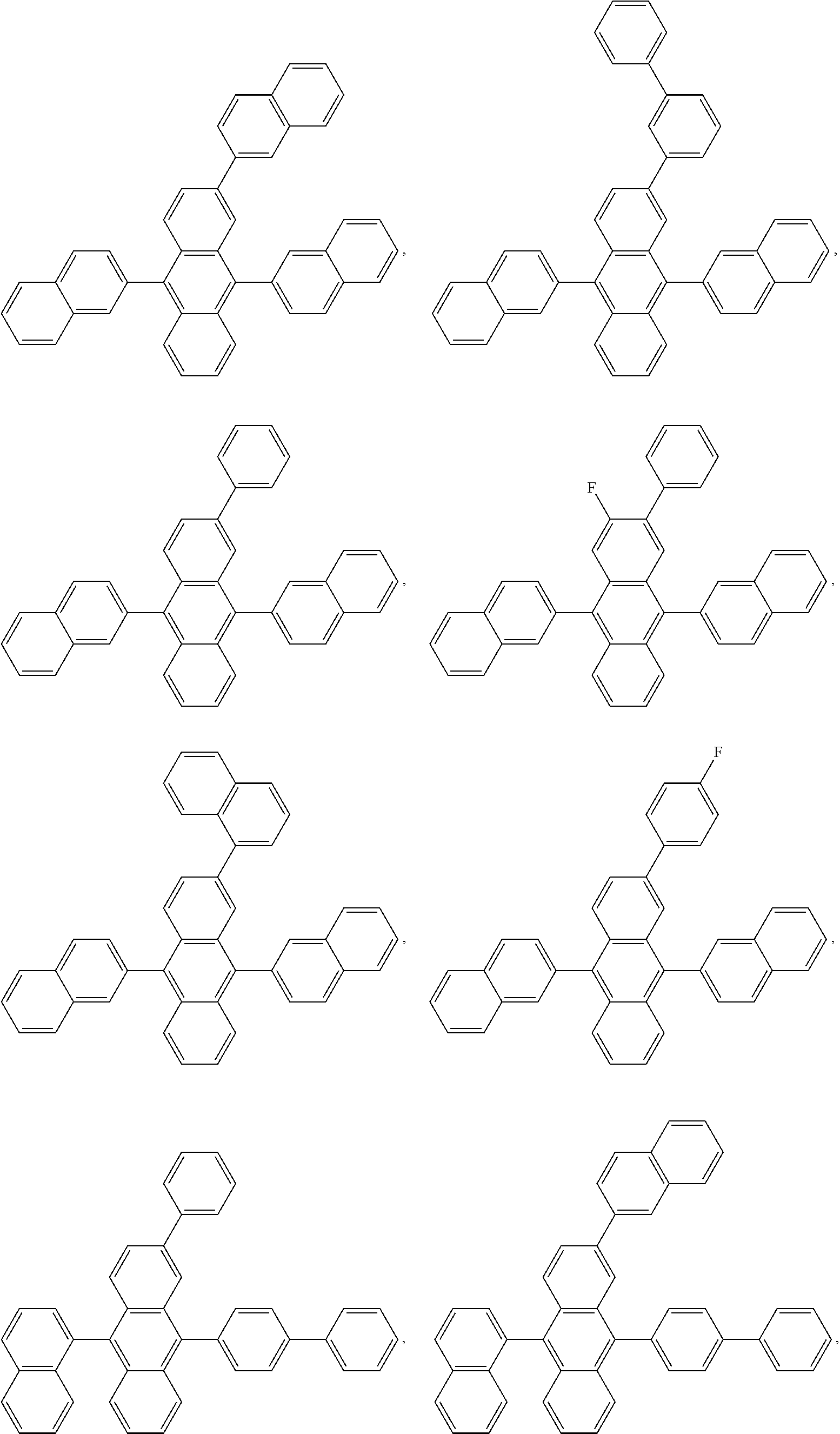


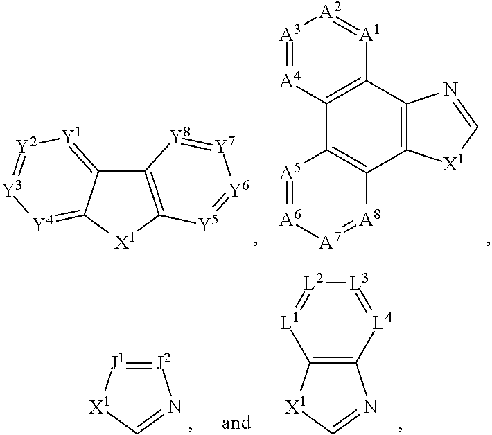


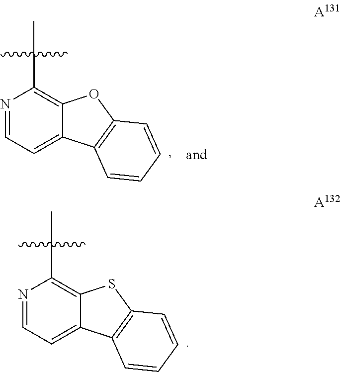


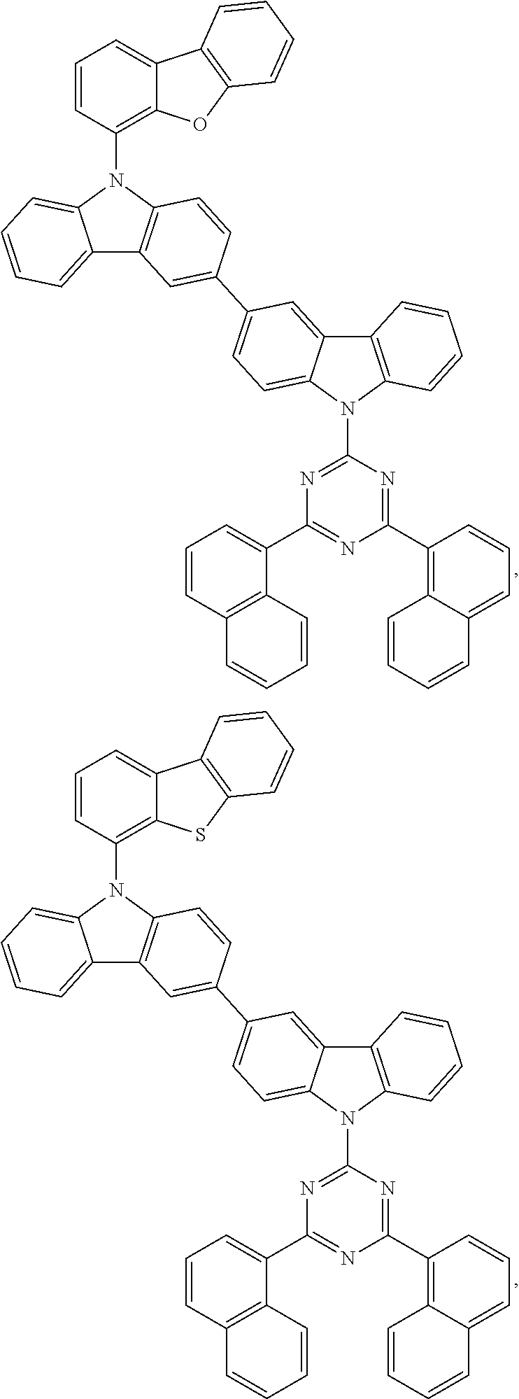


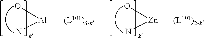


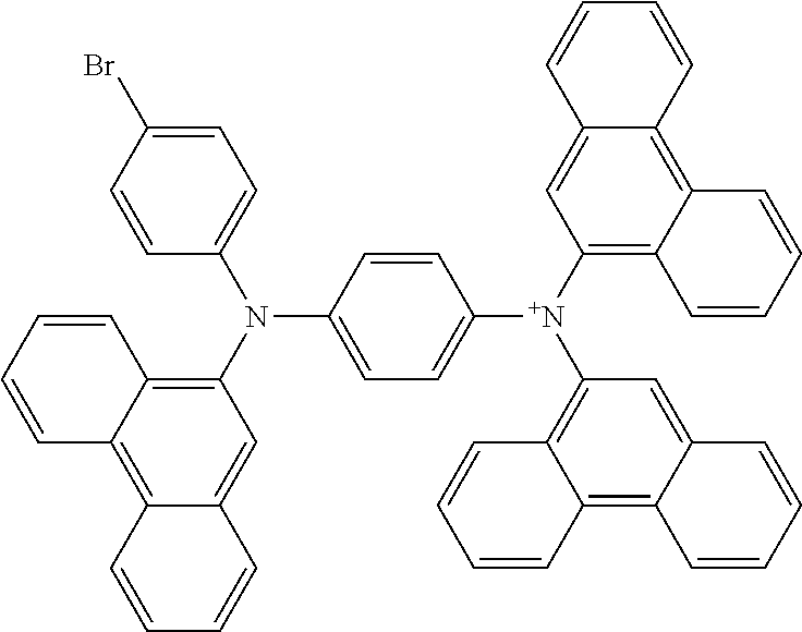


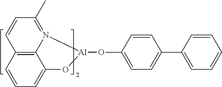
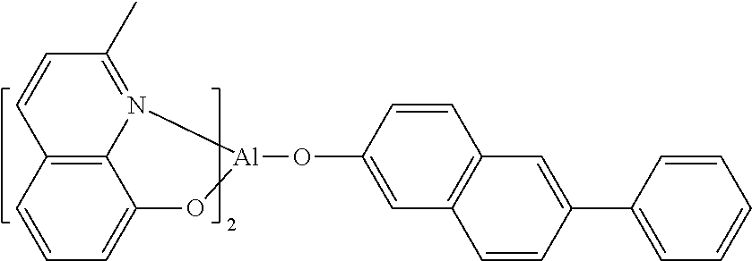


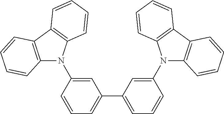


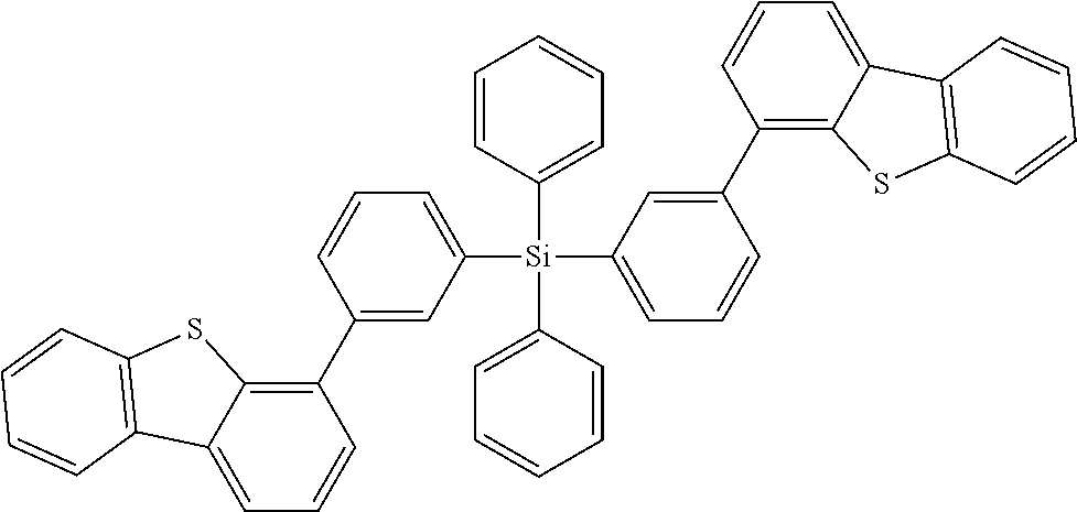


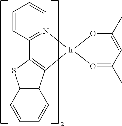


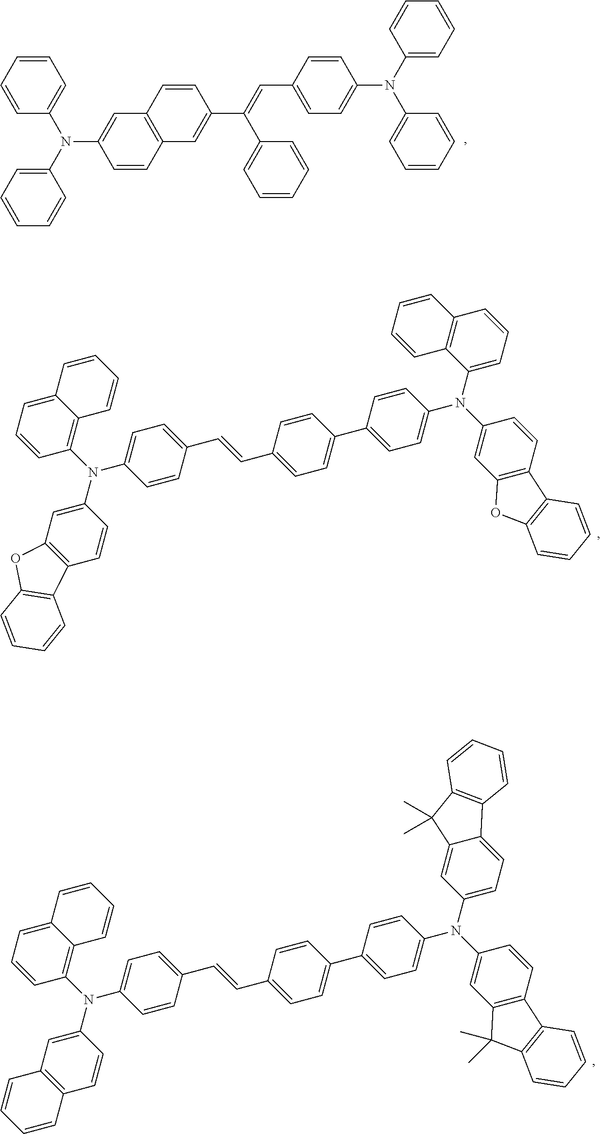
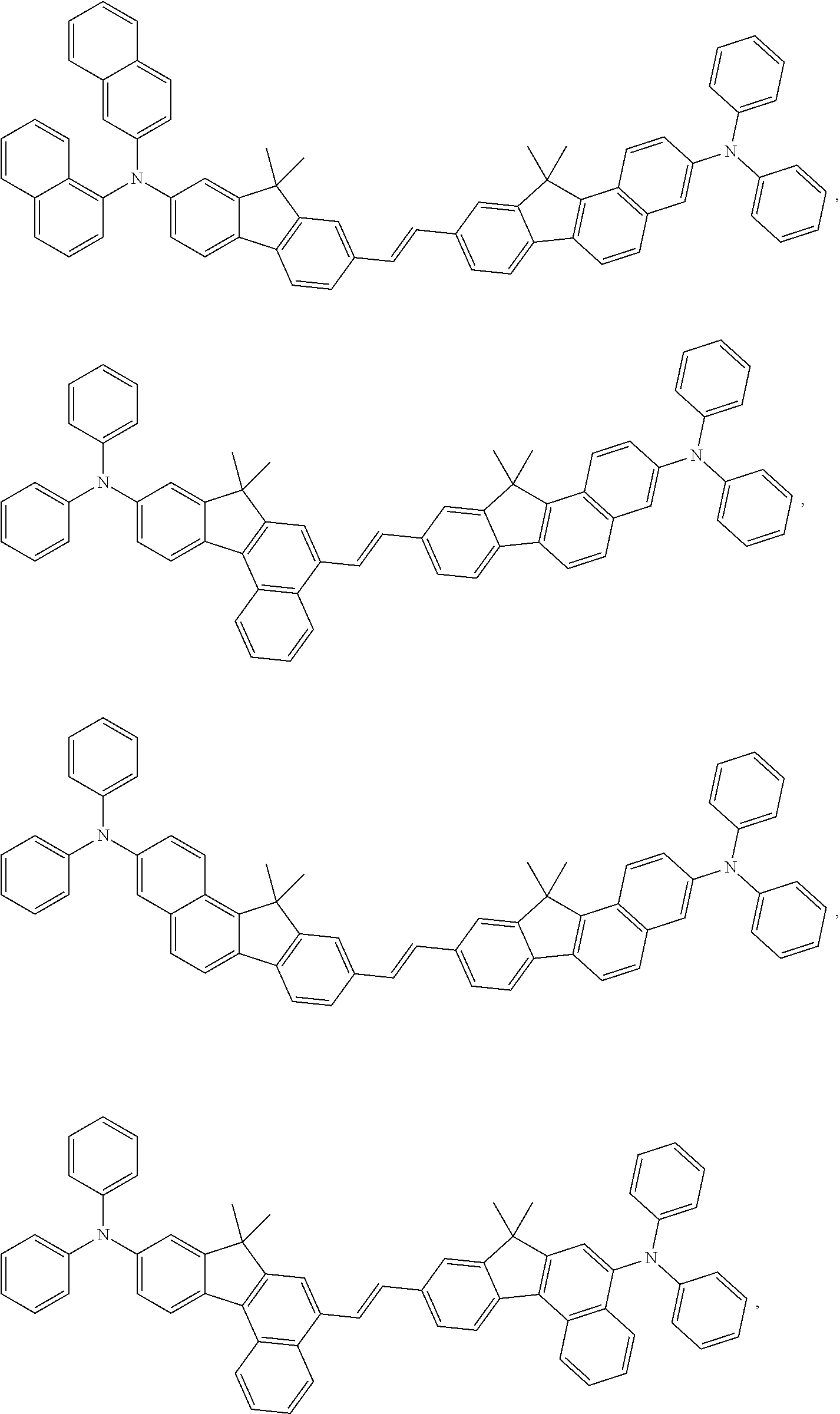


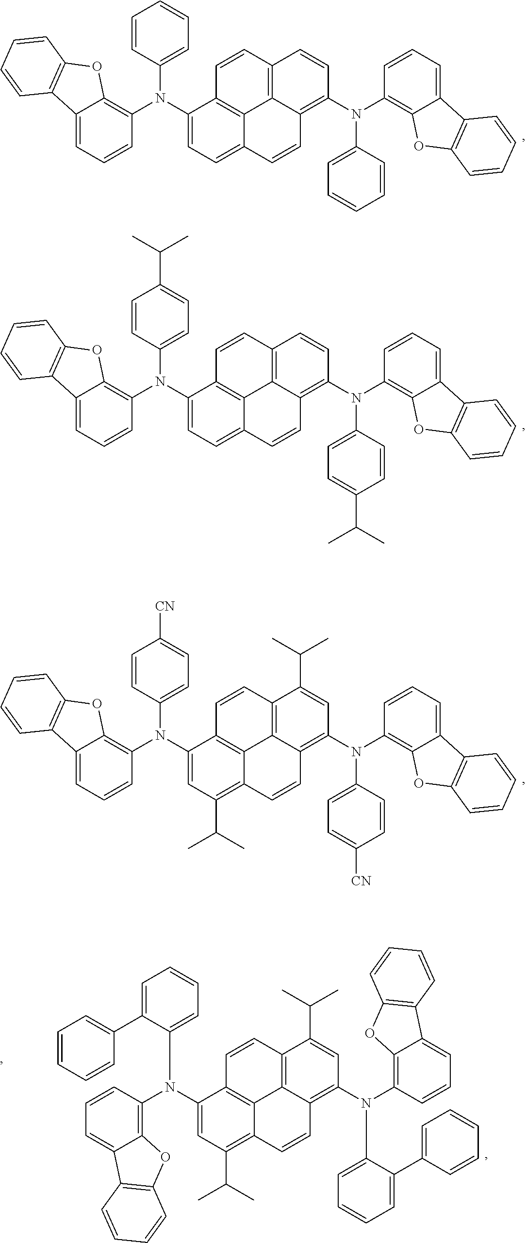


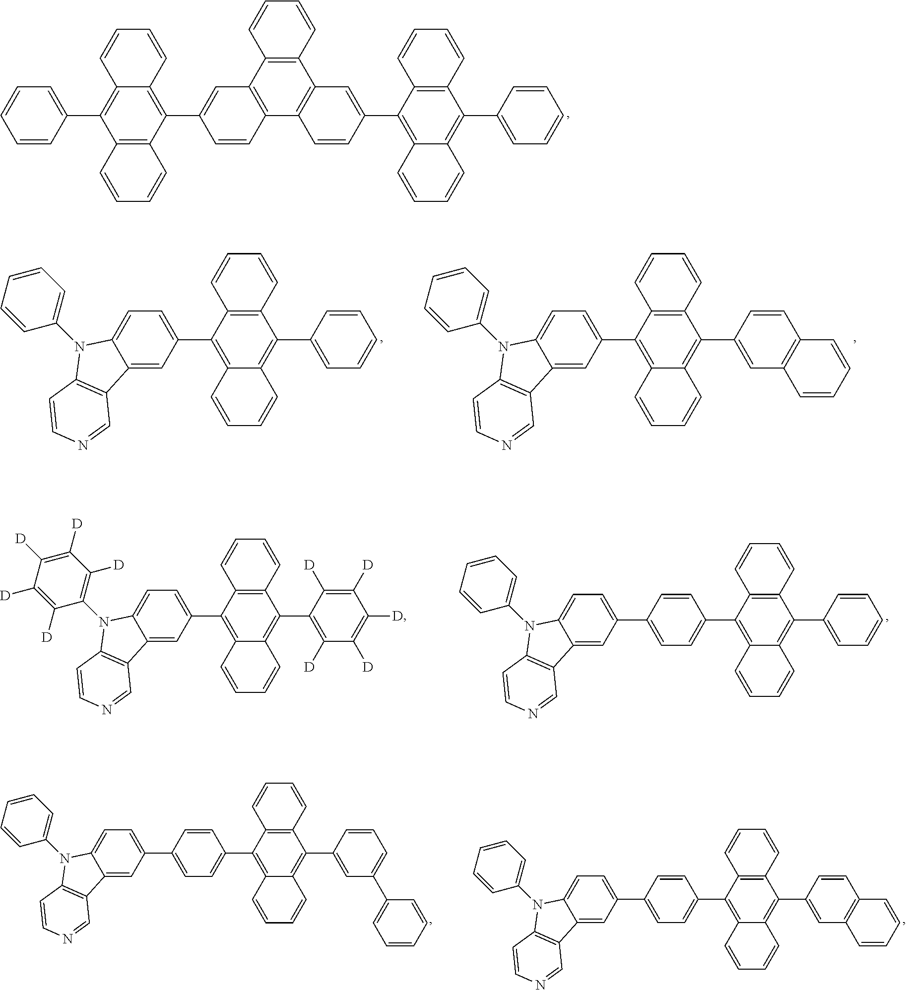


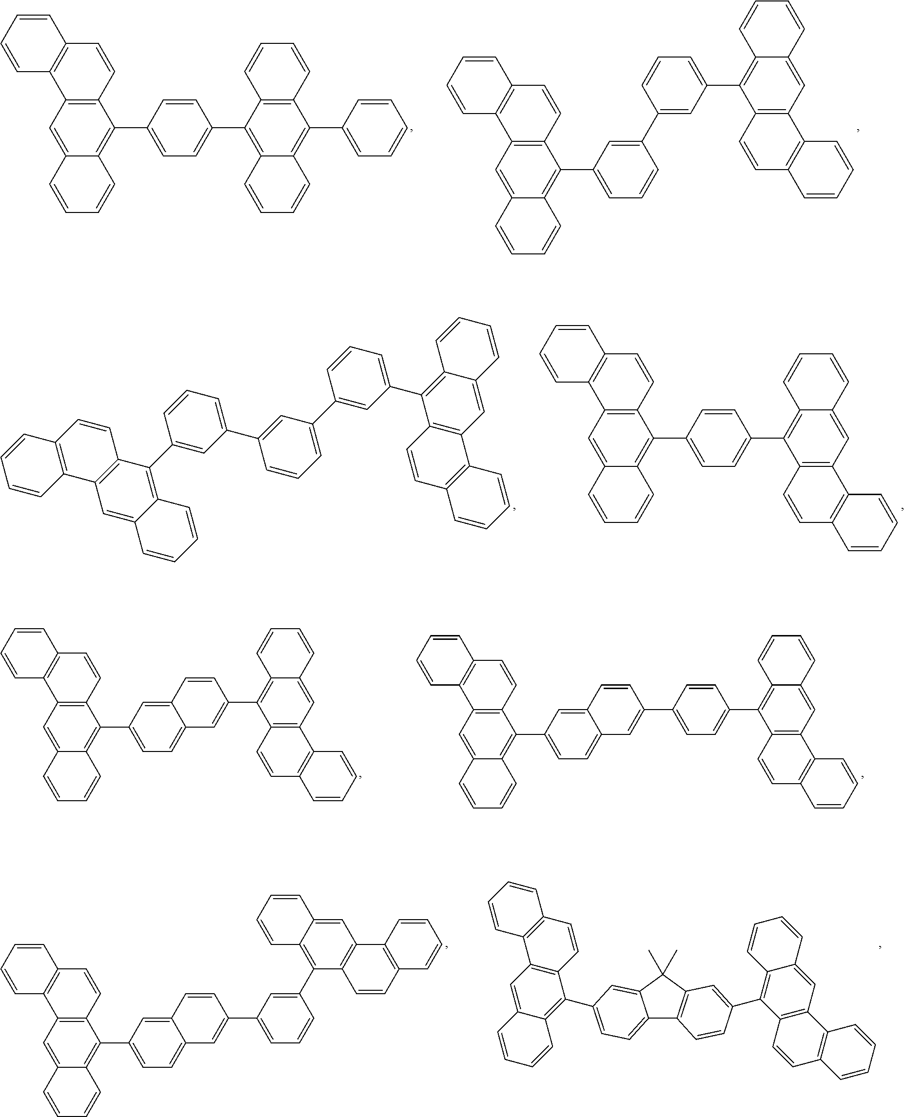


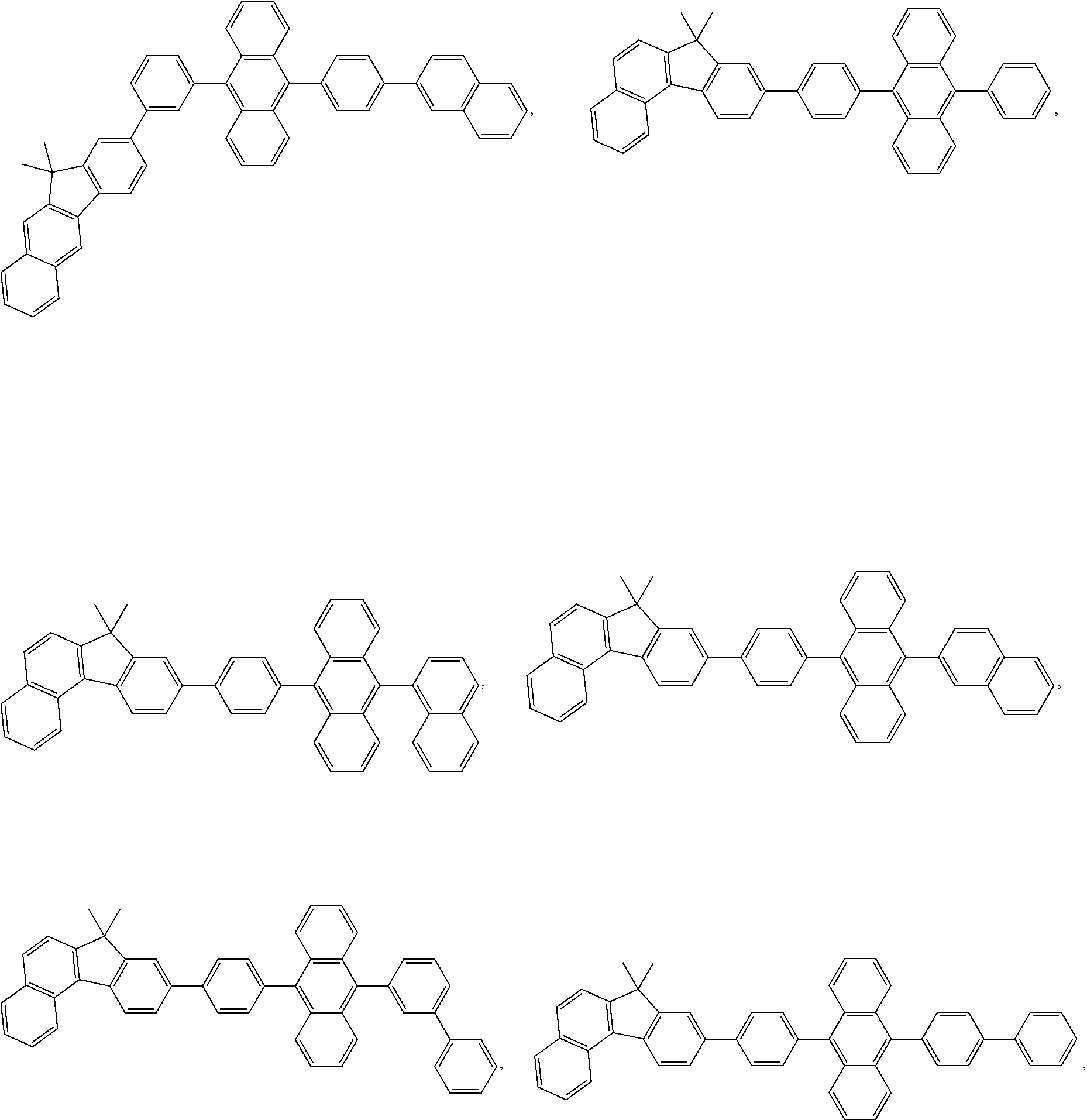


D00000

D00001

D00002

XML
uspto.report is an independent third-party trademark research tool that is not affiliated, endorsed, or sponsored by the United States Patent and Trademark Office (USPTO) or any other governmental organization. The information provided by uspto.report is based on publicly available data at the time of writing and is intended for informational purposes only.
While we strive to provide accurate and up-to-date information, we do not guarantee the accuracy, completeness, reliability, or suitability of the information displayed on this site. The use of this site is at your own risk. Any reliance you place on such information is therefore strictly at your own risk.
All official trademark data, including owner information, should be verified by visiting the official USPTO website at www.uspto.gov. This site is not intended to replace professional legal advice and should not be used as a substitute for consulting with a legal professional who is knowledgeable about trademark law.