Led Array Module
Engelen; Rob Jacques Paul ; et al.
U.S. patent application number 16/472545 was filed with the patent office on 2019-10-17 for led array module. The applicant listed for this patent is Lumileds LLC. Invention is credited to Rob Jacques Paul Engelen, Erno Fancsali, Varun Dev Kakkar, Frans Hubert Konijn, Nicola Bettina Pfeffer, Charles Andre Schrama, Emanuel Nicolaas Hermanus Johannes Stassar.
| Application Number | 20190319019 16/472545 |
| Document ID | / |
| Family ID | 60937699 |
| Filed Date | 2019-10-17 |


| United States Patent Application | 20190319019 |
| Kind Code | A1 |
| Engelen; Rob Jacques Paul ; et al. | October 17, 2019 |
LED ARRAY MODULE
Abstract
The invention describes a light emitting diode array module (30) comprising a plurality of light emitting diode structures (10a, 10b), wherein the light emitting diode structures (10a, 10b) are arranged such that there is an optical cross talk between the light emitting diode structures (10a, 10b) during operation of the light emitting diode array module (30), wherein at least a first light emitting diode structure (10a) of the plurality of light emitting diode structures (10a, 10b) is characterized by a first color, and wherein at least a second light emitting diode structure (10b) of the plurality of light emitting diode structures (10a, 10b) is characterized by a second color different than the first color, wherein the first color, the second color and the optical cross talk between the light emitting diodes are arranged to provide a predefined light distribution in a reference plane (40) perpendicular to an optical axis (50) of the light emitting diode array module (30). The invention further describes a lighting device comprising one or more LED array modules (30).
| Inventors: | Engelen; Rob Jacques Paul; (Eindhoven, NL) ; Konijn; Frans Hubert; (Eindhoven, NL) ; Schrama; Charles Andre; (San Jose, CA) ; Stassar; Emanuel Nicolaas Hermanus Johannes; (Sprang Capelle, NL) ; Fancsali; Erno; (Heusden-Zolder, BE) ; Kakkar; Varun Dev; (Eindhoven, NL) ; Pfeffer; Nicola Bettina; (Eindhoven, NL) | ||||||||||
| Applicant: |
|
||||||||||
|---|---|---|---|---|---|---|---|---|---|---|---|
| Family ID: | 60937699 | ||||||||||
| Appl. No.: | 16/472545 | ||||||||||
| Filed: | December 13, 2017 | ||||||||||
| PCT Filed: | December 13, 2017 | ||||||||||
| PCT NO: | PCT/EP2017/082635 | ||||||||||
| 371 Date: | June 21, 2019 |
Related U.S. Patent Documents
| Application Number | Filing Date | Patent Number | ||
|---|---|---|---|---|
| 62437454 | Dec 21, 2016 | |||
| Current U.S. Class: | 1/1 |
| Current CPC Class: | H01L 33/62 20130101; H01L 33/32 20130101; H01L 33/502 20130101; H01L 33/50 20130101; H01L 25/0753 20130101; H01L 33/06 20130101; H01L 33/505 20130101 |
| International Class: | H01L 25/075 20060101 H01L025/075; H01L 33/50 20060101 H01L033/50 |
Foreign Application Data
| Date | Code | Application Number |
|---|---|---|
| Jan 9, 2017 | EP | 17150666.0 |
Claims
1-11. (canceled)
12. An apparatus, comprising: an array of light emitting diodes (LEDs), the LEDs configured to produce primary light having a primary wavelength, the LEDs including a phosphor configured to absorb at least a portion of primary light that strikes the phosphor and, in response to said absorption, emit secondary light having a wavelength longer than the primary wavelength, the LEDs further configured to emit emitted light that is a combination of the primary light and the secondary light, the emitted light having a correlated color temperature determined by a ratio of primary light to secondary light, the array of LEDs configured such that at least some of the LEDs direct a portion of the produced light to adjacent LEDs as crosstalk light, the array of LEDs configured to control a correlated color temperature of the LEDs by controlling a level of the primary light produced by each LED based at least in part on a level of the crosstalk light received at the LED.
13. The apparatus of claim 12, wherein, for a first LED of the array of LEDs, the level of crosstalk light received at the first LED is determined in part by a number of LEDs in the array that direct crosstalk light onto the first LED.
14. The apparatus of claim 12, wherein, for a first LED of the array of LEDs, the level of crosstalk light received at the first LED is proportional to a number of LEDs in the array that direct crosstalk light onto the first LED.
15. The apparatus of claim 12, wherein: the array has a central area and a border area surrounding the central area; the LEDs in the array are distributed between a central group of LEDs positioned in the central area and a border group of LEDs positioned in the border area; and the array of LEDs is further configured to set a level of primary light produced by the central group of LEDs to a first level and set a level of primary light produced by the border group of LEDs to a second level different from the first level.
16. The apparatus of claim 15, wherein the second level is greater than the first level.
17. The apparatus of claim 15, wherein: each LED in the central group is fully surrounded by adjacent LEDs in the array of LEDs; and each LED in the border group is only partially surrounded by adjacent LEDs in the array of LEDs.
18. The apparatus of claim 15, wherein: the LEDs are positioned in a rectilinear array; each LED in the central group is surrounded by four directly adjacent LEDs and four diagonally adjacent LEDs in the array of LEDs; and each LED in the border group is surrounded by fewer than four directly adjacent LEDs or fewer than four diagonally adjacent LEDs in the array of LEDs.
19. The apparatus of claim 12, wherein: each LED in the array is configured to emit light from a first emission surface oriented generally parallel to the array and from at least one second emission surface oriented substantially orthogonal to the first emission surface; and the LEDs are arranged in the array such that the at least one second emission surface of least some LEDs in the array are positioned to receive light from the at least one second emission surface of at least another LED in the array.
20. The apparatus of claim 19, wherein light emitted from a secondary emission surface of a first LED of the array is configured to produce a phosphor interaction on a second LED of the array.
21. The apparatus of claim 19, wherein light emitted from a secondary emission surface of a first LED of the array is configured to be absorbed by a second LED of the array.
22. A method, comprising: producing, with an array of light emitting diodes (LEDs), primary light having a primary wavelength; absorbing, with a phosphor included with the array, at least a portion of primary light that strikes the phosphor; emitting, with the phosphor, in response to said absorption, secondary light having a wavelength longer than the primary wavelength; emitting, with the LEDs in the array, emitted light that is a combination of the primary light and the secondary light, the emitted light having a correlated color temperature determined by a ratio of primary light to secondary light; directing a portion of the emitted light to adjacent LEDs in the array as crosstalk light; and controlling a correlated color temperature of the LEDs by controlling a level of the primary light produced by each LED based at least in part on a level of the crosstalk light received at the LED.
23. The method of claim 22, wherein, for a first LED of the array of LEDs, the level of crosstalk light received at the first LED is determined in part by a number of LEDs in the array that direct crosstalk light onto the first LED.
24. The method of claim 22, wherein, for a first LED of the array of LEDs, the level of crosstalk light received at the first LED is proportional to a number of LEDs in the array that direct crosstalk light onto the first LED.
25. The method of claim 22, wherein: the array has a central area and a border area surrounding the central area; the LEDs in the array are distributed between a central group of LEDs positioned in the central area and a border group of LEDs positioned in the border area; and further comprising: setting a level of primary light produced by the central group of LEDs to a first level; and setting a level of primary light produced by the border group of LEDs to a second level different from the first level.
26. The method of claim 25, wherein the second level is greater than the first level.
27. The method of claim 25, wherein: each LED in the central group is fully surrounded by adjacent LEDs in the array of LEDs; and each LED in the border group is only partially surrounded by adjacent LEDs in the array of LEDs.
28. The method of claim 25, wherein: the LEDs are positioned in a rectilinear array; each LED in the central group is surrounded by four directly adjacent LEDs and four diagonally adjacent LEDs in the array of LEDs; and each LED in the border group is surrounded by fewer than four directly adjacent LEDs or fewer than four diagonally adjacent LEDs in the array of LEDs.
29. The method of claim 22, wherein: each LED in the array is configured to emit light from a first emission surface oriented generally parallel to the array and from at least one second emission surface oriented substantially orthogonal to the first emission surface; and the LEDs are arranged in the array such that the at least one second emission surface of least some LEDs in the array are positioned to receive light from the at least one second emission surface of at least another LED in the array.
30. An apparatus, comprising: a rectilinear array of light emitting diodes (LEDs) that are configured to produce light and direct a portion of the produced light to adjacent LEDs in the array as crosstalk light, the array having a central area and a border area surrounding the central area, the LEDs in the array being distributed between a central group of LEDs positioned in the central area and a border group of LEDs positioned in the border area, each LED in the central group being surrounded by four directly adjacent LEDs and four diagonally adjacent LEDs in the array of LEDs, each LED in the border group being surrounded by fewer than four directly adjacent LEDs or fewer than four diagonally adjacent LEDs in the array of LEDs, the array of LEDs configured to control a correlated color temperature of the LEDs by setting a level of primary light produced by the central group of LEDs to a first level and setting a level of primary light produced by the border group of LEDs to a second level greater than the first level.
31. The apparatus of claim 30, wherein: each LED in the array is configured to emit light from a first emission surface oriented generally parallel to the array and from at least one second emission surface oriented substantially orthogonal to the first emission surface; and the LEDs are arranged in the array such that the at least one second emission surface of least some LEDs in the array are positioned to receive light from the at least one second emission surface of at least another LED in the array.
Description
FIELD OF THE INVENTION
[0001] The invention relates to a light emitting diode (LED) array module. The invention further relates to a lighting device comprising one or more LED array modules.
BACKGROUND OF THE INVENTION
[0002] The human eye is very sensitive with respect to variations in a light distribution or illumination pattern provided by a light source. Homogeneity of the correlated color temperature of the light distribution provided by a lighting module is therefore an important quality criterion. Especially lighting modules comprising a multitude of light emitters like light emitting diode (LED) structures require a careful selection of these LED structures in order to enable a homogeneous distribution of the color and especially of the correlated color temperature in a defined sector of the space illuminated by the lighting modules.
[0003] US 2012/0106145 A1 discloses an operating light which includes at least one first radiation source, which is suitable for producing light with locally different, especially radially outwardly decreasing color temperature distribution in a plane extending at right angles to the work area.
SUMMARY OF THE INVENTION
[0004] It is an object of the present invention to provide a light emitting diode (LED) array module with improved distribution of the color especially the correlated color temperature.
[0005] The invention is described in the independent claims. The dependent claims comprise preferred embodiments.
[0006] According to a first aspect a light emitting diode (LED) array module is provided. The LED array module comprises a plurality of light emitting diode structures. The light emitting diode structures are arranged such that there is an optical cross talk between the light emitting diode structures during operation of the light emitting diode array module. At least a first light emitting diode structure of the plurality of light emitting diode structures is characterized by a first color or flux. At least a second light emitting diode structure of the plurality of light emitting diode structures is characterized by a second color different than the first color. The at least second light emitting diode structure of the plurality of light emitting diode structures may alternatively or in addition be characterized by a second flux different than the first flux. The first color or the first flux, the second color or the second flux and the optical cross talk between the light emitting diodes are arranged to provide a predefined light distribution and preferably a predefined color distribution in a reference plane perpendicular to an optical axis of the light emitting diode array module. The reference plane is arranged at a defined distance to the light emitting diode array module.
[0007] The color of one of the LED structures may be preferably be characterized by the color temperature, correlated color temperature and the like. Especially the correlated color temperature may be preferred to characterize a LED module emitting white light.
[0008] Classic high-power LED structures are simple surface emitting light sources. However, these structures are getting smaller as time progresses, which is mostly cost-driven. One of the features that are allowing for further cost-down is 5-sided emission. Where a conventional LED structure would only emit from the top, a 5-sided emitter would also emit from the sides.
[0009] Such novel emitters have advantages in cost, but also in design flexibility. One could for example envisage a close-packed array of these emitters to achieve a very high-density high-flux emitter array.
[0010] Because of the 5-sided emission, light exiting the side of an emitter has a reasonable chance of entering a neighboring LED. The light entering its neighbor will interact with the neighboring LED which can result in a change of color and/or a change of flux. Such a change may be caused by phosphor interaction in the second LED structure and/or absorption of light in the second LED structure.
[0011] An LED structure at the edge of an array will therefore be affected less than an LED structure in the middle of the array.
[0012] This may result in: [0013] An array with a total flux and average color point that is different from the LEDs when used in isolation. [0014] Over the array, the flux and color will vary. Color variation over the array is unwanted as it may result in non-uniform spot lighting.
[0015] The LED array module described above avoids or at least reduces the problem of color (flux) variation by taking into account the influence of neighboring LED structures in the LED array module. The LED structures are characterized by different (e.g. first, second, third, fourth etc.) colors or correlated color temperatures and optionally first, second, third, fourth fluxes which are combined in a way that the interaction between the LED structures is taking into account in order to provide the predefined color point and optionally flux distribution. The predefined correlated color temperature distribution may, for example, be a homogeneous or uniform correlated color temperature distribution or it may be a non-uniform color point distribution (e.g. a cool white correlated color temperature in a center and a warm white correlated color temperature at a border of the light distribution provided by means of the LED array module).
[0016] The correlated colors or color temperature of the LED structures and/or the fluxes may be chosen based on the binning of the different LED structures. That means that LED structures with, for example, different correlated color temperatures and/or fluxes are combined, wherein the difference of the correlated color temperatures and/or fluxes is caused by variations in the production process of the LED structures. Alternatively, LED structures with different semiconductor layers (e.g. composition of active layer) and/or different light conversion structure may be combined in order to enable the predefined distribution of the color and especially the correlated color temperature and/or fluxes of the LED array module.
[0017] The first, second, third etc. color or correlated color temperature and/or fluxes of the LED structures refers to the color, or correlated color temperature of an isolated LED structure without any interaction with neighboring LED structures.
[0018] At least the first light emitting diode structure of the plurality of light emitting diode structures may be further characterized by a first flux. At least a third light emitting diode structure of the plurality of light emitting diode structures may be characterized by a third flux. The first flux, the third flux and the optical cross talk between the light emitting diodes may be arranged to provide the predefined light distribution in the reference plane. The third LED structure may be the same as the second LED structure or a different LED structure. The third LED structure may be further characterized by a third color or correlated color temperature different than the first and/or second color or correlated color temperature.
[0019] The predefined light distribution may comprise a predefined color point temperature distribution. The first correlated color temperature and the second correlated color temperature may be arranged to at least partly compensate the optical cross talk between the light emitting diode structures such that a homogeneity of the predefined color point temperature distribution is increased.
[0020] The optical cross talk between the LED structures may cause an unintended shift of the correlated color temperature of neighboring LED structures. This unintended shift may be compensated by providing 2, 3, 4 or more LED structures with different correlated color temperatures.
[0021] The light emitting diode structures may be arranged to emit primary light and secondary light. The primary light is characterized by a first center wavelength in a first wavelength range. The secondary light is characterized by a second center wavelength in a second wavelength range. The second wavelength range is in a longer wavelength range than the first wavelength range. The at least first correlated color temperature and the at least second correlated color temperature are determined based on a probability that a light emitting diode structure receives primary light from one or more light emitting diode structures encompassing the light emitting diode structure.
[0022] The probability may be determined based on a number of the light emitting diode structures encompassing the light emitting diode structure.
[0023] The probability may alternatively or in addition be determined based on a distance between the light emitting diode structures encompassing the light emitting diode structure and the light emitting diode structure.
[0024] The probability may alternatively or in addition be determined based on a relative position of the light emitting diode structures encompassing the light emitting diode structure with respect to the light emitting diode structure.
[0025] The probability of receiving light and especially primary or secondary light is in general determined by the illumination pattern of each single LED structure and the geometric arrangement of the LED structures within the LED array module. Symmetry of the LED structures within the LED array module, varying distances lengths of common border between neighboring LED structures influence the probability that, for example, primary light is received by a light conversion structure of a neighboring (encompassing) LED structure. Furthermore, the arrangement of the LED structures may influence emission of secondary light which may be emitted after conversion of primary light received from a neighboring LED structure. In addition there may be optical structures especially at the border of a LED array module which may be arranged to reflect, for example, primary light emitted by LED structures at the border back to the emitting LED structure or a neighboring LED structure of the emitting LED structure. The optical structure or structures may especially be arranged to approximately mimic a neighboring LED. The optical structure may have in this case the effect that, for example, primary light emitted by a LED structure is reflected such that it appears for the emitting LED structure and neighboring LED structures that there is one or more LED structure at the position of the optical structure. The optical structure or structures provide a kind of image of the LED structures at the border of the LED array module.
[0026] A correlated color temperature of the light emitting diode structure encompassed by the light emitting structures may be higher the higher the probability of receiving primary light from the encompassing light emitting diode structures is.
[0027] The probability of receiving, for example, primary light from LED structures by means of a light conversion structure (e.g. phosphor layer) and the probability of conversion of this primary light to secondary light determine the amount of additional secondary light which is emitted by the light conversion structure of the respective LED structure. It may therefore be necessary to shift the correlated color temperature of an LED structure with a high probability of emitting additional secondary light based on the primary light received from encompassing LED structures to higher correlated color temperatures. The higher correlated color temperature may be chosen such that the ratio between primary light and secondary light emitted by the LED structure encompassed by the other LED structures is essentially the same as a ratio of the primary light and secondary light emitted by the encompassing LED structures (taking into account the cross talk between all neighboring LED structures).
[0028] The predefined correlated color temperature distribution may be flat within a defined distance from the optical axis. The first, second, third, fourth or more different correlated color temperatures of the LED structures may be used to extend the sector of uniform correlated color temperature of a lighting pattern provided by a LED array structure. The predefined correlated color temperature distribution may in this case be flat in the reference plane around the optical axis. The different (lower) correlated color temperature of LED structures at the border of the array may extend the distance from the optical axis in the reference plane in which the predefined correlated color temperature distribution is flat.
[0029] The light emitting diode array module may comprise a multitude of light emitting diode structures arranged in a regular pattern. The regular pattern of light emitting diode structures comprises a central area and a border area. A correlated color temperature of light emitting diode structures comprised by the border area is arranged to at least partly compensate the optical cross talk in accordance with a correlated color temperature distribution provided by light emitting diode structures comprised by the central area.
[0030] The light emitting structures of the LED array module may be characterized by, for example sub arrays with different emission characteristics. The correlated color temperature of the LED array module in the central area may, for example, be determined by the intensity provided by the different sub arrays of LED structures. LED structures comprised by the border area of the LED array module are characterized by different correlated color temperatures of the respective sub array in comparison to the central area in order to compensate changes of the correlated color temperature caused by varying optical cross talk caused by the geometric arrangement of encompassing LED structures as described above.
[0031] According to a further aspect a lighting device is provided. The lighting device comprises one, two, three or more light emitting diode array modules as described above. The lighting device further comprises at least one optical device being arranged to distribute light emitted by the at least one light emitting diode array module. The optical device may be a single lens or a complex arrangement of lenses, apertures and the like.
[0032] According to a further aspect a method of emitting light with a homogeneous color point distribution by means of a light emitting diode array module comprising a plurality of light emitting diode structures is provided. The method comprises the steps of:
[0033] emitting light of a first correlated color temperature by means of at least a first light emitting diode structure of the plurality of light emitting diode structures such that there is an optical cross talk with at least a second light emitting diode structure,
[0034] emitting light of a second correlated color temperature different than the first correlated color temperature by means of at least the second light emitting diode structure of the plurality of light emitting diode structures such that there is an optical cross talk with at least the first light emitting diode structure, wherein the first correlated color temperature and the second correlated color temperature are arranged to at least partly compensate the optical cross talk between the light emitting diode structures such that a homogeneity of a predefined correlated color temperature distribution in a reference plane perpendicular to an optical axis of the light emitting diode array module is increased.
[0035] It shall be understood that the light emitting diode array module of any one of claims 1-10 and the method of claim 11 have similar and/or identical embodiments, in particular, as defined in the dependent claims.
[0036] It shall be understood that a preferred embodiment of the invention can also be any combination of the dependent claims with the respective independent claim.
[0037] Further advantageous embodiments are defined below.
BRIEF DESCRIPTION OF THE DRAWINGS
[0038] These and other aspects of the invention will be apparent from and elucidated with reference to the embodiments described hereinafter.
[0039] The invention will now be described, by way of example, based on embodiments with reference to the accompanying drawings.
[0040] In the drawings:
[0041] FIG. 1 shows a principal sketch of a light emitting diode structure
[0042] FIG. 2 shows a principal sketch of a light emitting diode array
[0043] FIG. 3 shows a principal sketch of a first embodiment of a LED array module
[0044] FIG. 4 shows a principal sketch of a second embodiment of the LED array module
[0045] FIG. 5 shows a principal sketch of a third embodiment of the LED array module
[0046] FIG. 6 shows a principal sketch of a cross-section of a fourth embodiment of the LED array module
[0047] FIG. 7 shows a first embodiment of a predefined correlated color temperature distribution
[0048] In the Figures, like numbers refer to like objects throughout. Objects in the Figures are not necessarily drawn to scale.
DETAILED DESCRIPTION OF EMBODIMENTS
[0049] Various embodiments of the invention will now be described by means of the Figures.
[0050] FIG. 1 shows a principal sketch of a cross-section of a light emitting diode (LED) structure 10. The LED structure 10 comprises a n-layer 3 which can be electrically contacted by means of n-contact 5. The n-layer 3 is followed by active layer 4. The active layer 4 may comprise a Quantum Well structure which is arranged to emit light with a wavelength which is determined by the composition of the active layer (e.g., AIInGaN). The active layer 4 is embedded or sandwiched between the n-layer 3 and a p-layer 7. The p-layer 7 can be electrically contacted by means of p-contact 9. The arrangement of n-layer 3, active layer 4, p-layer 9, n-contact 5 and p-contact 9 build a LED die. There may be further support layers which are not shown. A light conversion structure 1 is attached to a top surface of the n-layer 3 which is opposite to surface of the n-layer 3 attached to the active layer 4. The top surface of the n-layer 3 is the light emitting surface of the LED die. The light conversion structure 1 may comprise a phosphor like a Cerium doped phosphor garnet (YAG:Ce). The light conversion structure 1 is arranged to convert primary light 11 (e.g. blue light) emitted by the active layer 4 to secondary light 12 (e.g. yellow light) characterized by a longer wavelength than the primary light 11. A predefined part of the primary light 11 passes light conversion structure 1 without being converted such that the LED structure emits a mixture of primary light 11 and secondary light 12 (white light). The LED structure 10 is arranged to emit at least a major part of the light via a top surface and the side surfaces of the light conversion structure 1, wherein the top surface is opposite to the surface of the light conversion structure 1 which is attached to the n-layer 3. A LED structure 10 with a rectangular or quadratic cross-section perpendicular to the cross-section shown in FIG. 1 comprises therefore five light emission surfaces.
[0051] Alternatively, a kind of lid comprising the phosphor material may be arranged around the LED die of the LED structure 10 such that a mixture of primary and secondary light is emitted by means of different sides of the LED structure 10. Furthermore, the LED structure 10 may be embedded in a transparent light distribution structure which is arranged to emit light and essentially all directions of the semi-sphere in the direct direction of light emission of the LED structure 10.
[0052] FIG. 2 shows a principal sketch of a cross-section of a light emitting diode array 30. The light emitting diode array 30 comprises a number of LED structures 10 (three are shown in the cross-section) attached to a submount 20. The submount 20 comprises a submount chip 21 on which the LED structures 10 are mounted and electrical contact pads 23 by means of which the n-contacts and p-contacts (not shown) of the LED structures 10 can be electrically connected. The LED structures 10 emit primary (blue) light 11 and secondary (yellow) light 12. A part of the primary light 11 emitted by the left and the right LED structure 10 may hit the light conversion structure 1 of the LED structure 10 in the middle. The LED structure 10 in the middle therefore receives more primary light 11 from neighboring (or encompassing) LED structures 10 than the LED structures 10 at the left and at the right. The relative fraction of secondary light emitted from the light conversion structure 1 of the LED structure 10 in the middle is therefore increased. The correlated color temperature of the LED structure 10 in the middle seems therefore to be lower than the correlated color temperature of the LED structures on the left and the right side provided that all LED structures 10 are arranged to emit in a single arrangement, for example, white light of the same correlated color temperature. The same applies to the total flux emitted by the LED structures 10 because the LED 10 structure in the middle additionally receives more secondary light than the LED structures 10 on the left and the right side.
[0053] FIG. 3 shows a principal sketch of a top view of a first embodiment of a LED array module 30. The LED array module 30 comprises three LED structures 10a, 10b which are arranged along an axis (linear array) in a similar way as described with respect to FIG. 2. A LED structure 10a is arranged between two LED structures 10b. The LED structure 10a in the middle emits white light with a higher first correlated color temperature in order to compensate a color shift caused by primary light emitted by the two adjacent LED structures 10b emitting white light with a lower second correlated color temperature in comparison to the first correlated color temperature. The second correlated color temperature is chosen such that the amount of additional converted secondary light 12 (see FIG. 2) caused by primary light received by the light conversion structure 1 of the LED structure 10a in the middle is essentially compensated. The correlated color temperature distribution of the light emitting module 30 is therefore more homogeneous or uniform along the axis of the linear array. It is clear that the selection of the first and the second correlated color temperature is determined by the geometric boundary conditions such that a perfect compensation is not possible. The same principal may be used in order to compensate variations of the flux caused by the optical cross talk between neighboring LED structures 10. The flux of the LED structures 10b at the left and the right may, for example, be higher than the optical flux of LED structure 10a in the middle in order to improve homogeneity of the flux of LED array module 30.
[0054] FIG. 4 shows a principal sketch of a top view of a second embodiment of the LED array module 30. The LED array module 30 comprises a symmetric arrangement of LED structures 10a, 10b, 10c, 10d. The LED array module 30 comprises two symmetry axes both crossing a center point of the LED array module 30. Symmetry with respect to the first symmetry axis is in this case different than the symmetry with respect to the second symmetry axis. The LED structures 10a, 10b, 10c, 10d are arranged such that four LED structures 10a with a first correlated color temperature are arranged in the middle of the LED array module 30. The four LED structures 10a are encompassed by 10 LED structures 10b, 10c, 10d. The correlated color temperatures of the LED structures 10b, 10c, 10d is selected based on the relative position to neighboring LED structures 10a, 10b, 10c, 10d, the number of neighboring LED structures 10a, 10b, 10c, 10d and the distance(s) (the distances may, for example, be different in different directions) between the neighboring LED structures 10a, 10b, 10c, 10d.
[0055] The geometry of the arrangement of the LED structures 10a, 10b, 10c, 10d in the LED array 30 determines a probability of receiving primary light from neighboring LED structures 10a, 10b, 10c, 10d. The nearer the distance, the more neighboring LED structures 10a, 10b, 10c, 10d encompass the respective LED structure 10a, 10b, 10c, 10d the higher is the probability to receive primary light from neighboring LED structures 10a, 10b, 10c, 10d. The correlated color temperature of the four LED structures 10a in the middle is therefore the highest. It is intended to provide an essentially uniform correlated color temperature distribution across the LED array module 30 because each of the four LED structures 10a is encompassed by seven other LED structures 10a, 10b, 10c, 10d. The second correlated color temperature of LED structures 10b is lower than the correlated color temperature of the LED structures 10a in the center but higher than the correlated color temperatures of LED structures 10c, 10b because four LED structures 10a, 10c, 10d encompass LED structures 10b such that three sides of LED structure have overlap with sides of the encompassing LED structures 10a, 10c, 10d. The LED structures 10d have a lower correlated color temperature than LED structures 10b but at a higher correlated color temperature than LED structure 10c being characterized by the lowest correlated color temperature of the LED array module 30.
[0056] FIG. 5 shows a principal sketch of a top view of a third embodiment of the LED array module 30. LED array module 30 comprises in this case two sub arrays of LED structures, which are arranged in a checkerboard pattern. The LED structures 17 of the first sub array (bright squares) are arranged to emit light of a first characteristic. The LED structures of the second sub array (dark squares) are arranged to emit light of a second characteristic. Each sub array 17, 18 can be controlled independently from the other sub array. The LED structures 17 of the first sub array may, for example, be arranged to emit light with a first color (e.g. blue). The LED structures 18 of the second sub array may, for example, be arranged to emit light with a second color (e.g yellow). The color of the light emitted by the LED array module 30 can therefore be controlled by means of the relative intensities provided by the two sub arrays. The general problem as discussed with respect to FIGS. 2, 3 and 4 remains the same. The LED array module 30 comprises a central area 16 wherein the LED structures 17, 18 of the central area 16 are each encompassed by the same number and kind of LED structures 17, 18. The LED array module 30 further comprises a border area 15 in which the number of encompassing LED structures 17, 18 depends on the position within the border area 15. The color of the LED structures 17, 18 of the border area 15 are therefore different than the color of the LED structures 17, 18 of the corresponding central area 16 in order to compensate the different optical crosstalk between the LED structures 17, 18. The color of the LED structures 17, 18 of the border area 15 essentially depends on the number of LED structures 17, 18 encompassing the respective LED structure 17, 18. The area of the LED array module 13 appearing to emit light of the same color and correlated color temperature is thus increased. The border area 15 and the central area 16 are separated by a small gap in FIG. 5 in order to simplify identification of LED structures 17, 18 of the central area 16 and the border area 15. There is no such a gap in the real LED array module 30.
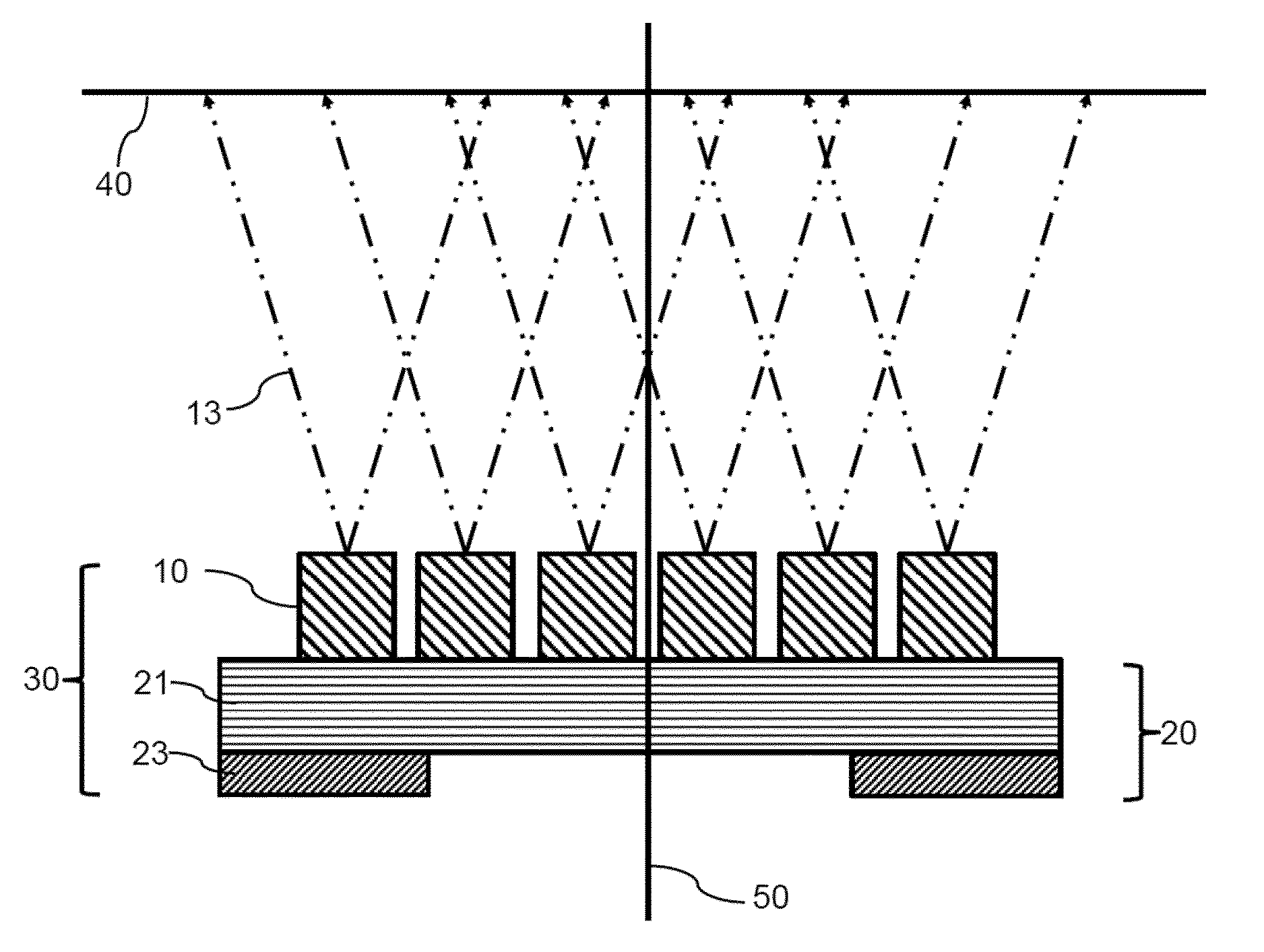
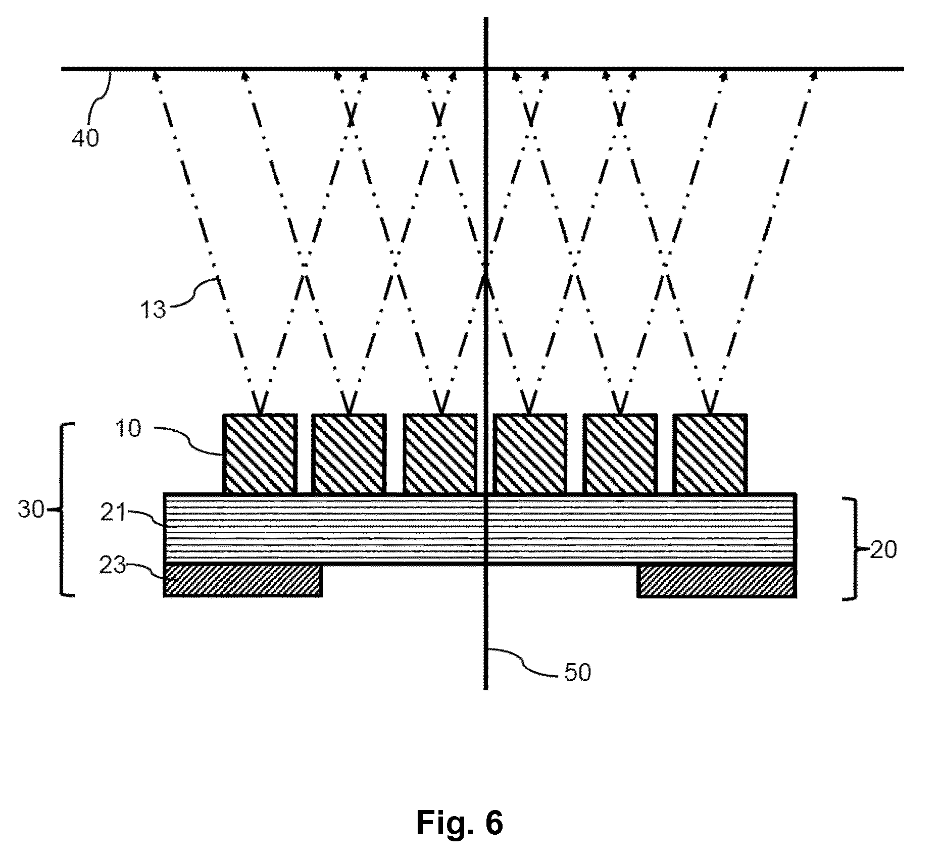
[0057] FIG. 6 shows a principal sketch of a cross-section of a fourth embodiment of the LED array module 30. The LED array module comprises an array of 5x6 LED structures 10. The cross section shows six LED structures 10 in the third of the five lines of LED structures 10 which are arranged in a regular quadratic pattern. The LED structures 10 are attached to a submount 20 comprising a submount chip 21 and electrical contact pads 23 as discussed with respect to FIG. 2. The LED array module 30 comprises an optical axis 50 which is arranged in the middle of the 5.times.6 LED structures 10. Each of the LED structures 10 emits mixed light 13 comprising primary light 11 and secondary light 12 as discussed with respect to FIG. 2. The mixed light 13 overlaps in reference plane 40 which may, for example, be arranged in a distance preferably between 5 mm and 10 mm in order to detect the impact of the LED structures 10 comprised by the LED module 30. The correlated color temperature of the LED structures 10 of the central area of the LED array module 30 is higher in comparison to the correlated color temperature of the LED structures 10 of the border area of the LED array module 30. The LED structures 10 at the four corners of the LED array module 30 are characterized by the lowest correlated color temperature because these LED structures 10 are encompassed by the lowest number of encompassing LED structures 10.
[0058] FIG. 7 shows the predefined correlated color temperature distribution 65 of the LED array module 30 shown in FIG. 6 along an axis of reference plane 40. The axis crosses the optical axis 50 and is arranged along the line defined by the LED structures 10 shown in FIG. 6. The abscissa 61 shows the distance to the optical axis 50 in the reference plane 40 and the ordinate 62 shows the correlated color temperature along the axis in the reference plane 40. The predefined correlated color temperature distribution 65 is essentially constant or flat within a predefined range around the optical axis 50 in the reference plane 40. The predefined range within the reference plane 40 is determined by the illumination pattern provided by each LED structure 10, the geometric orientation of the LED structures 10 within the LED array module 30 and the compensation of the optical cross talk by means of the different correlated color temperature of LED structures 10 in the border area of the LED array module 30.
[0059] Although the disclosure mainly speaks of correlated color temperature to describe the color of LED structures 10, the invention is not limited to colors of a black body radiator. A person skilled in the art will understand that the invention holds for color compensation in the full color space. Typically, the colors mentioned in the disclosure will be along the phosphor load line(s), i.e. the colors one can create by changing the concentration of phosphor in light conversion structure 1 of the corresponding LED structure 10.
[0060] While the invention has been illustrated and described in detail in the drawings and the foregoing description, such illustration and description are to be considered illustrative or exemplary and not restrictive.
[0061] From reading the present disclosure, other modifications will be apparent to persons skilled in the art. Such modifications may involve other features which are already known in the art and which may be used instead of or in addition to features already described herein.
[0062] Variations to the disclosed embodiments can be understood and effected by those skilled in the art, from a study of the drawings, the disclosure and the appended claims. In the claims, the word "comprising" does not exclude other elements or steps, and the indefinite article "a" or "an" does not exclude a plurality of elements or steps. The mere fact that certain measures are recited in mutually different dependent claims does not indicate that a combination of these measures cannot be used to advantage.
[0063] Any reference signs in the claims should not be construed as limiting the scope thereof.
LIST OF REFERENCE NUMERALS
[0064] 1 light conversion structure [0065] 3 n-layer [0066] 4 active layer [0067] 5 n-contact [0068] 7 p-layer [0069] 9 p-contact [0070] 10 light emitting diode (LED) structure [0071] 10a LED structure with first correlated color temperature [0072] 10b LED structure with second correlated color temperature [0073] 10c LED structure with third correlated color temperature [0074] 10d LED structure with fourth correlated color temperature [0075] 11 primary light [0076] 12 secondary light [0077] 13 mixed light [0078] 15 light emitting diode structure of border area [0079] 16 light emitting diode structure of central area [0080] 17 LED structure of first sub array [0081] 18 LED structure of second sub array [0082] 20 submount [0083] 21 submount chip [0084] 23 electrical contact pads [0085] 30 light emitting diode (LED) array module [0086] 40 reference plane [0087] 50 optical axis [0088] 61 distance to optical axis in reference plane [0089] 62 correlated color temperature in reference plane [0090] 65 correlated color temperature distribution in reference plane
* * * * *
D00000
D00001
D00002
D00003
D00004
D00005
XML
uspto.report is an independent third-party trademark research tool that is not affiliated, endorsed, or sponsored by the United States Patent and Trademark Office (USPTO) or any other governmental organization. The information provided by uspto.report is based on publicly available data at the time of writing and is intended for informational purposes only.
While we strive to provide accurate and up-to-date information, we do not guarantee the accuracy, completeness, reliability, or suitability of the information displayed on this site. The use of this site is at your own risk. Any reliance you place on such information is therefore strictly at your own risk.
All official trademark data, including owner information, should be verified by visiting the official USPTO website at www.uspto.gov. This site is not intended to replace professional legal advice and should not be used as a substitute for consulting with a legal professional who is knowledgeable about trademark law.