Method and Apparatus for the Monolithic Encapsulation of a Micro-Scale Inertial Navigation Sensor Suite
KIRBY; Deborah J. ; et al.
U.S. patent application number 16/376970 was filed with the patent office on 2019-10-17 for method and apparatus for the monolithic encapsulation of a micro-scale inertial navigation sensor suite. This patent application is currently assigned to HRL Laboratories, LLC. The applicant listed for this patent is HRL Laboratories, LLC. Invention is credited to David T. CHANG, Deborah J. KIRBY, Hung NGUYEN, Raviv PERAHIA, Frederic P. STRATTON.
| Application Number | 20190315621 16/376970 |
| Document ID | / |
| Family ID | 66673466 |
| Filed Date | 2019-10-17 |
| United States Patent Application | 20190315621 |
| Kind Code | A1 |
| KIRBY; Deborah J. ; et al. | October 17, 2019 |
Method and Apparatus for the Monolithic Encapsulation of a Micro-Scale Inertial Navigation Sensor Suite
Abstract
A device preferably for use in an inertial navigation system the device having a single IC wafer; a plurality of sensors bonded to bond regions on said single IC wafer, at least one of said bond regions including an opening therein in gaseous communication with a pressure chamber associated with at least one of the plurality of said sensors; and a plurality of caps encapsulating said plurality of sensors, at least one of said plurality of caps forming at least a portion of said pressure chamber. A method of making the device is also disclosed.
| Inventors: | KIRBY; Deborah J.; (Calabasas, CA) ; PERAHIA; Raviv; (Calabasas, CA) ; NGUYEN; Hung; (Los Angeles, CA) ; STRATTON; Frederic P.; (Beverly Hills, CA) ; CHANG; David T.; (Calabasas, CA) | ||||||||||
| Applicant: |
|
||||||||||
|---|---|---|---|---|---|---|---|---|---|---|---|
| Assignee: | HRL Laboratories, LLC Malibu CA |
||||||||||
| Family ID: | 66673466 | ||||||||||
| Appl. No.: | 16/376970 | ||||||||||
| Filed: | April 5, 2019 |
Related U.S. Patent Documents
| Application Number | Filing Date | Patent Number | ||
|---|---|---|---|---|
| 14456808 | Aug 11, 2014 | 10308505 | ||
| 16376970 | ||||
| Current U.S. Class: | 1/1 |
| Current CPC Class: | B81B 7/02 20130101; B81B 2207/012 20130101; B81C 1/00285 20130101; B81B 2201/0242 20130101; B81C 2203/0172 20130101; B81B 2201/0264 20130101; G01C 21/18 20130101; B81B 3/0021 20130101; G01C 19/5783 20130101; B81B 2201/0235 20130101; B81B 3/00 20130101 |
| International Class: | B81C 1/00 20060101 B81C001/00; B81B 3/00 20060101 B81B003/00 |
Claims
1-9. (canceled)
10. A method of making a device comprising the steps of: a. temporarily bonding a handle wafer to a wafer from which sensors and/or devices are to be formed; b. forming said sensors and/or devices at least in part from said wafer; c. adhering exposed surfaces of said sensors and/or devices to bond regions on an integrated circuit chip or wafer; d. removing the handle wafer from the sensors and/or devices; and e. encapsulating the sensors and/or devices with a plurality of caps, each cap encapsulating one or more of said sensors and/or devices with a unique gaseous environment.
11. The method of claim 10 wherein each and every one of said sensors and/or devices is at least partially encapsulated with a unique gaseous pressure and/or a unique gaseous material.
12. The method of claim 10 wherein at least one of said sensors and/or devices is encapsulated with a unique gaseous pressure and/or a unique gaseous material compared with other ones of said sensors and/or devices.
13. The method of claim 10 further including bonding a vibration damping unit to at least one of said caps and disposing an accelerometer on a side of said vibration damping unit spaced from said at least one of said caps.
14. The method of claim 10 wherein at least one of said bond regions having a opening therein which helps form a fluid communication passage associated with a given one of said sensor or devices, the given one of said sensor or devices comprising a pressure detector, the pressure detector confronting two chambers for measuring a differential pressure across said two chambers, said fluid communication channel being in fluid communication with one of said two chambers.
15. The method of claim 10 wherein said wafer from which sensors and/or devices are formed is a quartz wafer.
16. A method of making a device comprising: a. providing an integrated circuit chip or wafer; b. disposing a plurality of sensors and/or devices on said integrated circuit chip or wafer; c. disposing a plurality of encapsulating caps disposed over said sensors and/or devices, each of said plurality of encapsulating caps being affixed directly to said integrated circuit chip or wafer and encapsulating one or more of said sensors and/or devices; d. adhering a damping material adhered on one side thereof to at least one of said plurality of encapsulating caps; and e. adhering a gyroscope to another side of said damping material.
17. The method of claim 16 further including at least partially encapsulating each and every one of said sensors and/or devices with a unique gaseous pressure and/or a unique gaseous material.
18. The method of claim 16 further including encapsulating at least one of said sensors and/or devices with a unique gaseous pressure and/or a unique gaseous material compared with other ones of said sensors and/or devices.
19. The device of claim 16 further including bonding a vibration damping unit to at least one of said caps and further including disposing an accelerometer on a side of said vibration damping unit spaced from said at least one of said caps.
20. A method comprising: a. providing an integrated circuit chip or wafer; b. disposing a plurality of sensors and/or devices on said integrated circuit chip or wafer; c. disposing encapsulating caps disposed over said sensors and/or devices, each encapsulating cap encapsulating one or more of said sensors and/or devices with a separate fluid or vacuum environment for each of said plurality of sensors and/or devices; wherein exposed surfaces of said sensors and/or devices are affixed to bond regions on said integrated circuit chip or wafer and wherein at least one of said bond regions has a opening therein which helps form a fluid communication passage associated with a given one of said sensors and/or devices, the given one of said sensor and/or devices comprising a pressure detector, the pressure detector confronting two chambers for measuring a differential pressure across said two chambers, said fluid communication channel being in fluid communication with one of said two chambers.
21. The method of claim 16 further including forming said sensors and/or devices from a quartz wafer.
22. The method of claim 20 wherein at least one of said encapsulating caps has a depending sidewall which surrounds one of said sensors and/or devices and which is bonded to said integrated circuit chip or wafer to thereby seal said one of said sensors.
23. The method of claim 22 wherein at least another one of said encapsulating caps has a depending sidewall which at least partially surrounds another one of said sensors and/or devices, the depending sidewall of said at least another one of said encapsulating caps has an opening therein for venting at least a portion of said another one of said sensors and/or devices to ambient.
24. The method of claim 16 wherein each of said encapsulating caps has a depending sidewall which surrounds at least one of said sensors and/or devices and which is bonded to said integrated circuit chip or wafer to thereby seal said at least one of said sensors.
25. The method of claim 24 wherein at least another one of said encapsulating caps has a depending sidewall which at least partially surrounds another one of said plurality of sensors and/or devices, the depending sidewall of said at least another one of said encapsulating caps has an opening therein for venting at least a portion of said another one of said plurality of sensors to ambient.
26. The method of claim 16 wherein each of said encapsulating caps has a depending sidewall which surrounds at least one of said plurality of sensors and/or devices and which is bonded to said integrated circuit chip or wafer to thereby seal said at least one of said plurality of sensors and/or devices.
27. A method comprising forming a sensor suite in which a plurality of sensors are disposed on a single substrate and wherein said sensors are sealed in distinct pressure and/or a distinct gaseous environments by means of a plurality of caps, each of said plurality of caps being affixed to said single substrate and sealing one or more of said plurality of sensors in said distinct pressure and/or gaseous environment.
28. The method of claim 27 wherein at least two of said caps overlap other ones of said caps.
29. The method of claim 10 wherein all of said sensors have a common crystallographic orientation based on the common wafer of quartz from which they are formed.
30. A method comprising: providing a single IC wafer; bonding a plurality of sensors to bond regions on said single IC wafer; encapsulating all or at least a portion of said plurality of sensors by a plurality of caps, at least one of said plurality of caps forming at least a portion of a pressure chamber; and adhering a damping unit to at least one of said plurality of caps.
31. The method of claim 30 further including disposing a gyroscope on a side of said damping unit remote from said caps.
32. The method of claim 30 wherein said damping unit comprises a squeezed film.
33. The method of claim 32 wherein said plurality of caps are adhered to additional bond regions on said single IC wafer at least one of said additional bond regions includes an opening therein in gaseous communication with said pressure chamber.
34. The method of claim 33 wherein said at least one of said sensors is associated with said bond region having an opening therein is a pressure detecting device in fluid communication with said opening and wherein the remaining ones of said sensors are selected from the group consisting: magnetometers, accelerometers and resonators.
35. The method of claim 33 further including forming said sensors from a common wafer of quartz.
Description
CROSS REFERENCE TO RELATED APPLICATIONS AND PATENTS
[0001] This application is related to U.S. patent application Ser. No. 13/930,769 filed Jun. 28, 2013 and entitled "Electric Gradient Force Drive and Sense Mechanism for a Micro-Electromechanical-System Gyroscope", the disclosure of which is hereby incorporated herein by reference.
[0002] This application is also related to U.S. patent application Ser. No. 14/024,506 filed Sep. 11, 2013 and entitled "A Dielectric High Q MEMS Shell Gyro Structure", the disclosure of which is hereby incorporated herein by reference.
[0003] This disclosure takes advantage of techniques disclosed in U.S. Pat. No. 7,237,315 and therefore U.S. Pat. No. 7,237,315 is hereby incorporated herein by reference.
STATEMENT REGARDING FEDERALLY SPONSORED RESEARCH OR DEVELOPMENT
[0004] None
TECHNICAL FIELD
[0005] This invention describes an apparatus and method for monolithic encapsulation of a micro-scale quartz sensor suite to provide a highly integrated, highly stable inertial navigation system (INS).
BACKGROUND
[0006] An INS typically includes accelerometers and gyroscopes for rotation and acceleration detection. The accuracy of an INS is improved with inclusion of additional sensors such as magnetometers and pressure sensors. MEMs integrated INS's presently combine and align these individually packaged sensors within an outer package housing to form a complete INS. An INS comprised of a clock, gyroscope, accelerometer, pressure sensor and magnetometer; typically requires different environments for the individual sensors, leading to increased size, complexity and cost of the composite unit.
[0007] In this invention, we describe an approach for monolithic integration of such sensors at the wafer level, yielding a composite system that is compact, low cost and while maintaining high stability and accuracy. We propose to package a sensor suite monolithically, such that each sensor component is sealed within in its required environment (eg vacuum, nitrogen, under pressure etc), via a monolithic process. Furthermore, sensor alignment is completed lithographically, eliminating the need for post processing alignment.
BRIEF DESCRIPTION OF THE INVENTION
[0008] In one aspect the present invention provides a sensor suite for an inertial navigation system in which several sensors are monolithically formed on a single wafer and where each sensor is sealed under a unique pressure and/or a unique gaseous material.
[0009] In another aspect the present invention provides a device comprising: a single IC wafer; a plurality of sensors bonded to bond regions on said single IC wafer, at least one of said bond regions including an opening therein in gaseous communication with a pressure chamber associated with at least one of the plurality of said sensors; and a plurality of caps encapsulating said plurality of sensors, at least one of said plurality of caps forming at least a portion of said pressure chamber.
[0010] In still another aspect the present invention provides a method of making a device comprising the steps of: temporarily bonding a handle wafer with a wafer from which sensors and/or devices are to be formed; forming said sensors and/or devices at least in part from said wafer; adhering exposed surfaces of said sensors and/or devices to bond regions on an integrated circuit chip or wafer; removing the handle wafer from the sensors and/or devices; and encapsulating the sensors and/or devices with a plurality of caps, each cap encapsulating one or more of said sensors and/or devices with a unique environment.
BRIEF DESCRIPTION OF THE DRAWINGS
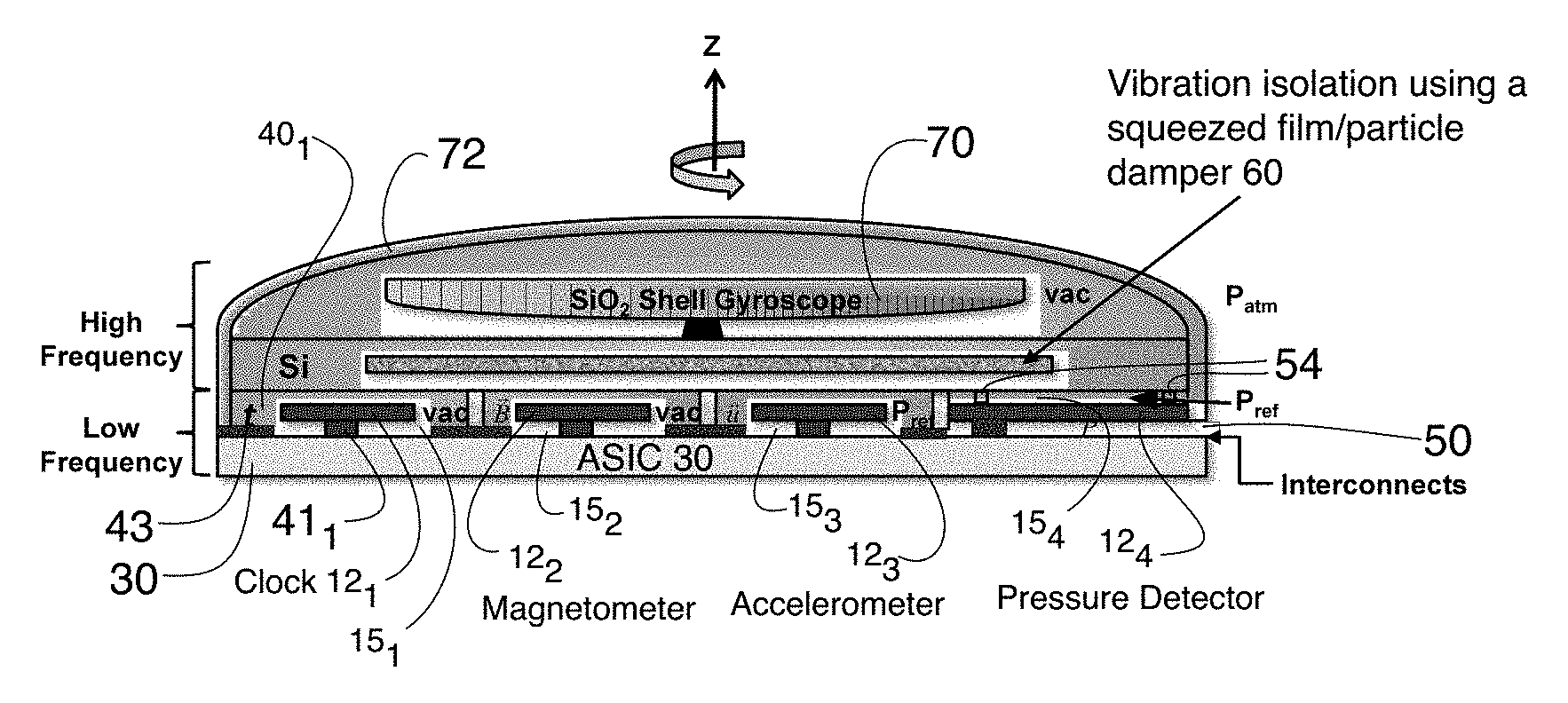
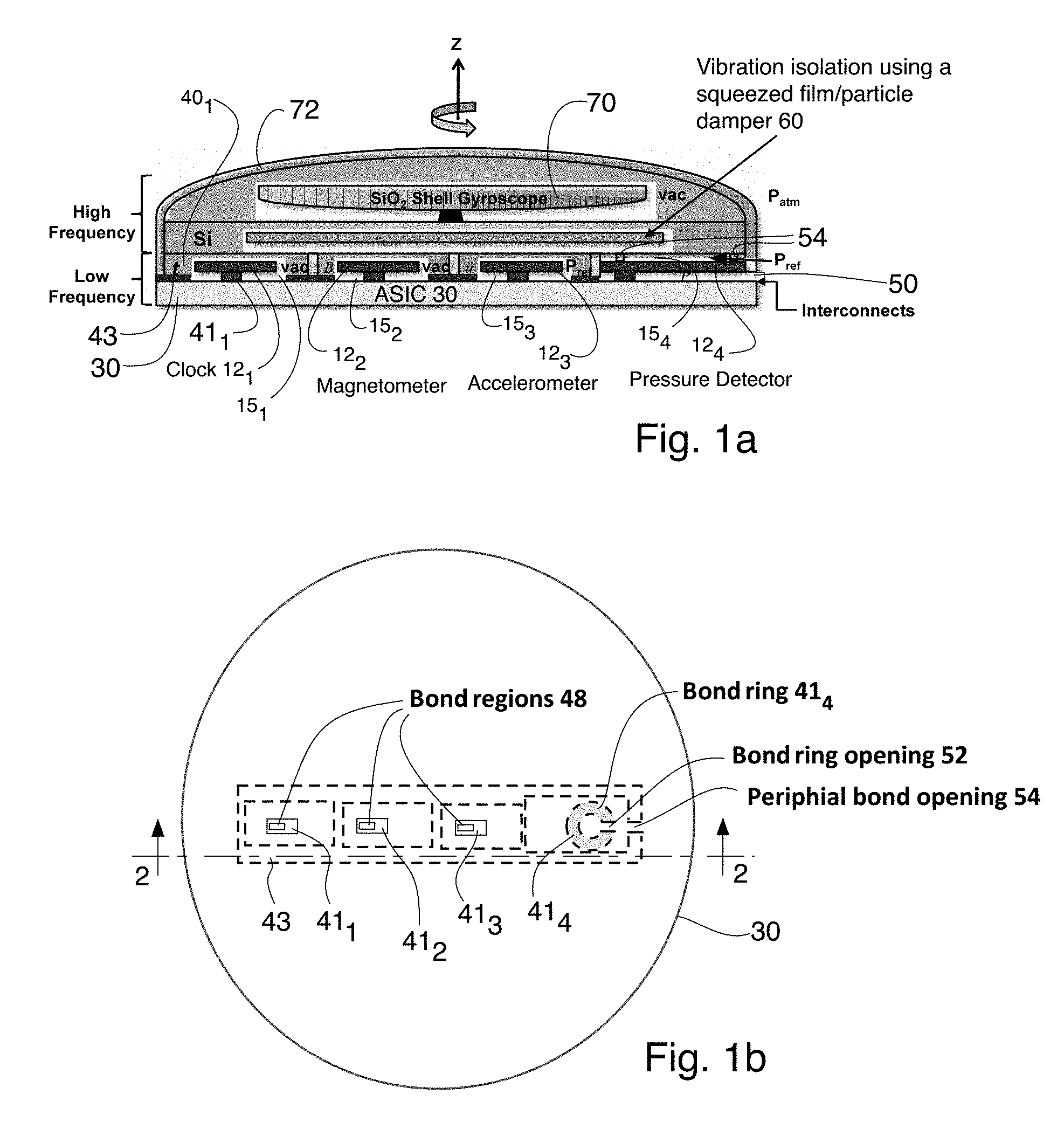
[0011] FIG. 1a is a side view schematic illustration of the monolithically formed INS showing sensor components sealed in individual environments and at specific required pressures, while FIG. 1b is a cross section view thereof.
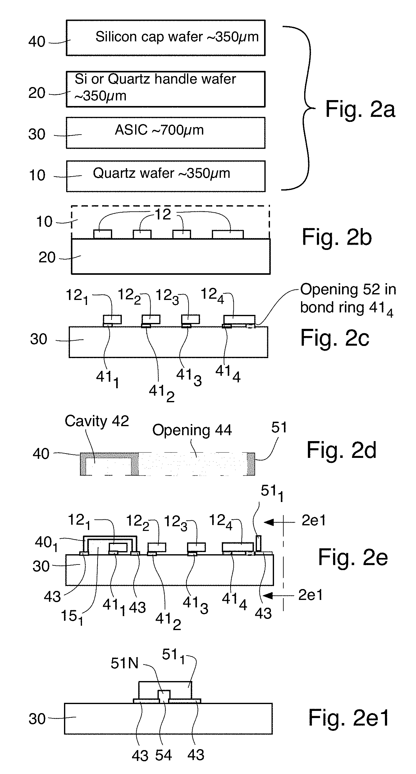
[0012] FIGS. 2a-2j are across view (taken along line 2-2 shown in FIG. 1b) showing the steps used in a method described herein to form a slightly modified embodiment of the monolithically formed INS depicted by FIG. 1a;
[0013] FIG. 2e1 is a side elevational view of the INS being formed at the step corresponding to FIG. 2e.
DETAILED DESCRIPTION
[0014] A schematic of the inertial navigation system (INS) is presented in FIG. 1a, in which components of the INS are preferably formed monolithically and then wafer bonded to enclose each sensor (or device) 12.sub.1-12.sub.4 of the INS in individual environments with individual cavities 15.sub.1-15.sub.4 using respective caps 40.sub.1-40.sub.4. In this way, the size of the composite unit is reduced and the alignment of the sensors (or devices) 12.sub.1-12.sub.4 within the system is also simplified since sensor alignment is achieved via lithographic wafer scale fabrication techniques and therefore post processing alignment can be eliminated. In order to discuss the construction of such an INS, the corresponding fabrication process flow is shown below in FIGS. 2a-2j. The sensors (or devices) are typically sensors (such as compasses, pressure detectors, magnetometers and/or accelerometers), but devices (such as electronic clocks) are sometimes also used in an INS and can be embodied in the INS using the same construction techniques as used with the sensors, as is described below.
[0015] Initially (see FIG. 2a) one begins with a quartz wafer 10, a quartz or silicon handle wafer 20, an Application Specific Integrated Circuit (ASIC) wafer 30 containing electronics and preferably as many silicon cap wafers 40.sub.1 . . . 40.sub.N as there are planned monolithic sensors 12.sub.1 . . . 12.sub.N to be formed from the quartz wafer 10. The embodiment of FIGS. 2a-2j has four sensors (or devices) three of which 12.sub.1 . . . 12.sub.3 are preferably totally encapsulated by an associated cap 40.sub.1 . . . 40.sub.3 in a hermetically sealed cavity 15.sub.1 . . . 15.sub.3 and one of which 12.sub.4 (a pressure detector) is partially encapsulated by cap 40.sub.4 and has an sealed cavity or pressure chamber 15.sub.4 associated with it for containing a gas at a reference pressure P.sub.ref. The pressure detector 12.sub.4 detects a differential pressure across a diaphragm, one side of which is exposed to that reference pressure P.sub.ref and the other side of which is preferably exposed to ambient pressure via a channel 50. The number and types of sensors and devices may be varied as needed to the use of any of them is optional.
[0016] The suggested initial thicknesses of these elements are identified on FIG. 2a but these thicknesses can be varied as needed or desired.
[0017] The quartz wafer 10 is temporarily bonded to the quartz or silicon handle wafer 20 (the quartz wafer 10 is shown in dashed lines in FIG. 2b) using a temporary adhesive, for example wax, (not shown) or a temporary fusion bond, followed by thinning and patterning of the quartz wafer 10 to define individual quartz sensors and/or devices 12 from quartz wafer 10 which are thus temporarily adhered to the quartz or silicon handle wafer 20 by the aforementioned temporary adhesive or fusion bond (or other temporary bonding technique). The individual quartz sensors and/or devices 12 of FIG. 2b are individually numbered 12.sub.1-12.sub.4 in the following figures. Four sensors and/or devices 12 are shown on FIG. 2b, but the number of sensors and/or devices 12 formed from the quartz wafer 10 may be varied as needed to accommodate the number needed in the sensor suite to be monolithically encapsulated.
[0018] Next the sensors and/or devices 12 are bonded to the ASIC wafer 30 at bond regions 41.sub.1-41.sub.3 and at a ring bond 41.sub.4 preferably using a thermo-compression bond under vacuum. The temporary quartz or silicon handle wafer 20 is then preferably removed resulting in the structure depicted by FIG. 2c. One of the sensors is preferably a pressure sensor to sense ambient pressure and therefor an opening 52 in the bond ring 41.sub.4 is provided to allow pressure equalization for the pressure sensor, which in this embodiment is sensor 12.sub.4. See FIG. 1b.
[0019] Recall that there are preferably a number of silicon cap wafers 40 which is preferably less than or equal to the number of sensors to be encapsulated. If two sensors both require the same ambient conditions then they may potentially share a common sealed cavity 15. In this embodiment four sensors are encapsulated individually and thus four silicon cap wafers 40 are utilized. Each of the cap wafers 40 is patterned with an appropriate cavity 15 and appropriate opening(s) 44 to seal individual sensors in particular environments needed by the individual sensor. FIG. 2d shows a cap wafer 40 with a single cavity 15 and an opening 44 therein (located between the cavity 15 and an end wall 51) positioned so that when this particular cap wafer 40 is applied to the structure depicted by FIG. 2c, the cavity 15 therein will cover and seal the left most sensor (or device) 12.sub.1 shown in FIG. 2c and leave the remaining sensors (or devices) 12.sub.2-12.sub.4 exposed through opening 44. Cavities 15 define the sealing environment (encapsulation) for typically a single sensor (or device) as each successive patterned cap wafer 40 is bonded into position on the ASIC wafer 30. The openings or holes 44 allow for a different environment when encapsulating of the other devices or sensors 12. The first sensor (or device) 12.sub.1 (a quartz clock, for example, in the embodiment of FIG. 1a) is sealed at some desired gas pressure P.sub.1 in a desired gas G.sub.1 through the bonding of the first patterned cap wafer 40.sub.1 to the ASIC wafer 30 at bond 43 forming the hermetically sealed cavity 15.sub.1 as shown in FIG. 2e.
[0020] In FIG. 2e the height of the bond regions 41.sub.1-41.sub.4 for the four sensors (or devices) 12.sub.1-12.sub.4 in this embodiment and the height of the peripheral bond region 43 for the four cap wafers 40.sub.1-40.sub.4 in this embodiment are exaggerated for ease of illustration. The peripheral bond region 43 is also shown in FIG. 1b by dashed lines. The peripheral bond region 43 preferably completely encircles each of the four sensors or devices 12.sub.1-12.sub.4 except the last one (12.sub.4) which is a preferably an ambient pressure detector and therefor needs a path 50 to ambient air. Therefore the pressure detector 12.sub.4 is only partially encircled by the peripheral bond region 43 in that there is preferably a break or opening in bond region 43 labeled by numeral 54. The end walls 51 of the four cap wafers 40.sub.1-40.sub.4 each also preferably has an opening or notch 51N therein to provide the path 50 to ambient air from sensor 12.sub.4 through opening 52 and through the openings 54 and/or notches 51N.
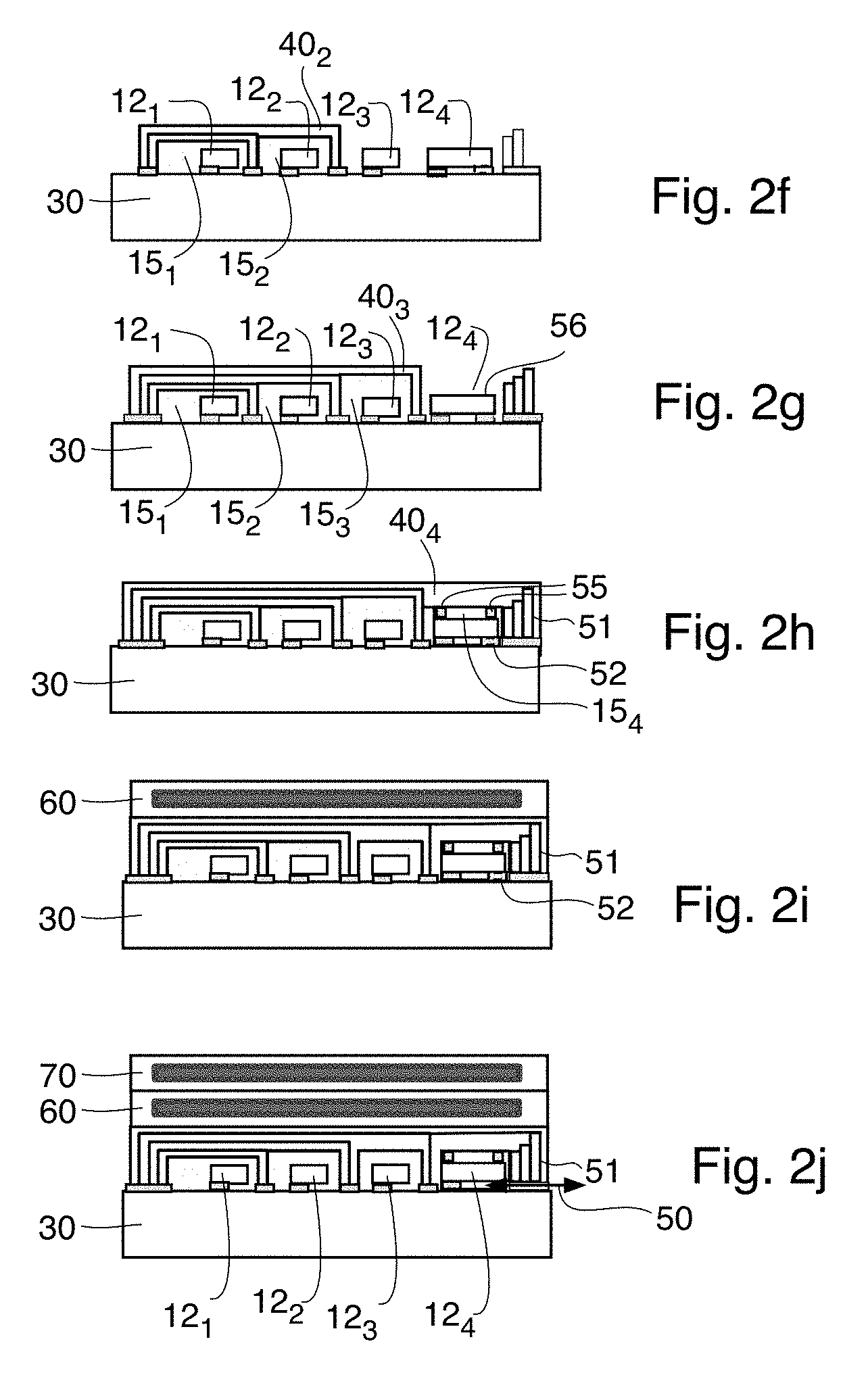
[0021] After the first sensor (or device) 12.sub.1 encapsulated within its cavity of cap wafer 40.sub.1, the second sensor 12.sub.2 (a quartz magnetometer, for example, in the embodiment of FIG. 1a) is then encapsulated at a gas pressure P.sub.2 in ambient gas G.sub.2 with the second patterned cap wafer 40.sub.2 at the peripheral bond 43 as shown in FIG. 2f. This process with successive cap wafers 40 (each with suitable cavities 15 and openings 44 defined therein) continues with the remaining sensors and cap wafers at their required environmental conditions being encapsulated preferably as shown by FIGS. 2g and 2h and bonded to layer 30 at, for example, bond the peripheral bond 43. The encapsulated pressure (P.sub.1, P.sub.2, etc.) may be 0, i.e., a vacuum and the gases G.sub.1, and G.sub.2, etc., if used, are preferably nitrogen and/or helium. The same gas (or a common vacuum) be used in two different encapsulations. So each encapsulated environment may have its own unique gas type and pressure, but, if desired, neighboring sensors or devices can share a unique gas type and pressure if desired.
[0022] In FIGS. 2f-2h each cap wafer 40 not only encapsulates a single sensor (or device) 12 with a desired gas at a desired pressure, but also re-encapsulates the previously encapsulated sensors (or devices) 12. Instead of having each successive cap wafer 40 re-encapsulate prior encapsulation(s), each successive cap wafer 40 may be formed instead to encapsulate only its associated sensor without also encapsulating any previous encapsulations as shown in FIG. 1a. Of course, various combinations of these two encapsulation techniques will suggest themselves to those skilled in the art.
[0023] The bonds 41.sub.1-41.sub.4 and 43 are preferably formed as a thermo-compression metal bond but other bond techniques could alternatively be used especially if the bonds need to be made at lower than usual temperatures for thermo-compression bonding due to, for example, a temperature sensitivity of one or more of the sensors. The stoichiometry of the bonds 43 for each of the cap wafers 40 is preferably selected to achieve a hermetic seal of the encapsulated sensors 12.sub.1-12.sub.3 within cavities 15.
[0024] The fourth device 12.sub.4 in this embodiment is preferably a pressure sensor which has a diaphragm 56 (see FIG. 2g) which is sealed around its perimeter by a perimeter seal 55 from above to define the cavity or chamber 15.sub.4 which preferably formed at the reference pressure of P.sub.ref. Below the diaphragm 56 is located a air path 50 (see also FIG. 2e1) to ambient in the form of the missing segment 52 of the bond metal ring 41.sub.4 and the missing portion 54 in the peripheral bond 43 in combination with opening(s) and/or notch(es) 51N allows equalization of the pressure under the diaphragm 56 with the ambient pressure to be measured via the air path 50.
[0025] The pressure sensor 12.sub.4 of this embodiment measures a differential pressure difference across diaphragm 56. On one side of the diaphragm 56, the pressure is well defined (at a reference pressure P.sub.ref) by the capping process of cap wafer 40.sub.4 under a controlled environment (gas and pressure) at seals 54. Alternatively, the damping unit 60 may be used as the final cap (see FIG. 1a). The final cap wafer 40.sub.4 in the embodiment of FIG. 2h utilizes a seal 54 at the edge of the cavity 15.sub.4 thereby locking in that controlled environment between the diaphragm 56 and the cap. On the other side of the diaphragm 56, the gap or opening 52 in the seal ring 41.sub.4 allows pressure to equalize to ambient pressure (via passage 50), which is the pressure to be measured.
[0026] Vibration isolation is desirable for many sensors and therefore a silicon wafer containing a vibration damping unit 60 is preferably bonded (see FIG. 2i) to the topmost cap 40 of the capped wafer stack shown in FIG. 2h. The vibration damping unit 60 may utilize a squeezed film or particles as the damping agent. The final component is preferably a gyroscope 70 which is bonded to the top of the vibration damping unit 60 (see FIG. 2j) to complete the encapsulation of the inertial navigation system. The vibration damping unit 60 is preferably bonded to the composite unit depicted in FIG. 2h providing a vibration-damped surface for receiving the gyroscope 70. The gyroscope 70 is mounted on the vibration damping unit 60. The vibration damping unit 60 may be fabricated using standard MEMS fabrications techniques. Preferred materials for the composite unit include semiconductors (silicon, etc.), dielectrics (silicon dioxide, silicon nitride, etc.), metals (aluminum, gold, titanium, etc) and polymers (polyamide, etc.).
[0027] The vibration damping unit 60 in some embodiments may be located under the ASIC wafer 30 (as viewed in FIG. 1a) instead of (or in addition to) on top of the encapsulated sensors 12 if none of the sensors is an accelerometer, for example.
[0028] The gyroscope 70, the damper 60 and the sensors 12 may be all enclosed within a rounded shell 72 as depicted by FIG. 1a if desired. Of course, the shell 72 may assume some other geometric shape (square, rectangular, etc.).
[0029] As can be seen with reference to FIG. 1a, sensor or device 12.sub.1 may serve as a resonator for a clock, while sensor or device 12.sub.2 may be magnetometer while sensor or device 12.sub.3 may be an accelerometer in order to form an INS as mentioned above. The sensors and devices 12.sub.1-12.sub.4 may perform other or additional tasks if desired.
[0030] This method may utilize quartz processing techniques described in U.S. Pat. No. 7,237,315 to make quartz based sensors 12.
[0031] This concludes the description of embodiments of the present invention. The foregoing description of these embodiments and methods of making same have been presented for the purposes of illustration and description. It is not intended to be exhaustive or to limit the invention to the precise form or methods disclosed. Many modifications and variations are possible in light of the above teachings. It is intended that the scope of the invention be limited not by this detailed description, but rather by the claims appended hereto.
* * * * *
D00000
D00001
D00002
D00003
XML
uspto.report is an independent third-party trademark research tool that is not affiliated, endorsed, or sponsored by the United States Patent and Trademark Office (USPTO) or any other governmental organization. The information provided by uspto.report is based on publicly available data at the time of writing and is intended for informational purposes only.
While we strive to provide accurate and up-to-date information, we do not guarantee the accuracy, completeness, reliability, or suitability of the information displayed on this site. The use of this site is at your own risk. Any reliance you place on such information is therefore strictly at your own risk.
All official trademark data, including owner information, should be verified by visiting the official USPTO website at www.uspto.gov. This site is not intended to replace professional legal advice and should not be used as a substitute for consulting with a legal professional who is knowledgeable about trademark law.