High Performance Multi-Component Electronics Power Module
Lam; Man Kit
U.S. patent application number 16/058782 was filed with the patent office on 2019-10-10 for high performance multi-component electronics power module. This patent application is currently assigned to Microchip Technology Incorporated. The applicant listed for this patent is Microchip Technology Incorporated. Invention is credited to Man Kit Lam.
| Application Number | 20190311977 16/058782 |
| Document ID | / |
| Family ID | 68097379 |
| Filed Date | 2019-10-10 |


View All Diagrams
| United States Patent Application | 20190311977 |
| Kind Code | A1 |
| Lam; Man Kit | October 10, 2019 |
High Performance Multi-Component Electronics Power Module
Abstract
Methods are provided for forming an IC power package including a power MOSFET device, a microprocessor/driver, and/or other discrete electronics. A lead frame may be etched to form a half-etch lead frame defining component attach structures at the top side of the lead frame. A power MOSFET may be mounted to a die attach pad defined in the half-etch lead frame, and the structure may be overmolded. The top of the overmolded structure may be grinded to reduce a thickness of the power MOSFET and expose a top surface of the MOSFET through the surrounding mold compound. A conductive contact may be formed on a top surface of the MOSFET. Selected portions of the half-etch lead frame may be etched from the bottom-up to separate the MOSFET from other package components, and to define a plurality of package posts for solder-mounting the package to a PCB.
| Inventors: | Lam; Man Kit; (Colorado Springs, CO) | ||||||||||
| Applicant: |
|
||||||||||
|---|---|---|---|---|---|---|---|---|---|---|---|
| Assignee: | Microchip Technology
Incorporated Chandler AZ |
||||||||||
| Family ID: | 68097379 | ||||||||||
| Appl. No.: | 16/058782 | ||||||||||
| Filed: | August 8, 2018 |
Related U.S. Patent Documents
| Application Number | Filing Date | Patent Number | ||
|---|---|---|---|---|
| 62655449 | Apr 10, 2018 | |||
| Current U.S. Class: | 1/1 |
| Current CPC Class: | H01L 23/49589 20130101; H01L 24/82 20130101; H01L 23/49548 20130101; H01L 2924/0665 20130101; H01L 2924/00014 20130101; H01L 2924/00014 20130101; H01L 2924/014 20130101; H01L 2224/13147 20130101; H01L 24/73 20130101; H01L 2224/131 20130101; H01L 2224/32245 20130101; H01L 21/4828 20130101; H01L 2224/2919 20130101; H01L 2924/00014 20130101; H01L 2924/014 20130101; H01L 2224/48175 20130101; H01L 24/24 20130101; H01L 24/32 20130101; H01L 21/4825 20130101; H01L 24/48 20130101; H01L 2224/13147 20130101; H01L 23/49582 20130101; H01L 23/3107 20130101; H01L 2224/48249 20130101; H01L 2224/24245 20130101; H01L 23/49513 20130101; H01L 23/49562 20130101; H01L 2224/291 20130101; H01L 2224/73265 20130101; H01L 24/00 20130101; H01L 23/49575 20130101; H01L 2224/24105 20130101; H01L 23/4952 20130101; H01L 23/49568 20130101; H01L 25/16 20130101; H01L 21/4832 20130101; H01L 2224/131 20130101; H01L 23/49524 20130101; H01L 21/565 20130101; H01L 2224/291 20130101; H01L 24/16 20130101; H01L 2224/2919 20130101; H01L 2924/18161 20130101; H01L 2224/16258 20130101; H01L 2224/32238 20130101; H01L 25/50 20130101; H01L 21/56 20130101 |
| International Class: | H01L 23/495 20060101 H01L023/495; H01L 23/31 20060101 H01L023/31; H01L 21/48 20060101 H01L021/48; H01L 21/56 20060101 H01L021/56 |
Claims
1. A power integrated circuit (IC) package, comprising: a half-etch lead frame; a power IC device mounted to the half-etch lead frame; wherein a front side of the power IC device is mounted to the half-etch lead frame in a face-down configuration; wherein a back side of the power IC device is ground down to define a reduced thickness of the power IC component; and a conductive ground contact formed on the ground down back side of the power IC device.
2. The power IC package of claim 1, further comprising a microcontroller flip-chip mounted to the half-etch lead frame.
3. The power IC package of claim 1, wherein the power IC device is configured to high operational currents, e.g., at least 1 A, at least 5 A, at least 10 A, or at least 20 A.
4. The power IC package of claim 1, wherein the power IC device comprises a power MOSFET (metal-oxide-semiconductor field-effect transistor).
5. The power IC package of claim 1, comprising a plurality of power IC devices mounted to the half-etch lead frame.
6. The power IC package of claim 1, including at least one solder wettable package post defined by portions of the half-etch lead frame, each solder wettable package post having a solder wettable bottom surface and at least one solder wettable side surface.
7. The power IC package of claim 1, wherein, the power IC device is structurally connected to at least one other IC component by a region of mold compound in an area in which a complete thickness of the lead frame is removed.
8. A method, comprising: forming a power integrated circuit (IC) package by a process including: etching a top side of a lead frame to define a half-etch lead frame defining one or more component attach structures; solder mounting a power IC device to at least one of the component attach structures; forming a mold compound over power IC device and half-etch lead frame to define an over-molded structure; performing a grind process on a top side of the over-molded structure to reduce a thickness of the power IC device and to expose a top surface of the power IC device through the mold compound; forming a conductive contact over the power IC device; and removing portions of the half-etch lead frame, from a bottom side of the half-etch lead frame, to physically separate selected portions of the half-etch lead frame.
9. The method of claim 8, further comprising mounting a bottom side of the power IC package to a printed circuit board.
10. The method of claim 8, wherein the step of removing portions of the half-etch lead frame, from a bottom side of the half-etch lead frame, defines at least one package post extending from a bottom side of the IC package; the method further comprises solder mounting the bottom side of the power IC package to a printed circuit board via the one or more package posts.
11. The method of claim 8, wherein the step of removing portions of the half-etch lead frame, from a bottom side of the half-etch lead frame, defines a plurality of package posts extending from a bottom side of the IC package; and the method further comprises: plating a bottom surface and at least one lateral side surface of each package post to define a plurality of solder wettable package posts; and solder mounting the power IC package to a printed circuit board via the plurality of solder wettable package posts.
12. The method of claim 8, wherein the process or forming the power IC package further comprises flip-chip mounting a microcontroller to at least one component attach structure at the top side of the half-etch lead frame.
13. The method of claim 8, wherein the power IC device comprises a power MOSFET (metal-oxide-semiconductor field-effect transistor).
14. The method of claim 8, wherein solder mounting the plurality of IC components to the component attach structures at the top side of the lead frame comprises mounting a plurality of power IC devices to the lead frame.
15. The method of claim 8, wherein the process of forming the power IC device does not include a Taiko.TM. thin-grind process.
16. The method of claim 8, wherein the power IC device is solder mounted to the lead frame without applying a back metal to the power IC device prior to the solder mounting.
17. A method, comprising: forming a power integrated circuit (IC) package by a process including: etching a top side of a lead frame to define a half-etch lead frame defining a die attach pad and a plurality of wire bond posts; mounting a power IC device to the die attach pad; forming wire bonds to connect the power IC device with the plurality of wire bond posts; forming a mold compound over power IC device, wire bond posts, and wire bonds to define an over-molded structure; and removing portions of the half-etch lead frame, from a bottom side of the half-etch lead frame, to separate the die attach pad from the plurality of wire bond posts.
18. The method of claim 17, further comprising mounting a bottom side of the power IC package to a printed circuit board.
19. The method of claim 17, wherein the step of removing portions of the half-etch lead frame, from a bottom side of the half-etch lead frame, defines a plurality of package posts extending from a bottom side of the IC package; and the method further comprises: plating a bottom surface and at least one lateral side surface of each package post to define a plurality of solder wettable package posts; and solder mounting the power IC package to a printed circuit board via the solder wettable package posts.
20. The method of claim 17, wherein the power IC device comprises a MOSFET (metal-oxide-semiconductor field-effect transistor) QFN (quad-flat no-leads) device.
Description
RELATED PATENT APPLICATION
[0001] This application claims priority to U.S. Provisional Patent Application No. 62/655,449 filed Apr. 10, 2018, the entire contents of which are hereby incorporated by reference for all purposes.
TECHNICAL FIELD
[0002] The present disclosure relates to electronics packages, and more particularly, a multi-component electronics package module having high performance characteristics, e.g., high current operation with efficient heat dissipation.
BACKGROUND
[0003] In typical power IC packages, e.g., MOSFET devices, in order to improve device performance, high current may need to be applied to the device to help lower the RDS(on) (Drain-Source on resistance). One technique to address this is to apply multiple wire bonds to connect the Source to the package lead frame. However, the wire resistance and contact resistances limit the effectiveness of such design. Another technique is solder attach a discrete copper clip onto the package lead frame to connect it to the MOSFET Source terminal. However, this solution adds cost.
[0004] FIG. 1A is a bottom view of an example conventional MOSFET DFN (dual-flat no-leads) package 10, indicating source, drain, and gate contacts on the bottom side of the package. FIG. 1B is a top view of the MOSFET package 10 during fabrication. Package 10 includes a lead frame 20 including a die-attach pad (DAP) 22 and a plurality of lead fingers 24. A MOSFET die 12 is mounted to the DAP 22, e.g., by solder, epoxy, etc. A copper clip 30 is solder attached to the MOSFET die and then to lead frame 20.
[0005] Another common issue is thermal management in the power IC package. In the above described solutions, the bottom side of the MOSFET device is solder attached onto the lead frame DAP. This typically requires a back-metal deposition step. In order to reduce RDS(on), the MOSFET die may need to be ground thin (e.g., .about.50 um), for example using the Taiko.TM. thin-grind process, followed by a Ti--Ni--Ag backmetal deposition for die attach.
SUMMARY
[0006] Embodiments of the present disclosure provide methods of forming IC power packages, and IC power packages formed using such methods. Some embodiments provide power MOSFET packages, e.g., including a MOSFET device, a microprocessor/driver, and/or one or more other discrete electronic components assembled in a DFN or QFN. In some embodiments, a power IC package is formed without needing an expensive back-grind, e.g., the Taiko.TM. back-grind process, and without a back-metal deposition process. In addition, the package may be formed without a copper clip. Further, in some embodiments, the power package includes a plurality of wettable package posts for solder-mounting the package to a PCB or other structure.
[0007] One embodiment provides a method of forming a power integrated circuit (IC) DFN package including a power IC device, e.g., a power MOSFET. A top side a lead frame may be etched to form a half-etch lead frame defining component attach structures at the top side of the lead frame. A power IC device, e.g., power MOSFET, may be solder mounted to at least one of the component attach structures. The structure may then be overmolded. A grind process may be performed on the top side of the overmolded structure to reduce a thickness of the power IC device and to expose a top surface of the power IC device through the mold compound. A conductive contact may then be formed over and in contact with the power IC device. Selected portions of the half-etch lead frame may then be etched from the bottom side of the structure, to separate the power IC device from other components or structures in the package. The bottom-up etch may also define a plurality of package posts extending from the bottom the IC package. The package posts may be plated to increase the wettability of the posts, such that the package may be solder mounted to a PCB or other structure via the wettable package posts.
[0008] Another embodiment provides another method of forming a power integrated circuit (IC) package including a power IC device, e.g., a power MOSFET QFN. A top side of a lead frame may be half-etch to define a half-etch lead frame defining a die attach pad and a plurality of wire bond posts. A power IC device, e.g., a power MOSFET QFN, may be mounted to the die attach pad, e.g., by epoxy, and wire bonds may be connected between the power IC device and the wire bond posts. The structure may then be overmolded. Portions of the half-etch lead frame may then be etched from the bottom side of the structure, to thereby separate the die attach pad from the wire bond posts. The bottom-up etch may also define a plurality of package posts extending from the bottom the IC package. The package posts may be plated to increase the wettability of the posts, such that the package may be solder mounted to a PCB or other structure via the wettable package posts.
BRIEF DESCRIPTION OF THE DRAWINGS
[0009] Example aspects of the present disclosure are described below in conjunction with the figures, in which:
[0010] FIGS. 1A and 1B illustrate an example conventional MOSFET DFN (dual-flat no-leads) package;
[0011] FIG. 2 illustrates a cross-section of an example power IC package including a power MOSFET DFN and MCU/driver, according to one embodiment of the invention;
[0012] FIGS. 3A-3J illustrate an example method of forming the example power IC package shown in FIG. 2, according to one example embodiment of the invention;
[0013] FIG. 4 illustrates a cross-section of an example power module including a MOSFET DFN with wettable flank, according to another embodiment of the invention;
[0014] FIGS. 5A-5F shows an example process for forming an example wettable-flank MOSFET QFN package, according to another embodiment of the invention;
[0015] FIG. 6A illustrates and example power package shown in shown in FIGS. 2 and 3J surface mounted to a PCB via wettable posts of the power package; and
[0016] FIG. 6B illustrates and example power package shown in shown in FIGS. 2 and 3J through-hole mounted to a PCB via wettable posts of the power package.
DETAILED DESCRIPTION
[0017] Embodiments of the present disclosure provide methods of forming an integrated circuit (IC) power package and IC power packages formed using such methods.
[0018] FIG. 2 illustrates a cross-section of an example power IC package 100, specifically a power module including a power MOSFET DFN and MCU/driver, according to an example embodiment of the present invention. The power IC package 100 may include a plurality of IC components mounted to a half-etch lead frame, which is further processed to form the illustrated package that can be solder mounted to a printed circuit board (PCB), as shown in FIG. 4. Remaining portions of the half-etch lead frame, after completion of the package fabrication (during which selected portions of the half-etch lead frame are removed), are indicated at 102, and referred to below as half-etch lead frame 102.
[0019] In this embodiment, the plurality of IC components include a thin (e.g., .about.50 .mu.m) power MOSFET 104 front-side-mounted to the half-etch lead frame 102, a microcontroller (MCU)/driver 106 flip-chip mounted to the half-etch lead frame 102, and one or more discrete IC elements 108 (e.g., one or more inductor, capacitor, ASIC, memory device, etc.) mounted to the half-etch lead frame 102. MOSFET 104 and MCU 106 may be mounted to half-etch lead frame 102 by solder connections 110.
[0020] In this embodiment, after mounting the MOSFET 104 and MCU 106 and performing an overmold using a mold compound 112, the back side of the power MOSFET 104 and MCU 106 (the top sides shown in FIG. 2) may be ground down to a desired thickness, which also exposes the back sides of the MOSFET 104 and MCU 106 through the mold compound, and conductive (e.g., copper) contacts 116 are then deposited on the exposed, ground down back sides of the MOSFET 104 and MCU 106, e.g., for ground connection to the MOSFET 104. The back (bottom) side of the power IC package may be formed to define a plurality of solder wettable package posts 120 (e.g., defined by portions of the half-etch lead frame 102), for solder mounting the package to a PCB, as shown in FIG. 4. Posts 120 may be covered by an electroless plating layer 122. As shown, each 120 post may have an exposed solder-wettable bottom surface and at least one exposed solder-wettable side surface, which may allow for improved solder connection to the PCB and improved inspection of the solder connections.
[0021] The face-down configuration of the power MOSFET 104 allows high current to be applied to the MOSFET source. Further, as discussed above, by grinding the MOSFET die 104 after overmolding the package, metal (e.g., copper) 116 can be deposited on the exposed back side of the MOSFET 104, e.g., for ground connection. This negates the need to employ the expensive Taiko.TM. back-grind and back-metal (e.g., Ti--Ni--Ag back metal) deposition process. Further, the top side of the power IC package 100 may be pattern-plated to incorporate pads for discretes 108 and interconnect traces into the package product.
[0022] In addition, power IC package 100 may avoid the need for a copper clip as used in conventional packages. Further, power IC package 100 may be independent of wafer size and material. In addition, power IC package 100 may be strip testable, to allow testing of individual or defined groups of packages, as opposed to conventional designs.
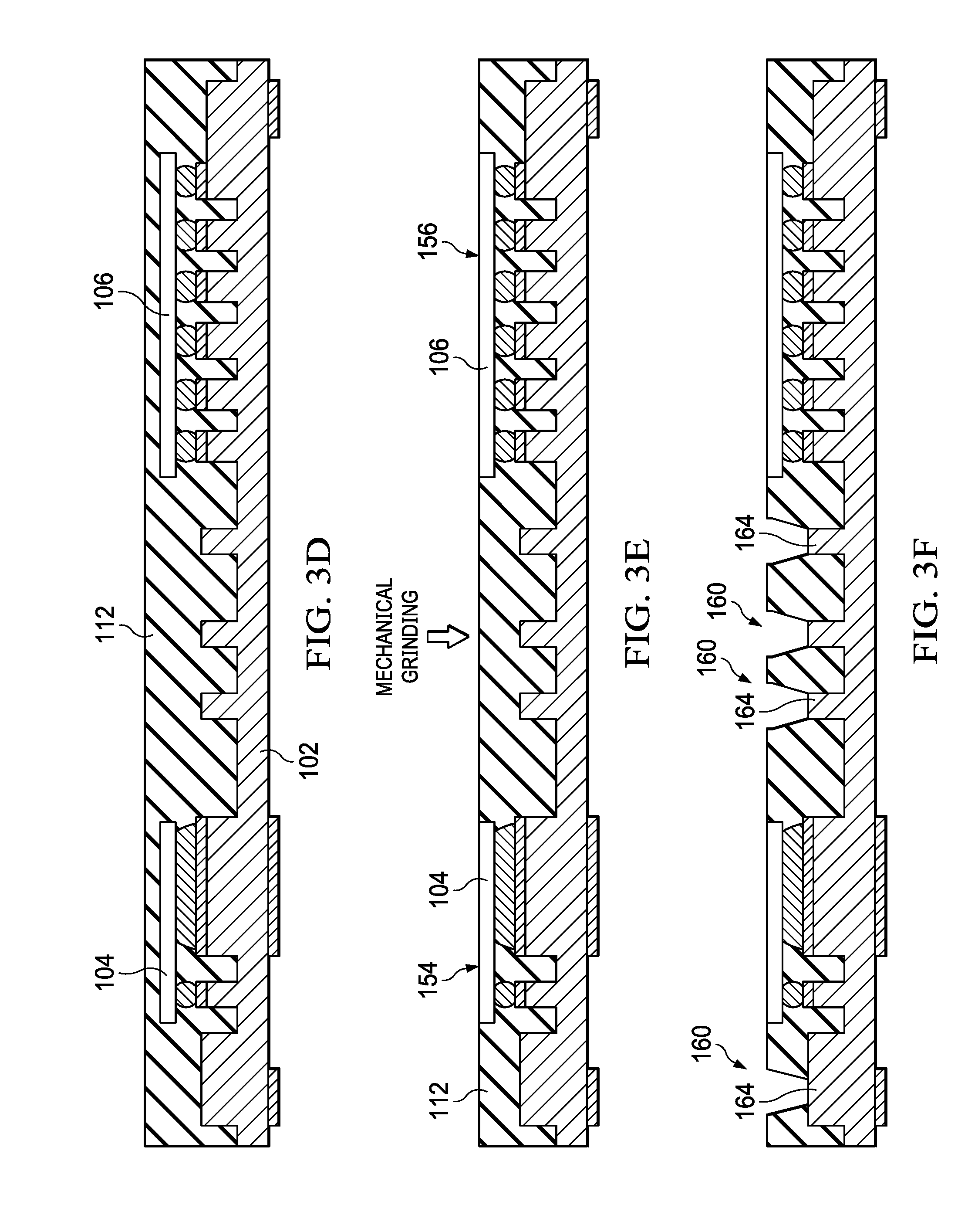
[0023] FIGS. 3A-3J illustrate an example method of forming the example power IC package 100 shown in FIG. 2 (power module including a power MOSFET DFN and MCU/driver), according to one example embodiment of the present invention.
[0024] As shown in FIG. 3A, a copper alloy lead frame strip 100 may be provided.
[0025] As shown in FIG. 3B, the lead frame strip 140 may be patterned and "half-etch" on the top side. For example, the top and bottom sides may be pattern-plated to deposit a solderable metal layer 142 (e.g., Sn, Sn alloy, Ag, Ni--Pd--Au, Ni--Au, etc.) having resistance to Cu etching chemistry, and a Cu half-etch may then be performed to remove portions of the lead frame strip 100, thereby defining a half-etch lead frame 102. As shown, the resulting structure defines a number of plated attach pads/posts 146.
[0026] As shown in FIG. 3C, the front sides of a power MOSFET 104 and a microcontroller/driver 106 (flip-chip mounted) may be reflow-attached to respective plated attach pads/posts 146 defined by the half-etch lead frame using Cu pillar bumps or solder bumps 150.
[0027] As shown in FIG. 3D, the structure may be over-molded using any suitable mold compound 112.
[0028] As shown in FIG. 3E, a mechanical grinding process may be performed on the top side of the structure to remove an upper thickness of mold compound 112. In some embodiments, the mechanical grinding may extend down into the MOSFET 104 and MCU 106, to thereby reduce a respective thickness of MOSFET 104 and MCU 106, and expose a back side 154 of MOSFET 104 and back side 156 of MCU 106 through the removed portions of the mold compound 112.
[0029] As shown in FIG. 3F, a number of openings may be formed, e.g., laser drilled, through the mold compound 112 to define via openings 160 at respective metal posts 164 (e.g., not covered by plating 142) of the lead frame 102.
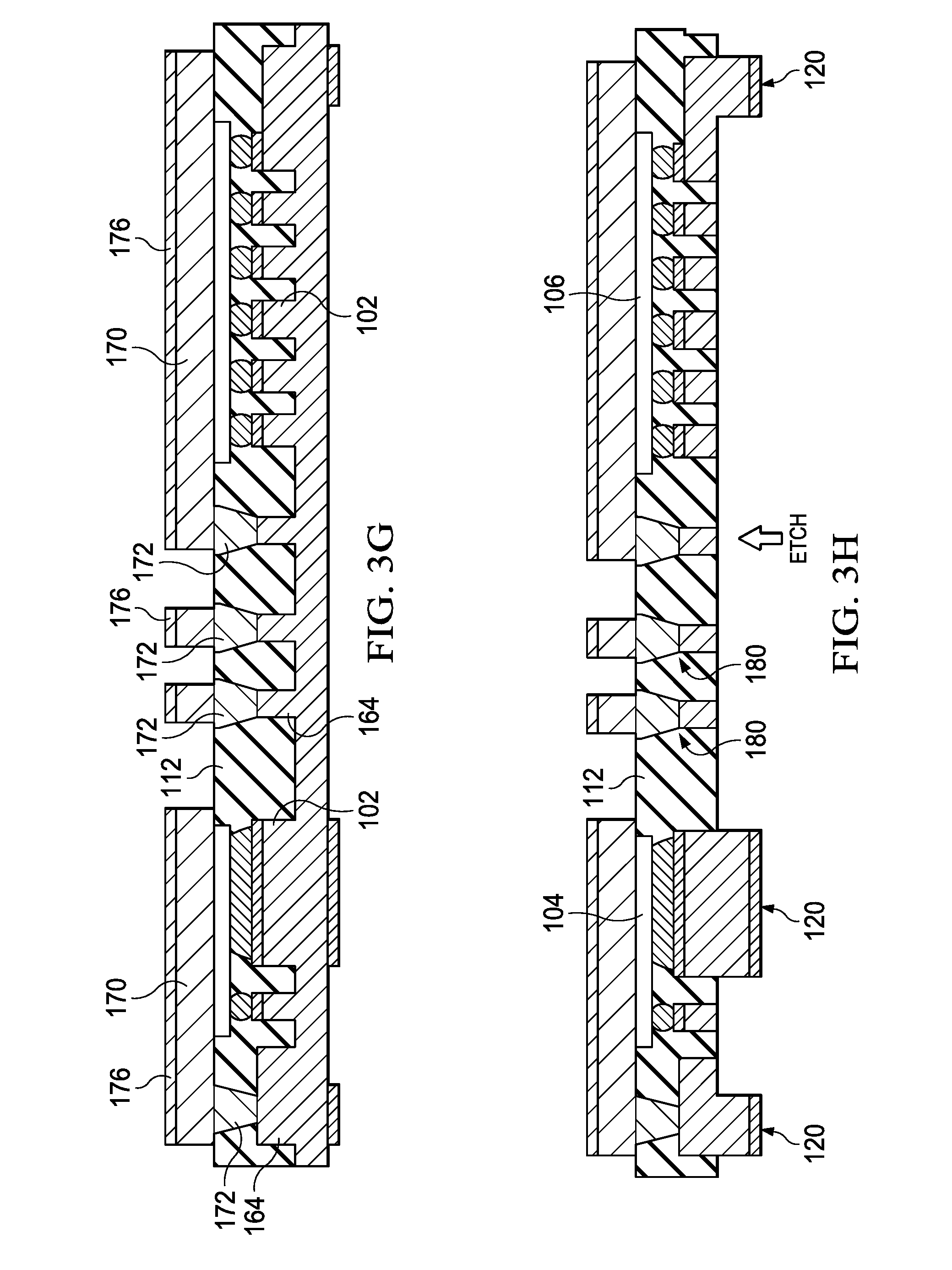
[0030] As shown in FIG. 3G, a thick copper layer cap metal 170 may be deposited onto the exposed top surface of the mold compound and semiconductor devices (MOSFET and MCU), and extending down into the via openings 160 to define copper vias 172, followed by a patterned cap metal 176 over the copper layer 170, followed by a copper etch to remove portions of the copper layer 170 unprotected by the pattered cap metal 176. The cap metal 176 may comprise Sn, Sn alloy, Ag, Ni--Pd--Au, Ni--Au, or other suitable metal that is minimally attacked by the Cu etching chemistry.
[0031] As shown in FIG. 3H, a Cu etch may be performed on the bottom of the package structure, in a bottom-up direction, to the mold compound 112. As shown, this etch may electrically/conductively separate the various IC components from each other, e.g., MOSFET 104, MCU 106, and copper structures 180 (comprising selected metal posts 164 connected to copper vias 172) for subsequently mounting one or more discretes 108 (shown in FIG. 2). This bottom-up etch may also define downwardly-extending package posts 120 for mounting the completed power IC package 100 to a PCB.
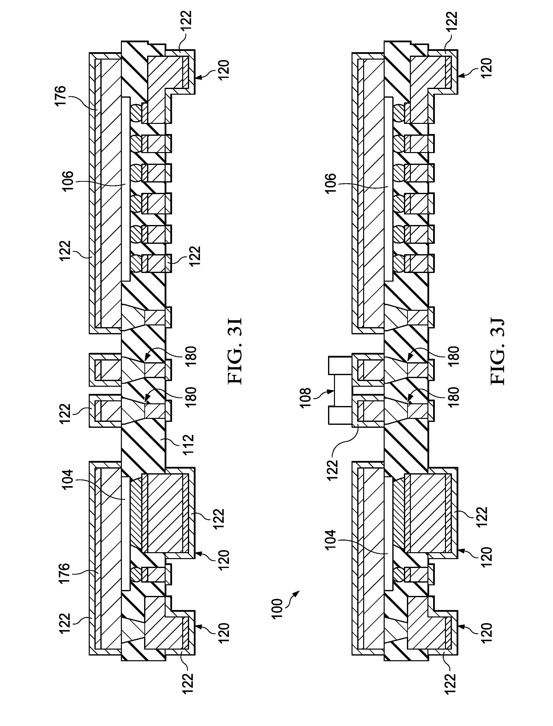
[0032] As shown in FIG. 3I, an electroless plating 122 may be deposited on exposed surfaces of the package, including exposed surfaces of package posts 120, to protect exposed surfaces from oxidation (including exposed copper surfaces and/or exposed surface of metal plating layer 142) and to improve the solder wettability of package posts 120 for mounting the package to a PCB or other structure. As shown, the electroless plating 122 may cover exposed bottom surfaces and exposed lateral side surfaces of package posts 120, e.g., to improve soldering of the package to a PCB or other structure (in some implementations, the solder material may flow onto one or more lateral side surfaces of the solder wettable package posts 120, as shown in FIGS. 6A and 6B discussed below). The electroless plating 122 may include Sn, Sn alloy, ENIG (electroless nickel immersion gold), ENEPIG (electroless nickel electroless palladium immersion gold), or any material(s) suitable to protect exposed metal surfaces from oxidation and/or promote soldering to a PCB or other structure.
[0033] In addition, the (plated) copper features at the top of the package structure may define component attach pads, interconnect traces, heat spreaders, etc. Thus, as shown in FIG. 3J, one or more capacitors 108 may be mounted to upper attach posts/pads 180. FIG. 3J thus shows the completed power IC package 100 shown in FIG. 2.
[0034] FIG. 4 illustrates a cross-section of an example power module 200, specifically a MOSFET DFN with wettable flank, according to an example embodiment of the present invention. Power module 200 may comprise the left-side portion of the power module 100 discussed above, and may be produced using the relevant steps shown in FIGS. 3A-3J. Thus, as shown, power module 200 may include a power MOSFET die 204 mounted as discussed above regarding MOSFET die 104, and one or more solder wettable package posts 220, e.g., having bottom and lateral sides covered by a solder wettable plating 222, e.g., as discussed above regarding wettable package posts 120.
[0035] FIGS. 6A-6F illustrate an example process for forming another example power IC package 300, in particular a strip-testable wettable-flank QFN (quad-flat no-leads) package, according to another example embodiment.
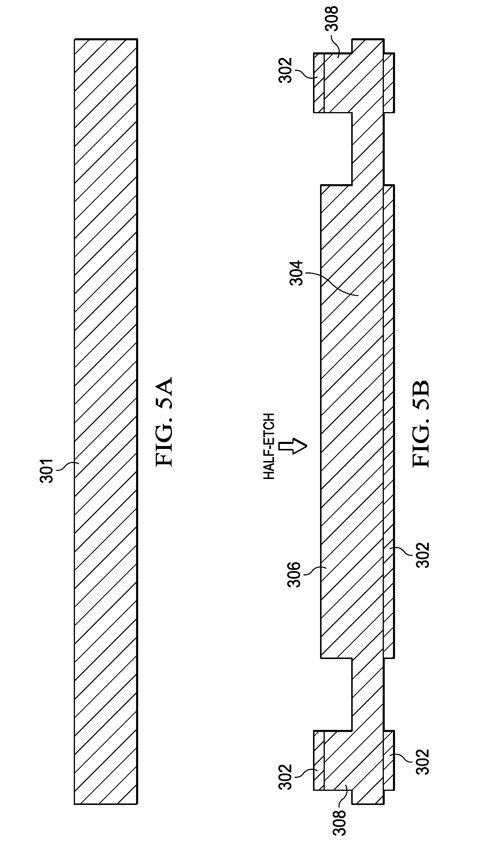
[0036] As shown in FIG. 5A, a copper alloy lead frame strip 301 may be provided.
[0037] As shown in FIG. 5B, the lead frame strip 301 may be patterned and "half-etch" on the top side. For example, the top and bottom sides may be pattern-plated to deposit a solderable metal layer 302 (e.g., Sn, Sn alloy, Ag, Ni--Pd--Au, Ni--Au, etc.) having resistance to Cu etching chemistry, and a Cu half-etch may then be performed to remove portions of the lead frame strip 301, thereby defining a half-etch lead frame 304. As shown, the resulting structure may define a number of plated or non-plated attach pads/posts, including an non-plated die attach pad 306 for mounting a MOSFET QFN and a plurality of plated attach posts 308 for wire bond connections to the mounted MOSFET QFN.
[0038] As shown in FIG. 5C, a power MOSFET QFN 312 may be mounted to die attach pad 306, e.g., via a deposited epoxy 310, and wire bonded to a plurality of plated attach posts 308.
[0039] As shown in FIG. 5D, the structure may be over-molded using any suitable mold compound 320.
[0040] As shown in FIG. 5E, a Cu etch may be performed on the bottom of the package structure, in a bottom-up direction, to remove portions of the half-etch lead frame 304 to thereby electrically/conductively separate the MOSFET die attach pad 306 from the lead posts 308, and to define a plurality of downwardly-extending package posts 324 for mounting the completed power IC package 300 to a PCB.
[0041] As shown in FIG. 5F, an electroless plating 330 may be deposited on exposed surfaces of the package, including exposed surfaces of package posts 324, to protect exposed surfaces from oxidation (including exposed copper surfaces and/or exposed surface of metal plating layer 330) and to improve the solder wettability of package posts 324 for mounting the package to a PCB or other structure. As shown, the electroless plating 330 may cover exposed bottom surfaces and exposed lateral side surfaces of package posts 324, e.g., to improve soldering of the package to a PCB or other structure (in some implementations, the solder material may flow onto one or more lateral side surfaces of the solder wettable package posts 120, as shown in FIGS. 6A and 6B discussed below). The electroless plating 330 may include Sn, Sn alloy, ENIG (electroless nickel immersion gold), ENEPIG (electroless nickel electroless palladium immersion gold), or any material(s) suitable to protect exposed metal surfaces from oxidation and/or promote soldering to a PCB or other structure.
[0042] As discussed above, a power package formed according to various embodiments, e.g., the example power packages shown in FIG. 2 (and similarly FIG. 3J), FIG. 4, and FIG. 5F, may include solder wettable package posts for mounting the respective power package to a PCB or other structure. Thus, FIGS. 6A and 6B illustrate example techniques for surface-mounting and through-hole mounting the example power IC package 100 shown in shown in FIGS. 2 and 3J to a PCB. The other example power packages disclosed herein, and any other power package formed according to the present invention, may be similarly mounted to a PCB or other structure.
[0043] First, FIG. 6A illustrates the example power IC package 100 (power module including a power MOSFET DFN and MCU/driver) shown in FIGS. 2 and 3J surface mounted to PCB 190, according to an example embodiment. As shown, the solder wettable posts 120 of power module 100 may be mounted to PCB 190 using a suitable solder material 192.
[0044] Second, FIG. 6B illustrates the example power IC package shown in FIGS. 2 and 3J through-hole mounted to PCB 190, according to an example embodiment. As shown, the solder wettable posts 120 of package 100 may be inserted through holes in PCB 190 and secured to PCB 190 using a suitable solder material 192.
* * * * *
D00000
D00001
D00002
D00003
D00004
D00005
D00006
D00007
D00008
D00009
D00010
D00011
XML
uspto.report is an independent third-party trademark research tool that is not affiliated, endorsed, or sponsored by the United States Patent and Trademark Office (USPTO) or any other governmental organization. The information provided by uspto.report is based on publicly available data at the time of writing and is intended for informational purposes only.
While we strive to provide accurate and up-to-date information, we do not guarantee the accuracy, completeness, reliability, or suitability of the information displayed on this site. The use of this site is at your own risk. Any reliance you place on such information is therefore strictly at your own risk.
All official trademark data, including owner information, should be verified by visiting the official USPTO website at www.uspto.gov. This site is not intended to replace professional legal advice and should not be used as a substitute for consulting with a legal professional who is knowledgeable about trademark law.