Substrate Processing Method
Choi; Seung Woo
U.S. patent application number 16/255639 was filed with the patent office on 2019-10-03 for substrate processing method. The applicant listed for this patent is ASM IP Holding B.V.. Invention is credited to Seung Woo Choi.
| Application Number | 20190304776 16/255639 |
| Document ID | / |
| Family ID | 68055462 |
| Filed Date | 2019-10-03 |


| United States Patent Application | 20190304776 |
| Kind Code | A1 |
| Choi; Seung Woo | October 3, 2019 |
SUBSTRATE PROCESSING METHOD
Abstract
A substrate processing method capable of uniformly maintaining damage to a pattern structure under a thin film formed on a substrate includes supplying a source material to a substrate on which a pattern structure that is reactive with a reactant is formed; and supplying the reactant through at least a central gas inlet of a supply unit in a plasma atmosphere, wherein, during the supplying of the reactant, a blocking material different from the reactant is supplied through an additional gas inlet that is spaced apart from the central gas inlet of the supply unit, and a flow of the blocking material at the edge of the substrate is increased, thereby increasing a radical density of the reactant near a center of the substrate.
| Inventors: | Choi; Seung Woo; (Cheonan-si, KR) | ||||||||||
| Applicant: |
|
||||||||||
|---|---|---|---|---|---|---|---|---|---|---|---|
| Family ID: | 68055462 | ||||||||||
| Appl. No.: | 16/255639 | ||||||||||
| Filed: | January 23, 2019 |
| Current U.S. Class: | 1/1 |
| Current CPC Class: | C23C 16/45542 20130101; C23C 16/45544 20130101; C23C 16/402 20130101; H01L 21/02164 20130101; H01L 21/31111 20130101; C23C 16/042 20130101; C23C 16/45502 20130101; C23C 16/50 20130101; C23C 16/04 20130101; C23C 16/45534 20130101; C23C 16/45574 20130101; H01L 21/0228 20130101; C23C 16/45565 20130101; H01L 21/02274 20130101; H01L 21/0337 20130101 |
| International Class: | H01L 21/02 20060101 H01L021/02; C23C 16/04 20060101 C23C016/04; C23C 16/40 20060101 C23C016/40; C23C 16/50 20060101 C23C016/50; H01L 21/311 20060101 H01L021/311; H01L 21/033 20060101 H01L021/033 |
Foreign Application Data
| Date | Code | Application Number |
|---|---|---|
| Mar 30, 2018 | KR | 10-2018-0037762 |
Claims
1. A substrate processing method comprising: supplying a first gas to a substrate on which a pattern structure is formed; purging the first gas; supplying a second gas and a third gas to form a thin film on the pattern structure in a plasma atmosphere, wherein the second gas is reactive with the first gas; and purging the second gas, wherein, during the forming of the thin film, the second gas is supplied through at least a central gas inlet of a gas supply unit, and the third gas is supplied through an additional gas inlet which is spaced apart from the central gas inlet of the gas supply unit, and the third gas is a gas different from the first gas and the second gas and has greater ionization energy than ionization energy of an inert gas.
2. The substrate processing method of claim 1, wherein, as the third gas is supplied through the additional gas inlet, a flow of the third gas at an edge of the substrate is increased, and thus a radical density near a center of the substrate is increased.
3. The substrate processing method of claim 2, wherein the third gas comprises a nitrogen component.
4. The substrate processing method of claim 3, wherein the third gas comprises at least one of a nitrous oxide gas and a nitrogen gas.
5. The substrate processing method of claim 1, wherein the second gas comprises an oxygen component and the third gas comprises a nitrogen component, and the thin film is an oxide film formed at a temperature of about 100.degree. C. or less.
6. The substrate processing method of claim 5, wherein the second gas is an oxygen gas and the third gas is a nitrous oxide gas, and a flow ratio of the oxygen gas to the nitrous oxide gas is 1:0.625 to 1:1.25.
7. The substrate processing method of claim 5, wherein the second gas is an oxygen gas and the third gas is a nitrogen gas, and a flow ratio of the oxygen gas and the nitrogen gas is 1:0.625 to 1:1.25.
8. The substrate processing method of claim 1, wherein damage to the pattern structure occurs in the plasma atmosphere.
9. The substrate processing method of claim 8, wherein the damage to the pattern structure is changed by the third gas supplied through the additional gas inlet.
10. The substrate processing method of claim 8, wherein the pattern structure comprises a spin-on hardmask (SOH).
11. The substrate processing method of claim 1, further comprising a double patterning process or a quadruple patterning process performed using the thin film formed on the pattern structure.
12. The substrate processing method of claim 1, wherein, in the plasma atmosphere, the second gas is ionized and the third gas is not ionized.
13. The substrate processing method of claim 1, wherein the first gas reacts with the second gas at a first temperature, and the first gas does not react with the third gas at the first temperature.
14. The substrate processing method of claim 1, wherein the third gas has greater ionization energy than ionization energy of the first gas and the second gas.
15. A substrate processing method comprising: supplying a silicon-containing gas to a substrate on which a pattern structure that is reactive with oxygen is formed; purging the silicon-containing gas; supplying an oxygen-containing gas and a nitrogen-containing gas in a plasma atmosphere at a temperature of about 100.degree. C. or less, and forming a silicon oxide film on the pattern structure; and purging the oxygen-containing gas, wherein, during the forming of the silicon oxide film, the oxygen-containing gas is supplied through at least a central gas inlet of a gas supply unit, and the nitrogen-containing gas is supplied through an additional gas inlet which is spaced apart from the central gas inlet of the gas supply unit.
16. The substrate processing method of claim 15, wherein the pattern structure that is reactive with oxygen radical is a spin-on hardmask, the oxygen-containing gas is an oxygen gas and the nitrogen-containing gas is a nitrous oxide gas, and a flow ratio of the oxygen gas to the nitrous oxide gas in the plasma atmosphere is 1:0.625 to 1:1.25.
17. The substrate processing method of claim 15, wherein, during the forming of the silicon oxide film, the silicon-containing gas adsorbed on the pattern structure of the substrate reacts with the oxygen-containing gas and does not react with the nitrogen-containing gas.
18. The substrate processing method of claim 15, wherein the nitrogen-containing gas is supplied through the additional gas inlet to increase a flow at an edge of the substrate, due to the increased flow of nitrogen-containing gas at the edge of the substrate, a density of a radical that is reactive with the pattern structure at the edge of the substrate is reduced, due to the increased flow of nitrogen-containing gas at the edge of the substrate, the density of a radical that is reactive with the pattern structure at a center of the substrate is increased, and damage to the pattern structure at the edge of the substrate and damage to the pattern structure near the center of the substrate become uniform.
19. A substrate processing method comprising: supplying a source material to a substrate on which a pattern structure that is reactive with a reactant is formed; and supplying the reactant through at least a central gas inlet of a supply unit in a plasma atmosphere, wherein, during the supplying of the reactant, a blocking material different from the reactant is supplied through an additional gas inlet that is spaced apart from the central gas inlet of the supply unit, and a flow of the blocking material at the edge of the substrate is increased, thereby increasing a radical density of the reactant near a center of the substrate.
20. The substrate processing method of claim 19, wherein the blocking material has greater ionization energy than ionization energy of an inert gas.
Description
CROSS-REFERENCE TO RELATED APPLICATION
[0001] This application claims the benefit of Korean Patent Application No. 10-2018-0037762, filed on Mar. 30, 2018, in the Korean Intellectual Property Office, the disclosure of which is incorporated herein in its entirety by reference.
BACKGROUND
1. Field
[0002] One or more embodiments relate to a substrate processing method, and more particularly, to a substrate processing method capable of improving the characteristics of a thin film layer.
2. Description of the Related Art
[0003] In a substrate processing process of depositing and etching a thin film on a substrate, it is important to keep the uniformity of each portion of the substrate constant in order to increase the yield of a semiconductor device in manufacturing process. In particular, damage to a sublayer occurs in a plasma process due to active radicals. In some cases, the degree of damage varies depending on each portion of the substrate. Due to the non-uniformity of the damage, the characteristics of the thin film and the device may become positionally non-uniform. That is, when damage uniformity is low as a whole, yield management of the manufacturing process is negatively affected.
SUMMARY
[0004] One or more embodiments include a method of depositing a thin film with uniform characteristics on a substrate, and more specifically, a method of controlling the density of plasma at each portion on a substrate to uniformly control the characteristics of a thin film at each portion on the substrate in a plasma deposition process.
[0005] Additional aspects will be set forth in part in the description which follows and, in part, will be apparent from the description, or may be learned by practice of the presented embodiments.
[0006] According to one or more embodiments, a substrate processing method includes: supplying a first gas to the substrate on which a pattern structure is formed; purging the first gas; supplying a second gas and a third gas to form a thin film on the pattern structure in a plasma atmosphere, wherein the second gas is reactive with the first gas; and purging the second gas, wherein, during the forming of the thin film, the second gas is supplied through at least a central gas inlet of a gas supply unit, and the third gas is supplied through an additional gas inlet which is spaced apart from the central gas inlet of the gas supply unit, and the third gas is a gas different from the first gas and the second gas and has greater ionization energy than ionization energy of an inert gas.
[0007] As the third gas is supplied through the additional gas inlet, a flow of the third gas at an edge of the substrate may be increased and thus a radical density near a center of the substrate may be increased.
[0008] The third gas may include a nitrogen component.
[0009] The third gas may include at least one of a nitrous oxide gas and a nitrogen gas.
[0010] The second gas may include an oxygen component and the third gas comprises a nitrogen component, and the thin film may be an oxide film formed at a substrate temperature of about 100.degree. C. or less.
[0011] The second gas may be an oxygen gas and the third gas may be a nitrous oxide gas, and a flow ratio of the oxygen gas to the nitrous oxide gas may be 1:0.625 to 1:1.25.
[0012] The second gas may be an oxygen gas and the third gas may be a nitrogen gas, and a flow ratio of the oxygen gas to the nitrogen gas may be 1:0.625 to 1:1.25.
[0013] Damage to the pattern structure may occur in the plasma atmosphere.
[0014] The damage to the pattern structure may be changed by the third gas supplied through the additional gas inlet,
[0015] The pattern structure may include a spin-on hardmask (SOH).
[0016] The substrate processing method may further include a double patterning process or a quadruple patterning process performed using the thin film formed on the pattern structure.
[0017] In the plasma atmosphere, the second gas may be ionized and the third gas may not be ionized.
[0018] The first gas may react with the second gas at a first temperature, and the first gas may not react with the third gas at the first temperature.
[0019] The third gas may have greater ionization energy than ionization energy of the first gas and the second gas.
[0020] According to one or more embodiments, a substrate processing method includes: supplying a silicon-containing gas to a substrate on which a pattern structure that is reactive with oxygen is formed; purging the silicon-containing gas; supplying an oxygen-containing gas and a nitrogen-containing gas in a plasma atmosphere at a substrate temperature of about 100.degree. C. or less, thereby forming a silicon oxide film on the pattern structure; and purging the oxygen-containing gas, wherein, during the forming of the silicon oxide film, the oxygen-containing gas is supplied through at least a central gas inlet of a gas supply unit, and the nitrogen-containing gas is supplied through an additional gas inlet which is spaced apart from the central gas inlet of the gas supply unit.
[0021] The pattern structure that is reactive with oxygen radical may be a spin-on hardmask, the oxygen-containing gas may be an oxygen gas and the nitrogen-containing gas may be a nitrous oxide gas, and a flow ratio of the oxygen gas to the nitrous oxide gas in the plasma atmosphere may be 1:0.625 to 1:1.25.
[0022] During the forming of the silicon oxide film, the silicon-containing gas adsorbed on the pattern structure of the substrate may react with the oxygen-containing gas and not react with the nitrogen-containing gas.
[0023] The nitrogen-containing gas may be supplied through the additional gas inlet to increase a flow at an edge of the substrate, due to the increased flow of nitrogen-containing gas at the edge of the substrate, a density of a radical that is reactive with the pattern structure at the edge of the substrate may be reduced, and due to the increased flow of nitrogen-containing gas at the edge of the substrate, the density of a radical that is reactive with the pattern structure at a center of the substrate may be increased, and as a result, damage to the pattern structure at the edge of the substrate and damage to the pattern structure near the center of the substrate may become uniform.
[0024] According to one or more embodiments, a substrate processing method includes: supplying a source material to a substrate on which a pattern structure that is reactive with a reactant is formed; and supplying the reactant through at least a central gas inlet of a supply unit in a plasma atmosphere, wherein, during the supplying of the reactant, a blocking material different from the reactant is supplied through an additional gas inlet that is spaced apart from the central gas inlet of the supply unit, and a flow of the blocking material at the edge of the substrate is increased, thereby increasing a radical density of the reactant near a center of the substrate.
[0025] The blocking material may have greater ionization energy than ionization energy of an inert gas.
BRIEF DESCRIPTION OF THE DRAWINGS
[0026] These and/or other aspects will become apparent and more readily appreciated from the following description of the embodiments, taken in conjunction with the accompanying drawings in which:
[0027] FIG. 1 is a flowchart of a substrate processing method according to embodiments of the present invention;
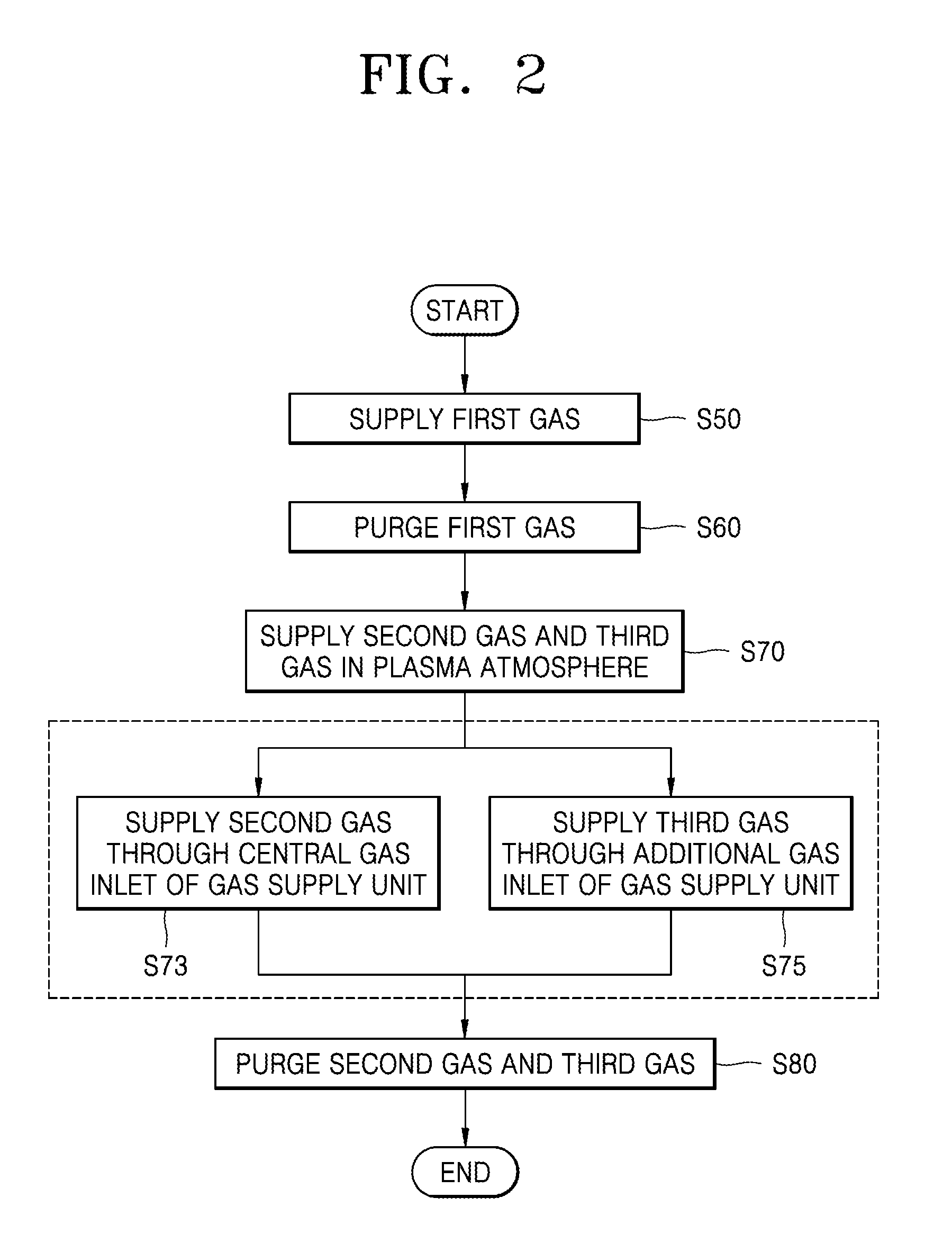
[0028] FIG. 2 is a flowchart of a substrate processing method according to other embodiments;
[0029] FIGS. 3 to 6 are cross-sectional views of a gas supply unit used in a substrate processing method according to embodiments and a substrate processing device including the gas supply unit;
[0030] FIG. 7 is a graph showing a degree of damage to a lower spin-on hardmask (SOH) film caused by a plasma radical when a silicon oxide (SiO.sub.2) film is deposited on an SOH film on a substrate;
[0031] FIG. 8 is a graph showing a degree of SOH loss in each region of a substrate when an SiO.sub.2 film is deposited on an SOH structure on the substrate under a plasma condition of 27 MHz and 600 watts;
[0032] FIG. 9 is a graph showing a change of SOH loss uniformity on a substrate when N.sub.2 gas is supplied instead of nitrous oxide (N.sub.2O), according to another embodiment; and
[0033] FIG. 10 is a graph schematically showing a substrate processing device according to other embodiments.
DETAILED DESCRIPTION
[0034] Reference will now be made in detail to embodiments, examples of which are illustrated in the accompanying drawings, wherein like reference numerals refer to like elements throughout. In this regard, the present embodiments may have different forms and should not be construed as being limited to the descriptions set forth herein. Accordingly, the embodiments are merely described below, by referring to the figures, to explain aspects of the present description. As used herein, the term "and/or" includes any and all combinations of one or more of the associated listed items. Expressions such as "at least one of," when preceding a list of elements, modify the entire list of elements and do not modify the individual elements of the list.
[0035] The terminology used herein is for the purpose of describing particular embodiments and is not intended to limit the present disclosure. As used herein, the singular forms "a", "an", and "the" are intended to include the plural forms as well, unless the context clearly indicates otherwise. It will be further understood that the terms "includes", "comprises" and/or "including", "comprising" used herein specify the presence of stated features, integers, steps, operations, members, components, and/or groups thereof, but do not preclude the presence or addition of one or more other features, integers, steps, operations, members, components, and/or groups thereof. As used herein, the term "and/or" includes any and all combinations of one or more of the associated listed items.
[0036] It will be understood that, although the terms first, second, etc. may be used herein to describe various members, components, regions, layers, and/or sections, these members, components, regions, layers, and/or sections should not be limited by these terms. These terms do not denote any order, quantity, or importance, but rather are only used to distinguish one component, region, layer, and/or section from another component, region, layer, and/or section. Thus, a first member, component, region, layer, or section discussed below could be termed a second member, component, region, layer, or section without departing from the teachings of embodiments.
[0037] In the present disclosure, "gas" may include evaporated solids and/or liquids and may include a single gas or a mixture of gases. In the present disclosure, the process gas introduced into a reaction chamber through a gas supply unit may include a precursor gas and an additive gas. The precursor gas and the additive gas may typically be introduced as a mixed gas or may be separately introduced into a reaction space. The precursor gas may be introduced together with a carrier gas such as an inert gas. The additive gas may include a dilution gas such as a reactant gas and an inert gas. The reactant gas and the dilution gas may be mixedly or separately introduced into the reaction space. The precursor may include two or more precursors, and the reactant gas may include two or more reactant gases. The precursor may be a gas that is chemisorbed onto a substrate and typically contains metalloid or metal elements constituting a main structure of a matrix of a dielectric film, and the reactant gas for deposition may be a gas that is reactive with the precursor chemisorbed onto the substrate when excited to fix an atomic layer or a monolayer on the substrate. The term "chemisorption" may refer to chemical saturation adsorption. A gas other than the process gas, that is, a gas introduced without passing through the gas supply unit, may be used to seal the reaction space, and it may include a seal gas such as an inert gas. In some embodiments, the term "film" may refer to a layer that extends continuously in a direction perpendicular to a thickness direction without substantially having pinholes to cover an entire target or a relevant surface, or may refer to a layer that simply covers a target or a relevant surface. In some embodiments, the term "layer" may refer to a structure, or a synonym of a film, or a non-film structure having any thickness formed on a surface. The film or layer may include a discrete single film or layer or multiple films or layers having some characteristics, and the boundary between adjacent films or layers may be clear or unclear and may be set based on physical, chemical, and/or some other characteristics, formation processes or sequences, and/or functions or purposes of the adjacent films or layers.
[0038] In the present disclosure, the expression "same material" should be interpreted as meaning that main components (constituents) are the same. For example, when a first layer and a second layers are both silicon nitride layers and are formed of the same material, the first layer may be selected from the group consisting of Si.sub.2N, SiN, Si.sub.3N.sub.4, and Si.sub.2N.sub.3 and the second layer may also be selected from the above group but a particular film quality thereof may be different from that of the first layer.
[0039] Additionally, in the present disclosure, according as an operable range may be determined based on a regular job, any two variables may constitute an operable range of the variable and any indicated range may include or exclude end points. Additionally, the values of any indicated variables may refer to exact values or approximate values (regardless of whether they are indicated as "about"), may include equivalents, and may refer to an average value, a median value, a representative value, a majority value, or the like.
[0040] In the present disclosure where conditions and/or structures are not specified, those of ordinary skill in the art may easily provide these conditions and/or structures as a matter of customary experiment in the light of the present disclosure. In all described embodiments, any component used in an embodiment may be replaced with any equivalent component thereof, including those explicitly, necessarily, or essentially described herein, for intended purposes, and in addition, the present disclosure may be similarly applied to devices and methods.
[0041] Hereinafter, embodiments of the present disclosure will be described with reference to the accompanying drawings. In the drawings, variations from the illustrated shapes may be expected as a result of, for example, manufacturing techniques and/or tolerances. Thus, the embodiments of the present disclosure should not be construed as being limited to the particular shapes of regions illustrated herein but may include deviations in shapes that result, for example, from manufacturing processes.
[0042] FIG. 1 is a flowchart of a substrate processing method according to embodiments of the present invention.
[0043] Referring to FIG. 1, in operation S10, a first material is supplied to a substrate on which a pattern structure is formed. The first material may be, for example, a source material and may include a material that is reactive with a second material to be supplied later. The first material may be a gas, a liquid, or a material in a state between a gas and a liquid. The first material may be supplied to the substrate on which the pattern structure is formed. Thus, the first material may be applied on top and bottom surfaces of the pattern structure and on a side connecting the top and bottom surfaces.
[0044] Thereafter, in operation S20, the second material is supplied to the substrate. The second material may be, in an embodiment, a reactant, and the pattern structure may include a material that is reactive with the reactant. In an embodiment, the pattern structure may include a photoresist. The second material may be a gas, and may be a liquid in alternative embodiment, or may be a material in a state between a gas and a liquid. The second material may be supplied in a plasma atmosphere. The second material may also be supplied at least near the center of the substrate through a supply unit (e.g., a gas supply unit). In operation S23, according to an embodiment, the second material may be supplied to the center of the substrate through a central gas inlet of the supply unit. In addition, the second material may be supplied to a portion other than the center of the substrate through another inlet of the supply unit.
[0045] In operation S20, during the supply of the second material, a blocking material other than the second material may also be supplied to the substrate. The blocking material may function to prevent a phenomenon wherein reactants are concentrated near an edge of the substrate (and thus, an edge of the pattern structure on the substrate is more damaged). The blocking material may include a material different from the first material and the second material.
[0046] In an embodiment, the blocking material may have greater ionization energy than ionization energy of the first material and ionization energy of the second material. In another embodiment, the blocking material may have ionization energy greater than that of an inert gas. The generation of a radical near the edge of the pattern structure on the substrate may be suppressed through the supply of the blocking material having such high ionization energy. Thus, damage to the pattern structure that is reactive with radical may be prevented.
[0047] As described above, the blocking material is a material that is supplied to block the concentration (and hence a radical formation) of reactants near the edge of the substrate. To this end, in operation S25, in an embodiment, the blocking material may be supplied through an additional gas inlet which is spaced apart from a central gas inlet of the supply unit. The additional gas inlet may be located between the central gas inlet of the supply unit and an edge of the supply unit. The blocking material may increase a flow at the edge of the substrate. Therefore, a radical density of the reactants near the edge of the substrate may be relatively reduced. In addition, a shielding effect on the radical density of the reactants near the center of the substrate may be occurred by supplying the blocking material to the edge of the substrate. Thus, the radical density of the reactants near the center of the substrate may be increased.
[0048] FIG. 2 is a flowchart of a substrate processing method according to other embodiments. The substrate processing method according to the other embodiments may be a variation of the substrate processing method according to the above-described embodiments. Hereinafter, repeated descriptions of the embodiments will not be given herein.
[0049] Referring to FIG. 2, in operation S50, a first gas is supplied to a substrate on which a pattern structure is formed. In an embodiment, the pattern structure may include a material that is reactive with oxygen, and a portion of the pattern structure may be removed by a reaction. In another embodiment, the pattern structure may include a material that is reactive with a material other than oxygen (e.g., nitrogen). In an embodiment, the pattern structure may include a spin-on hardmask (SOH).
[0050] The first gas may be a source gas as described above, and the first gas may be adsorbed on the substrate when the first gas is supplied to a reaction space. Thereafter, in operation S60, the first gas is purged. The first gas may include components of a thin film to be formed on the substrate. In an embodiment, when a silicon oxide film is to be formed on the substrate, the first gas may be a silicon-containing gas.
[0051] After the first gas is purged, in operation S70, a second gas and a third gas are supplied. The second gas and the third gas may be supplied in a plasma atmosphere. A substrate temperature during the process may be less than or equal to 100.degree. C. and, in a more specific example, less than or equal to 50.degree. C. A frequency of the plasma may be, for example, 27 MHz, and power of the plasma may be 600 W. However, it should be noted that the present disclosure is not limited to the above-described parameters and may be adjusted with various parameters.
[0052] The second gas may be a gas that is reactive with the first gas. On the other hand, the third gas may be a gas that is not reactive with the first gas. The first gas adsorbed on the substrate reacts with the second gas as the second gas is supplied, so that a thin film may be formed on the pattern structure. Since the first gas adsorbed on the substrate does not react with the third gas, the thin film formed on the pattern structure may not include components of the third gas.
[0053] The third gas may be a gas other than the first gas and the second gas. In order to prevent the thin film from containing the components of the third gas, the third gas may be selected as a material having high ionization energy. In an embodiment, the third gas may have ionization energy greater than that of the first gas and/or that of the second gas. In another embodiment, the third gas may have ionization energy greater than that of an inert gas. Accordingly, during the thin film forming process, the second gas may be ionized in a plasma atmosphere, while the third gas may not be ionized.
[0054] In an embodiment, when the first gas is a silicon-containing gas and the thin film to be formed is a silicon oxide film, the second gas may be an oxygen-containing gas and the third gas may be a nitrogen-containing gas. In an embodiment, the third gas may include at least one of a nitrous oxide (N.sub.2O) gas and an N.sub.2 gas.
[0055] In this case, during the formation of the silicon oxide film, the silicon-containing gas adsorbed on the pattern structure of the substrate may react with the oxygen-containing gas and not with the nitrogen-containing gas. This may be because the nitrogen-containing gas has ionization energy greater than that of the silicon-containing gas and that of the oxygen-containing gas. That is, only the oxygen-containing gas is ionized in a plasma atmosphere to react with the silicon-containing gas adsorbed on the substrate to form a silicon oxide film, and a silicon nitride film and/or a silicon oxynitride film may not be formed.
[0056] In an embodiment, when the second gas is an oxygen gas and the third gas is an N.sub.2O gas, a ratio of a flow of the oxygen gas to the N.sub.2O gas may be from 1:0.625 to 1:1.25. In an embodiment, when the flow of the oxygen gas is 160 sccm, a ratio of a flow of the N.sub.2O gas may be 100 sccm to 200 sccm. In another example, when the second gas is an oxygen gas and the third gas is an N.sub.2 gas, a ratio of the flow of the oxygen gas to the flow of the N.sub.2 gas may be from 1:0.625 to 1:1.25. In an embodiment, when the flow of the oxygen gas is 160 sccm, the flow of the N.sub.2 gas may be 100 sccm to 200 sccm. However, it should be noted that the present disclosure is not limited to the above-described parameters and may be adjusted with various parameters.
[0057] Although the above-described embodiments have been described on the basis of a process for forming a silicon oxide film, it is noted that the present disclosure is not limited thereto. The present disclosure may be a process for forming any oxide film, in which case the second gas may include an oxygen component and the third gas may include a nitrogen component. In another embodiment, the present disclosure may include a process for forming any nitride film.
[0058] In another embodiment, a temperature parameter in a plasma atmosphere may be a limiting factor for reactivity of the third gas. For example, the plasma atmosphere may be set to a first temperature, where the first gas (i.e., the first gas adsorbed on the pattern structure) reacts with the second gas at the first temperature, while the first gas may not react with the third gas at the first temperature. The first temperature may be, for example, 100.degree. C. or less.
[0059] In an embodiment, an oxygen gas supplied in a plasma atmosphere at a temperature of 100.degree. C. or less may react with the silicon-containing gas adsorbed on the pattern structure of the substrate to form a silicon oxide film. An N.sub.2 gas and/or an N.sub.2O gas supplied in the plasma atmosphere at a temperature of 100.degree. C. or less may not react with the silicon-containing gas adsorbed on the pattern structure of the substrate.
[0060] During the thin film forming process, in operation S73, the second gas may be supplied through at least a central gas inlet of a gas supply unit. On the other hand, in operation S75, the third gas may be supplied through an additional gas inlet that is spaced apart from the central gas inlet of the gas supply unit. As the third gas is supplied through the additional gas inlet, a flow at an edge of the substrate is increased, and thus a radical density of reactants near a center of the substrate may be increased. This may result in increased damage to the center of the substrate.
[0061] In more detail, when the second gas that is reactive with the pattern structure is supplied in the plasma atmosphere, the pattern structure may be removed or damaged as a radical of the second gas reacts with the pattern structure. Damage to such the pattern structure may be influenced by a position where the second gas is supplied, but may also be affected by a position where the third gas not involved in the reaction is supplied. In particular, when the third gas is supplied through the additional gas inlet, the generation of a radical that can react with the pattern structure at the edge may be suppressed, and thus damage to the pattern structure located at the edge of the substrate may be reduced.
[0062] For example, if the first gas is a silicon-containing gas, the second gas is an oxygen-containing gas, and the third gas is a nitrogen-containing gas, the oxygen-containing gas may be supplied at least through the central gas inlet. The nitrogen-containing gas may be supplied through the additional gas inlet that is spaced apart from the central gas inlet of the gas supply unit.
[0063] In this case, the nitrogen-containing gas may be supplied through the additional gas inlet to increase the flow at the edge of the substrate. Due to the increased flow at the edge of the substrate, density of the radical that is reactive with the pattern structure at the edge of the substrate may be reduced. Meanwhile, due to the increased flow at the edge of the substrate, density of the radical that is reactive with the pattern structure near the center of the substrate may be increased. As a result, the damage to the pattern structure at the edge of the substrate is reduced, and the damage to the pattern structure near the center of the substrate may be increased, and as a result, the both may become uniform.
[0064] In another embodiment, the oxygen-containing gas may be supplied through the additional gas inlet as well as the central gas inlet. That is, in order to control deviation of the damage to the pattern structure near the center of the substrate and the damage to the pattern structure near the edge of the substrate, through the additional gas inlet, the second gas (e.g., an oxygen-containing gas) that is reactive with the pattern structure and/or the third gas (e.g., a nitrogen-containing gas) that is not reactive with the pattern structure may be supplied.
[0065] The second gas and the third gas are supplied to form a thin film on the pattern structure, and in operation S80, the second gas and the third gas are purged. This completes one cycle for forming a thin film on the pattern structure, and the cycle may be repeated a predetermined number of times. By repeating the cycle, a thickness of the thin film formed on the pattern structure may be increased.
[0066] The thin film formed on the pattern structure may be used for a double patterning process or a quadruple patterning process. That is, in a later process, the pattern structure is removed, and the thin film formed on a side wall of the pattern structure serves as a mask, so that the substrate may be patterned.
[0067] As described in the above embodiments, the supply of a purge gas may be performed intermittently in a process of switching a gas. For example, a purge gas for purging the first gas may be intermittently supplied between the supply operation of the first gas and the supply operations of the second and third gases. A purge gas for purging the second and third gases may also be supplied between the supply operations of the second and third gases and the supply operation of the first gas in the next cycle.
[0068] In another embodiment, the supply of the purge gas may be performed continuously throughout a thin film forming process. For example, the purge gas for purging the first gas may be continuously supplied during the process. In this case, the purging of the first gas may be performed by not supplying another gas for a predetermined period from the supply operation of the first gas to the supply operations of the second and third gases. The purging of the second and third gases may be performed by not supplying another gas for a predetermined period from the supply operation of the second and third gases to the supply operation of the first gas in the next cycle.
[0069] Like the purge gas, the supply of the third gas may also be performed intermittently. For example, the third gas may be supplied between the supply operation of the second gas and the supply operation of the first gas in the next cycle. Also, the supply of the third gas may be performed continuously. In other words, the third gas may be continuously supplied throughout the thin film forming process.
[0070] FIG. 3 shows a gas supply unit used in a substrate processing method according to embodiments and a substrate processing device including the gas supply unit.
[0071] Referring to FIG. 3, the substrate processing device may include a partition wall 110, a gas supply unit 120, an RF load 130, and an exhaust path 140. Although a deposition device of a semiconductor or a display substrate is described herein as the substrate processing device, it is to be understood that the present disclosure is not limited thereto. The substrate processing device may be any device necessary for performing deposition of a material for forming a thin film, and may refer to a device in which a raw material for etching or polishing the material is uniformly supplied. Hereinafter, for convenience of description, it is assumed that the substrate processing device is a semiconductor deposition device.
[0072] The partition wall 110 may be a component of a reactor. In other words, a reaction space for treatment (e.g., deposition, etching, polishing) of a substrate may be formed by the partition wall 110. For example, the partition wall 110 may include a sidewall and/or upper wall of the reactor. The upper wall of the reactor in the partition wall 110 may provide a gas supply channel 150 through which a source gas, a purge gas, and/or a reaction gas may be supplied.
[0073] The gas supply unit 120 may be connected to the gas supply channel 150. The gas supply unit 120 may be fixed to the reactor. For example, the gas supply unit 120 may be fixed to the partition wall 110 via a fixing member (not shown). The gas supply unit 120 may be configured to supply a gas to an object to be processed in a reaction space 160. For example, the gas supply unit 120 may be a showerhead assembly.
[0074] A gas flow channel 170 communicating with the gas supply channel 150 may be formed in the gas supply unit 120. The gas flow channel 170 may be formed between a gas channel 125 (upper portion) of the gas supply unit 120 and a gas supply plate 127 (lower portion) of the gas supply unit 120. Although the gas channel 125 and the gas supply plate 127 are shown as separate structures in the drawings, the gas channel 125 and the gas supply plate 127 may be formed in an integrated structure.
[0075] The gas channel 125 may provide a central gas inlet connected to the gas supply channel 150. The central gas inlet may be connected to the gas flow channel 170 so that the gas flow channel 170 may be connected to the gas supply channel 150 through the central gas inlet.
[0076] As described above, the gas supply channel 150 may be formed in the partition wall 110. In addition to the gas supply channel 150, a first through hole 180 may be formed to penetrate at least a portion of the partition wall 110. For example, the first through hole 180 may be formed to penetrate the upper wall of the reactor in the partition wall 110. In a preferred embodiment, a diameter of the first through hole 180 may be less than that of the gas supply channel 150.
[0077] A second through hole 185 may be formed to penetrate at least a portion of the gas supply unit 120. For example, the second through hole 185 may be formed to connect with the gas flow channel 170 through the gas channel 125. Thus, the first through hole 180 may communicate with the gas flow channel 170 through the second through hole 185.
[0078] The second through hole 185 may be between the center and the edge of the gas flow channel 170. In particular, the second through hole 185 may be spaced apart from the edge of the gas flow channel 170. Through a positional structure of the second through hole 185, thin film deposition may be controlled at a specific portion of the substrate (that is, at a portion corresponding to the portion where the second through hole 185 is arranged).
[0079] In an embodiment, a gas supplied through the second through hole 185 may affect the degree of damage to the pattern structure at a lower portion, e.g. sub-layer such as spin-on-hardmask or SOH, of a thin film deposited between the center and the edge of the substrate. When the gas is a blocking gas having high ionization energy, the degree of damage to the pattern structure between the center and the edge of the substrate may be reduced.
[0080] The showerhead structure generally adopts a structure in which a reactive gas is supplied through the center portion and exhausted through the edge. Such a structure may cause a problem that damage to the pattern structure at the edge of the substrate and damage to the pattern structure at the center of the substrate become uneven. However, according to the present disclosure, a separate gas supply path may be added, through which a blocking gas may be supplied between a central portion and an edge of the reaction space. The supplied blocking gas may induce a blocking effect that limits radical generation around the reaction space and consequently damage to the pattern structure formed near the substrate may be reduced. Thus, the problem of deviation of the damage to the pattern structure occurring between the center and the edge of the substrate may be improved.
[0081] In another embodiment, a plurality of second through holes 185 may be formed along a circumference spaced apart from the center of the central gas inlet by a predetermined distance. In another alternative embodiment, the second through holes 185 may be continuously arranged along a circumference spaced apart from the center of the central gas inlet by a predetermined distance. In this case, the gas channel 125 may include a plurality of components separated by the second through hole 185.
[0082] The second through hole 185 may be formed to penetrate the gas channel 125 in a direction perpendicular or inclined relative to the gas supply plate 127 (or relative to the gas flow channel 170). For example, the second through hole 185 may be formed so as to penetrate the gas channel 125 at an angle of 15 to 45 degrees toward the center of the gas supply plate 127 with respect to an extending direction (that is, a horizontal direction) of the gas supply plate 127. In other words, by adjusting an penetration angle of the second through hole 185 penetrating the gas channel 125, uniformity of damage by a plasma to the pattern structure on the substrate and under the thin film may be controlled.
[0083] In an embodiment, the second through hole 185 may be formed so as to penetrate the gas channel 125 at an angle of 30 degrees with respect to the extending direction (that is, the horizontal direction) of the gas supply plate 127. In this case, the second through hole 185 may be arranged or formed along a first circumference having a first diameter on a first surface (e.g., an upper surface) of the gas channel 125, or may be arranged or formed along a second circumference having a second diameter on a second surface (e.g., a lower surface) of the gas channel 125, wherein the first diameter and the second diameter may be different from each other.
[0084] As such, the uniformity of damage to the pattern structure may be more precisely controlled by adjusting the number, shape, and arrangement position of the second through holes 185 and the kind and flow of gas supplied to the second through holes 185. As a result, a thin film of a desired shape and quality may be deposited.
[0085] In another embodiment, a buffer space 190 may be further formed between the first through hole 180 and the second through hole 185. The buffer space 190 may temporarily hold a gas so that the gas supplied through the first through hole 180 may be uniformly supplied to the second through hole 185. A diameter and width of the buffer space 190 may be greater than those of the first through hole 180 and may also be greater than those of the second through hole 185. In addition, the buffer space 190 may be continuously formed along a circumference spaced apart from the center of the gas supply channel 150 by a predetermined distance.
[0086] The substrate processing device may further include a gas supply channel 150, a first gas supply unit (not shown) connected to the gas supply channel 150 and a second gas supply unit (not shown) connected to the first through hole 180. The substrate processing device may further include a controller (not shown) configured to control the first gas supply unit and the second gas supply unit. In an embodiment, the controller may be further configured to independently control the first gas supply unit and the second gas supply unit. In an embodiment, the first gas supply unit may be configured to supply a source gas and/or a reactive gas, and the second gas supply unit may be configured to supply a blocking gas.
[0087] The substrate processing device may further include the RF load 130. The RF load 130 may be connected to the gas supply unit 120 through at least a portion of the partition wall 110. The RF load 130 may be connected to an external plasma supply unit (not shown). Although two RF loads 130 are shown in the drawing, the present disclosure is not limited thereto, and at least one or more RF loads 130 may be installed to improve uniformity of plasma power supplied to the reaction space 160.
[0088] The substrate processing device may further include a susceptor 200 configured to contact a lower surface of the partition wall 110. The susceptor 200 may be supported by a susceptor support 210, and the susceptor support 210 may move up and down and rotate. The susceptor 200 may be separated from the partition wall 110 or contact the partition wall 110 by the upward and downward movement of the susceptor support 210 so that the reaction space 160 may be opened or closed.
[0089] The substrate processing device may further include an exhaust unit (not shown). In the reaction space 160, a residual gas remaining after a chemical reaction with the substrate may be exhausted to the outside through the exhaust path 140 by the exhaust unit.
[0090] FIG. 4 schematically shows a gas supply unit and a substrate processing device including the gas supply unit according to other embodiments of the present disclosure. The gas supply unit and the substrate processing device according to the embodiments may be a variation of the substrate processing device according to the above-described embodiments. Hereinafter, repeated descriptions of the example embodiments will not be given herein.
[0091] Referring to FIG. 4, the substrate processing device may include the partition wall 110, the gas supply unit 120 which is substantially horizontally arranged in the partition wall 110, and the susceptor 200 which is arranged substantially opposite the gas supply unit 120 in the partition wall 110.
[0092] The exhaust path 140 provided in the partition wall 110 and connected by a vacuum pump may be used to evacuate a residual gas in the reaction space 160 in the partition wall 110.
[0093] The gas supply unit 120 may be a showerhead, and a base of the showerhead may include a plurality of holes 220 formed to eject a raw material gas. The showerhead may be connected to a raw material gas supply tank through the gas supply channel 150. A high frequency (RF) power may be electrically connected to a showerhead functioning as one electrode.
[0094] The susceptor 200 is supported by a support and may function as the other electrode. A substrate to be processed such as a semiconductor substrate may be loaded on a surface of the susceptor 200, and the substrate to be processed may be fixed by vacuum adsorption or the like.
[0095] Also, as described above, the second through hole 185 may be formed to penetrate at least a portion of an upper portion of the showerhead. Thus, the first through hole 180 may communicate with the gas flow channel 170 of the showerhead through the second through hole 185.
[0096] FIG. 5 schematically shows a gas supply unit and a substrate processing device including the gas supply unit according to other embodiments of the present disclosure. The gas supply unit and the substrate processing device according to the embodiments may be a variation of the substrate processing device according to the above-described embodiments. Hereinafter, repeated descriptions of the example embodiments will not be given herein.
[0097] Referring to FIG. 5, a first lid 240 including the partition wall 110 and a second lid 250 may form the reaction space 160 together with the susceptor 200. In more detail, a lower portion of the reaction space 160 may be formed by the susceptor 200, an upper portion of the reaction space 160 may be formed by the first lid 240, and both sides of the reaction space 160 may be formed by the second lid 250.
[0098] When the substrate processing device is a deposition device, the first lid 240 may include a showerhead. The second lid 250 may include a reaction sidewall W and an exhaust path 140.
[0099] An exhaust structure of the substrate processing device may be configured with a downstream exhaust structure, wherein the downstream exhaust structure may be implemented by the second lid 250. In this case, a gas used for deposition may be injected into a substrate to be processed through the showerhead of the first lid 240 and then exhausted downstream through the exhaust path 140 of the second lid 250.
[0100] Further, as described above, the second through hole 185 may be formed to penetrate at least a portion of an upper portion of the gas supply unit 125. Thus, the first through hole 180 may communicate with the gas flow channel 170 of the showerhead through the second through hole 185.
[0101] FIG. 6 schematically shows a gas supply unit and a substrate processing device including the gas supply unit according to other embodiments of the present disclosure. The gas supply unit and the substrate processing device according to the embodiments may be a variation of the substrate processing device according to the above-described embodiments. Hereinafter, repeated descriptions of the example embodiments will not be given herein.
[0102] As described above, the present disclosure discloses a method of controlling characteristics of each portion of a thin film deposited on a substrate. According to the present disclosure, thin film deposition using plasma is performed on a substrate in a reactor provided with a gas supply device for supplying a gas to the substrate. In more detail, the gas supply device is a showerhead, and the thin film deposition using plasma may be one of plasma atomic layer deposition (PEALD), plasma enhanced chemical vapor deposition (PECVD), pulsed PECVD, and cyclic pulsed PECVD, or a suitable combination of the methods, or may be a suitable variant of the methods.
[0103] Referring to FIG. 6, a reaction space 13 is formed by a reactor 1 through a face contact between a reactor wall 2 and a susceptor 3. A gas is supplied to the reaction space 13 through a first gas inlet 4 located at the center of the reactor 1 and a second gas supply port 8 and second gas inlets 5, 6, and 7 located around the reactor 1, and holes (not shown) of a showerhead 11 located therebelow.
[0104] The gas supplied to the reaction space 13 reacts with a surface of a substrate (not shown) loaded on the susceptor 3 and thereafter is exhausted through an exhaust channel 14, an exhaust hole 15, an exhaust path 16, and an exhaust port. The second gas inlets 5, 6, and 7 may be connected to a gas flow channel 12 through the reactor wall 2, a back plate 9, and a gas channel 10. For example, the second gas inlet 7 through the gas channel 10 may be formed at various angles with respect to a substrate surface. Whereby a flow of gas supplied to a specific portion on the substrate may be controlled and characteristics of a thin film deposited on a specific portion on the substrate may be controlled.
[0105] The second gas inlet 5 through the reactor wall may penetrate one surface of the reactor. The second gas inlets 6 and 7 may be arranged annularly with respect to the center of the reactor, whereby a second gas may be uniformly supplied to a peripheral portion of the substrate.
[0106] FIG. 7 shows a degree of damage to a sublayer SOH film caused by a plasma radical when an SiO.sub.2 film is deposited on an SOH (one type of a photo-resist) film on a substrate by the PEALD method in the reactor of FIG. 6. The degree of damage is measured by wet-etching the deposited SiO.sub.2 film.
[0107] Referring to FIG. 7, a horizontal axis represents angular positions in both directions from the center of a substrate with a diameter of 300 mm, and a vertical axis represents the degree of loss of the sublayer SOH film depending on a flow of oxygen or an inert gas (e.g., argon (Ar)) supplied through the second gas supply path of FIG. 6 when the SiO.sub.2 film is deposited by a plasma ALD method. In the reactor of FIG. 6, 50 sccm of oxygen, 250 sccm of oxygen, 600 sccm of Ar, and 1000 accm of Ar were supplied through the second gas inlet, but a form and degree of the SOH film loss over the entire substrate were similar regardless of a gas type and flow.
[0108] In more detail, referring to FIG. 7, SOH loss uniformity of the sublayer SOH film is not uniform over the entire substrate, and the SOH film loss at the edge of the substrate is large. This means that a plasma radical density throughout a reaction space during plasma processing is not constant and a radical density at the edge of the substrate is particularly high. Therefore, in the present disclosure, a method of increasing the SOH loss uniformity as a whole by controlling the radical density at the edge of the substrate is disclosed.
[0109] In order to control or lower a radical density in a peripheral portion of the substrate (a region between the central portion of the substrate and the edge of the substrate), a gas for suppressing radical generation is supplied in the present disclosure. According to an embodiment of the present disclosure, when the SiO.sub.2 film is deposited using plasma on the SOH film, a nitrogen-containing gas is supplied through the second gas inlet. In more detail, when a source gas, an oxygen reactive gas, and an Ar carrier gas or a purge gas are supplied through the first gas inlet, an N.sub.2 gas is supplied through the second gas inlet. The ionization energy of the N.sub.2 gas is 1,503 MJ/mol, ionization energy of the Ar gas is 1,520.6 KJ/mol, and ionization energy of an oxygen gas is 493.4 KJ/mol. Dissociation energy of an N.sub.2 gas is much larger than dissociation energy of other gases. Therefore, when N.sub.2 is supplied, plasma generation may be suppressed compared with a case where argon or oxygen is supplied. Besides the N.sub.2 gas, gas with greater ionization energy than ionization energy of the Ar carrier gas, the purge gas, or the oxygen reactive gas may be supplied through the second gas inlet.
[0110] As such, according to the present disclosure, the SOH loss in the peripheral portion may be prevented by suppressing radical generation in the peripheral portion of the substrate corresponding to the second gas inlet port as compared with the central portion of the substrate, and more uniform SOH loss uniformity may be achieved as a whole.
[0111] FIG. 8 is a graph showing a degree of SOH loss in each region of a substrate when an SiO.sub.2 film is deposited on an SOH structure on the substrate under a plasma condition of 27 MHz and 600 watts. The substrate has a diameter of 300 mm and the SOH loss is measured at each position at a distance of 150 mm on both sides of the center of the horizontal axis, that is, the center of the substrate. A vertical axis represents the degree of SOH loss measured in angstrom units.
[0112] Referring to FIG. 8, when an oxygen gas is supplied together with an Ar gas and the SOH loss is measured according to the amount of the nitrogen-containing gas (e.g., N.sub.2O) supplied to the peripheral portion of the substrate through the second gas inlet, the SOH loss at the peripheral portion of the substrate decreases as a flow of the nitrogen-containing increases. That is, when only the oxygen gas and the Ar gas are supplied, the SOH loss uniformity on the substrate is poor. However, when a ratio of the nitrogen-containing gas is increased instead of Ar, plasma generation at the peripheral portion of the substrate is suppressed, and hence damage to the SOH layer by a radical may be reduced. As a result, it can be seen that the SOH loss uniformity may be generally controlled and gradually improved. Further, referring to FIG. 8, as the supply amount of an N.sub.2O gas increases, the SOH loss at the edge of the substrate decreases but the SOH loss at the center increases rather. This can be understood that as an N.sub.2O gas supplied to the peripheral portion of the substrate surrounds an oxygen gas supplied to the center portion, an oxygen radical density in the central portion is relatively increased and the SOH loss is increased. Accordingly, it is shown that a radical density at the center of the substrate may be controlled by appropriately controlling a ratio of a flow of the nitrogen-containing gas supplied to the peripheral portion of the substrate, and the SOH loss uniformity or uniformity of sublayer deformation may be appropriately controlled.
[0113] FIG. 9 is a graph showing a change of SOH loss uniformity on a substrate when an N.sub.2 gas is supplied instead of N.sub.2O. Referring to FIG. 9, it can be seen that the SOH loss uniformity may be controlled according to a flow of an edge N.sub.2 gas EN when the N.sub.2 gas is supplied to the peripheral portion of the reaction space through the first gas inlet and the second gas inlet.
[0114] FIG. 10 is a graph schematically showing a substrate processing device according to other embodiments. The substrate processing method according to the other embodiments may be a variation of the substrate processing method according to the above-described embodiments. Hereinafter, repeated descriptions of the example embodiments will not be given herein.
[0115] Referring to FIG. 10, a Si source gas, an oxygen gas, and an Ar gas are supplied to a reaction space through a first gas inlet at the center of a reaction space, and N.sub.2 or N.sub.2O is supplied to a peripheral portion of the reaction space through a second gas inlet near the reaction space. The oxygen gas may be supplied through the first gas inlet in the form of a pulse as shown in FIG. 10, or may be continuously supplied. According to the present disclosure, a ratio of the N.sub.2 gas is relatively high in the peripheral portion of the substrate, and the degree of radical generation is relatively small as compared with those at the center and the edge of the substrate. Therefore, SOH loss at the peripheral portion may be reduced and the overall SOH loss uniformity may be improved (see FIGS. 8 and 9).
[0116] As such, according to the present disclosure, in a plasma deposition process, by supplying a gas having greater ionization energy than that of a reactive gas and a carrier gas to the peripheral portion between the center and the edge of the substrate, radical generation in the peripheral portion is suppressed relative to radical generation in the center and the edge, and sublayer loss uniformity of the entire substrate may be improved by controlling sublayer loss at the peripheral portion.
[0117] Shapes of each portion of accompanying drawings for a clear understanding of the present disclosure should be considered in descriptive sense, but may be modified into various shapes other than those shown.
[0118] It should be understood that the embodiments described herein should be considered in a descriptive sense only and not for purposes of limitation. Descriptions of features or aspects within each embodiment should typically be considered as available for other similar features or aspects in other embodiments.
[0119] While one or more embodiments have been described with reference to the figures, it will be understood by those of ordinary skill in the art that various changes in form and details may be made therein without departing from the spirit and scope of the disclosure as defined by the following claims.
* * * * *
D00000
D00001
D00002
D00003
D00004
D00005
D00006
D00007
XML
uspto.report is an independent third-party trademark research tool that is not affiliated, endorsed, or sponsored by the United States Patent and Trademark Office (USPTO) or any other governmental organization. The information provided by uspto.report is based on publicly available data at the time of writing and is intended for informational purposes only.
While we strive to provide accurate and up-to-date information, we do not guarantee the accuracy, completeness, reliability, or suitability of the information displayed on this site. The use of this site is at your own risk. Any reliance you place on such information is therefore strictly at your own risk.
All official trademark data, including owner information, should be verified by visiting the official USPTO website at www.uspto.gov. This site is not intended to replace professional legal advice and should not be used as a substitute for consulting with a legal professional who is knowledgeable about trademark law.