Electromagnetic Radiation Detector Based On Wafer Bonding
VON KAENEL; Hans
U.S. patent application number 16/430581 was filed with the patent office on 2019-09-19 for electromagnetic radiation detector based on wafer bonding. The applicant listed for this patent is G-RAY INDUSTRIES SA. Invention is credited to Hans VON KAENEL.
| Application Number | 20190288026 16/430581 |
| Document ID | / |
| Family ID | 61911637 |
| Filed Date | 2019-09-19 |
View All Diagrams
| United States Patent Application | 20190288026 |
| Kind Code | A1 |
| VON KAENEL; Hans | September 19, 2019 |
ELECTROMAGNETIC RADIATION DETECTOR BASED ON WAFER BONDING
Abstract
Monolithic pixel detectors, systems and methods for the detection and imaging of electromagnetic radiation with high spectral and spatial resolution comprise a Si wafer with a CMOS processed pixel readout bonded to an absorber wafer in wafer bonds comprising conducting bonds between doped, highly conducting charge collectors in the readout and highly conducting regions in the absorber wafer and poorly conducting bonds between regions of high resistivity.
| Inventors: | VON KAENEL; Hans; (Wallisellen, CH) | ||||||||||
| Applicant: |
|
||||||||||
|---|---|---|---|---|---|---|---|---|---|---|---|
| Family ID: | 61911637 | ||||||||||
| Appl. No.: | 16/430581 | ||||||||||
| Filed: | June 4, 2019 |
Related U.S. Patent Documents
| Application Number | Filing Date | Patent Number | ||
|---|---|---|---|---|
| PCT/IB2018/000166 | Mar 1, 2018 | |||
| 16430581 | ||||
| Current U.S. Class: | 1/1 |
| Current CPC Class: | H01L 27/14636 20130101; H01L 27/14659 20130101; H01L 31/1832 20130101; H01L 31/028 20130101; H01L 27/14696 20130101; H01L 27/1463 20130101; H01L 27/14634 20130101; H01L 31/1804 20130101; H01L 27/14649 20130101; H01L 2223/54493 20130101; H01L 27/14689 20130101; H04N 5/378 20130101; H01L 27/14661 20130101; H01L 31/02966 20130101; H01L 31/1892 20130101; G01N 23/046 20130101; H01L 27/1464 20130101; H01L 27/14658 20130101; H01L 27/1469 20130101; H01L 31/03046 20130101; H01L 27/14638 20130101; H01L 31/107 20130101; H01L 27/14694 20130101; H01L 27/14676 20130101; H01L 27/1465 20130101; H01L 23/544 20130101; H01L 2223/54426 20130101; H01L 31/1812 20130101; H01L 31/1844 20130101 |
| International Class: | H01L 27/146 20060101 H01L027/146; H01L 31/107 20060101 H01L031/107; H04N 5/378 20060101 H04N005/378; G01N 23/046 20060101 G01N023/046 |
Foreign Application Data
| Date | Code | Application Number |
|---|---|---|
| Mar 1, 2018 | IB | PCT/IB2018/000166 |
Claims
1. A monolithic CMOS integrated pixel detector for the detection of electromagnetic radiation configured for backside illumination, comprising a silicon readout wafer made from silicon of a first doping type, comprising CMOS pixel readout electronics processed in a thin silicon layer and including highly conducting doped regions of a second doping type acting as charge collectors spaced at a pixel size L, the charge collectors communicating with the readout electronics; said readout wafer being bonded by wafer bonds to an absorber wafer made from at least one single crystal semiconductor material, the absorber wafer further comprising highly conducting doped regions; the pixel detector further comprising the readout wafer bonded, in an aligned manner, to the absorber wafer; wherein said wafer bonds comprise highly conducting bonds between the readout wafer and the absorber wafer and poorly conducting bonds between the readout wafer and the absorber wafer, the poorly conducting bonds having a resistance exceeding that of the highly conducting bonds at least by a factor of 10.sup.2 thereby electrically isolating neighboring pixels so as to force charges generated in the absorber wafer to cross the conducting bonds and to be received by the charge collectors for processing by the pixel readout electronics when the detector is in operation.
2. The monolithic CMOS integrated pixel detector of claim 1, wherein the conducting bonds between the readout wafer and the absorber wafer are conducting covalent semiconductor bonds and wherein the poorly conducting bonds between the readout wafer and the absorber wafer are bonds between regions at least one of which is a highly resistive or insulating region or a p-n junction polarized in reverse direction when the detector is in operation, and wherein the poorly conducting bonds have a resistance exceeding that of the conducting covalent bonds at least by a factor selected from one of the group of ranges of factors consisting of 10.sup.2-10.sup.4, 10.sup.4-10.sup.6 and 10.sup.6-10.sup.8.
3. The monolithic CMOS integrated pixel detector of claim 1, wherein the thin silicon layer has a thickness selected from one of the group of thicknesses consisting of 10-30 .mu.m, 5-10 .mu.m and 3-5 .mu.m.
4. The monolithic CMOS integrated pixel detector of claim 1, wherein the highly conducting doped regions of the readout wafer and the highly conducting doped regions of the absorber wafer have a doping range selected from one of the group of doping ranges consisting of 1.times.10.sup.18-1.times.10.sup.19 cm.sup.-3, 1.times.10.sup.19-1.times.10.sup.20 cm.sup.-3 and 1.times.10.sup.20-5.times.10.sup.20, cm.sup.-3.
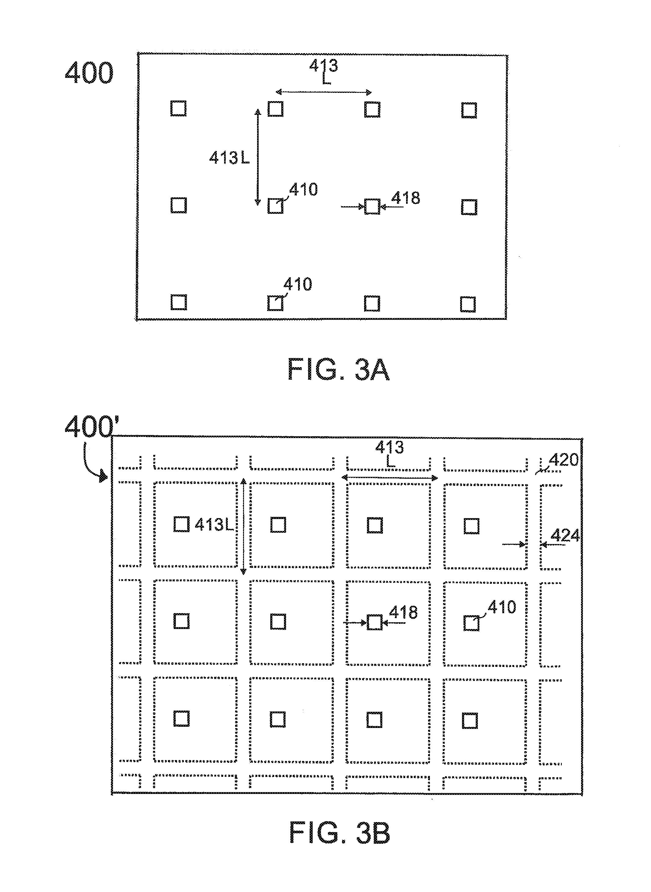
5. The monolithic CMOS integrated pixel detector of claim 1, further including wafer alignment features aligning the readout wafer with the absorber wafer selected from one of the group of features consisting of wafer notches, wafer flats and alignment marks.
6. The monolithic CMOS integrated pixel detector of claim 1 adapted for the detection of infrared radiation.
7. The monolithic CMOS integrated pixel detector of claim 6, wherein the pixel size L is in the range of 2-40 .mu.m.
8. The monolithic CMOS integrated pixel detector of claim 7, wherein the absorber wafer is pixelated in the form of absorber patches mutually isolated by insulating regions.
9. The monolithic CMOS integrated pixel detector of claim 8, wherein the absorber patches are spaced by the pixel size L of the detector pixels.
10. The monolithic CMOS integrated pixel detector of claim 8, wherein the absorber patches have a first width and the insulating regions have a second width, and wherein the sum of widths and is equal the pixel size L of the detector or a multiple thereof.
11. The monolithic CMOS integrated pixel detector of claim 7, wherein highly resistive regions in the silicon readout wafer provide electrical isolation between neighboring pixels.
12. The monolithic CMOS integrated pixel detector of claim 7, wherein the at least one single crystal semiconductor material of the absorber wafer is made of at least one of the group of materials consisting of Si, Ge, SiGe alloys, SiGeSn alloys, InAs, InGaAs alloys, InSb, the lead salts PbS, PbSe, PbTe and their alloys, and HgCdTe alloys.
13. The monolithic CMOS integrated pixel detector of claim 12, wherein the at least one single crystal semiconductor material of the absorber wafer is made from an epitaxial wafer comprising at least one epitaxial layer on a single crystal substrate.
14. The monolithic CMOS integrated pixel detector of claim 13, wherein the at least one epitaxial layer is a Ge, SiGe, SiGeSn, InGaAs, PbSeTe or HgCdTe alloy layer.
15. The monolithic CMOS integrated pixel detector of claim 12, wherein the absorber wafer comprises a charge multiplication layer.
16. The monolithic CMOS integrated pixel detector of claim 1, wherein the silicon readout wafer comprises a charge multiplication layer.
17. The monolithic CMOS integrated pixel detector of claim 1, wherein an at least one alignment feature of the readout wafer is superimposed on an at least one alignment feature of the absorber wafer with the rotational misalignment of the two wafers kept within about 0.1 to 0.2 degrees, and the lateral displacement within about 200-400 .mu.m.
18. The monolithic CMOS integrated pixel detector of claim 1, wherein an at least one alignment feature of the readout wafer is superimposed on an at least one alignment feature of the absorber wafer with the rotational misalignment of 200 mm wafers kept within about (2-5).times.10.sup.-4 degrees and the lateral misalignment within about 0.1-1 .mu.m.
19. The monolithic CMOS integrated pixel detector of claim 1, wherein the second doping type is of an opposite doping type to that of the first doping type.
20. The monolithic CMOS integrated pixel detector of claim 1, wherein the second doping type is of a similar doping type to that of the first doping type.
21. A method for forming a monolithic CMOS integrated pixel detector for the detection of electromagnetic radiation, the method comprising a) providing a pixel readout electronics by CMOS processing of a silicon readout wafer; b) forming highly conducting regions in the readout wafer spaced at a pixel size L acting as charge collectors and communicating with the pixel readout electronics; c) forming at least one alignment feature in the readout wafer; d) forming an absorber wafer from at least one single crystal semiconductor material; e) forming highly conducting doped regions in the absorber wafer; ff) forming at least one alignment feature in the absorber wafer; g) bonding a carrier wafer to the CMOS stack of the readout wafer after planarizing the CMOS stack; h) thinning and planarizing the readout wafer; i) superimposing the at least one alignment feature of the readout wafer and the absorber wafer; j) forming wafer bonds comprising highly conducting bonds and poorly conducting bonds between the readout wafer and the absorber wafer; wherein the poorly conducting bonds have a resistance exceeding that of the highly conducting bonds at least by at least 10.sup.2; and k) partially or completely removing the carrier wafer from the CMOS stack and opening bonding pads on the CMOS stack.
22. The method of claim 21, wherein the forming of the highly conducting wafer bonds comprises forming covalent conducting bonds and wherein the forming of poorly conducting bonds between the readout wafer and the absorber wafer comprises forming bonds between regions at least one of which is a highly resistive or insulating region or forming bonds between semiconductor regions of opposite doping which become poorly conducting when the p-n junction is polarized in reverse direction during detector operation.
23. The method of claim 22, wherein forming the absorber wafer comprises forming the absorber wafer in the form of absorber patches separated by insulating regions.
24. The method of claim 22, wherein the forming of the absorber wafer from the at least one single crystal semiconductor material comprises forming an absorber wafer adapted for infrared detection from at least one material selected from one of the group of materials consisting of Si, Ge, SiGe alloys, SiGeSn alloys, InAs, InGaAs alloys, InSb, PbS, PbSe, PbTe, PbSeTe alloys and HgCdTe alloys.
25. The method of claim 24, wherein forming the absorber wafer comprises forming at least one epitaxial layer on a single crystal substrate.
26. The method of claim 25, wherein forming the at least one epitaxial layer on a single crystal substrate comprises forming the epitaxial layer on one substrate selected from one of the group of substrates consisting of Si, Ge, GaAs, InSb, CdTe and CdZnTe.
27. The method of claim 26, wherein forming the absorber wafer with the at least one epitaxial layer on the single crystal substrate comprises steps of: a) providing a dielectric layer on the single crystal substrate; b) opening windows in the dielectric layer consisting of first windows of narrower width extending to the single crystal substrate and second windows of wider width with dielectric sidewalls of a first height; c) growing a first layer into first narrow windows and subsequently overgrowing the dielectric in the wider second windows to a second height by a selective epitaxy process; d) growing a second layer in the wider second windows to a third height, such that the sum of the second height and third height is below the first height of the dielectric sidewalls of said windows; e) growing a third layer in wider second windows with a faceted surface to a level above the dielectric sidewalls; f) planarizing the faceted surface to remove the facets so as to generate a planar, smooth and essentially particle-free surface of the absorber wafer with a surface roughness of 0.3-0.5 nm or 0.1-0.3 nm, suitable for low temperature wafer bonding to a thinned CMOS processed readout wafer.
28. The method of claim 26, wherein forming the absorber wafer with the at least one epitaxial layer on the single crystal substrate comprises the steps of: a) providing a patterned substrate for epitaxy in the form of pillars separated by trenches; b) epitaxially growing SiGe alloy crystals with gaps on top of the pillars; c) filling trenches and gaps between the SiGe crystals with insulating material; and d) providing a flat and smooth surface with an RMS roughness below 0.5 nm or preferably about 0.1-0.3 nm of the absorber wafer by planarizing the surface of the SiGe alloy crystals by CMP to make it suitable for wafer bonding with a thinned CMOS processed readout wafer.
29. The method of claim 27, wherein forming the at least one epitaxial layer comprises forming a charge multiplication layer.
30. The method of claim 28, wherein forming the at least one epitaxial layer comprises forming a charge multiplication layer.
31. The method of claim 23, wherein the CMOS processing of the readout wafer includes forming a charge multiplication layer.
32. The method of claim 25, wherein forming the monolithic CMOS integrated pixel detector includes removing the single crystal substrate.
33. The method of claim 23, wherein forming the monolithic CMOS integrated pixel detector further includes forming a metallic back contact.
34. A detector made according to the method of claim 21, the detector having single photon detection capability when operated in Geiger mode.
35. The detector of claim 34, wherein the absorber comprises an absorber region and an avalanche region made from a semiconductor with a larger bandgap than that of the absorber region, and wherein the avalanche region of the absorber communicates with the charge collectors of the readout wafer.
36. The detector of claim 34, wherein the readout wafer comprises a Si avalanche region communicating with the charge collectors, and wherein the absorber comprises at least one semiconductor with a lower bandgap than that of the avalanche region.
37. A device for non-destructive testing having the detector of claim 1, wherein the device includes: a) at least one switchable X-ray source with power supply b) at least one X-ray detector communicating with readout unit, c) one computerized control, data processing and display unit, one sample rotatable around at least one of the rotation axes, wherein the power supply of the at least one X-ray source and the readout unit of the at least one X-ray detector communicate with and are synchronized by the computerized control, data processing and display unit controlling also the sample rotation in order to generate, process and display computed tomography images.
38. A device for non-destructive testing having a plurality of the detectors of claim 1, wherein the device includes at least: a) one switchable X-ray source with power supply, b) one array of X-ray detectors communicating with readout units, c) one computerized control, data processing and display unit, and d) data communication and control lines, wherein the power supply of the at least one X-ray source and the readout units of the at least one array of X-ray detectors are interconnected by the communication and control lines and communicate with and are synchronized by the computerized control, data processing and display unit to generate, process and display computed tomography images.
39. A vehicle equipped for assisted or autonomous driving having detectors of claim 1, wherein the equipment of the vehicle includes at least: a) an array of spatially separated infrared detectors communicating with readout units, and b) data communications and power supply lines interconnecting all readout units and detectors to an on-board control and data processing center communicating with the data communications and power supply lines, wherein the array of spatially separated and interconnected infrared detectors permits real time distance measurements from static and moving objects through triangulation.
Description
CROSS REFERENCE TO RELATED APPLICATIONS
[0001] This application is a continuation in part of PCT application no. PCT/IB2018/000166, filed 1 Mar. 2018, of the same title, which claims priority to and benefit of U.S. Provisional Application No. 62/465,199 filed 1 Mar. 2017, which is incorporated herein by reference and relied upon.
FIELD OF THE INVENTION
[0002] The invention relates to pixel detectors made from monolithic, Complementary Metal Oxide Semiconductor (CMOS) integrated structures for the detection and imaging of electromagnetic radiation, and to methods for forming such structures.
BACKGROUND OF THE INVENTION
[0003] Digital imaging devices for electromagnetic radiation detection, also called pixel detectors, convert the energy of absorbed photons into electrical signals. For high-energy (i.e., typically much greater than 1 keV) electromagnetic radiation detection, current digital imaging devices can be classified into two broad classes, distinguished by the way in which impacting photons are converted into electrical signals. Taking X-ray photons as an example, in the first one of these classes, the conversion happens indirectly in the sense that X-ray photons are first down-converted in energy to visible photons in a scintillation layer. The visible photons are subsequently detected by an array of photodiodes, in which the optical generation of electron-hole pairs gives rise to electrical signals which are then further processed by a readout electronics and represented as an image on a computer screen. The two-stage conversion process of indirect X-ray imaging devices suffers from the drawback of limited conversion efficiency and spatial resolution because of losses and scattering occurring both during the conversion of X-rays into visible photons and in the detection of those. Typically about 25 electron-hole pairs are finally measured by the readout electronics per keV of incident X-ray energy.
[0004] In the second class of these pixel detectors semiconductor absorbers permit the direct conversion of X-rays into electron-hole pairs which can then be measured as an electrical signal by a readout electronics. In addition to superior sensitivity and higher spatial and temporal resolution compared to scintillator-based indirect conversion, such absorbers offer also spectral resolution, since the energy of an incident X-ray photon is proportional to the number of generated electron-hole pairs and thus measurable by a pulse height analysis. In silicon (Si), one needs on average 3.6 eV to create a single electron-hole pair (see for example R. C. Alig et al. in Phys. Rev. B 22, 5565 (1980); and R. C. Alig in Phys. Rev. B 27, 968 (1983), the entire disclosures of which are hereby incorporated by reference). On average this leads to 280 electron-hole pairs per keV of absorbed X-ray energy, from which it can be seen that the conversion efficiency exceeds that of a scintillator-photodiode combination by more than a factor of ten.
[0005] X-ray imaging detectors, or pixel sensors in general, employing direct conversion by means of semiconductor absorbers, can be implemented in different ways. One approach used in commercial flat panel fabrication is based on polycrystalline or amorphous materials directly deposited on the readout electronics made from thin film transistors. For example flat panel X-ray imaging detectors with amorphous selenium absorbers for medical applications are relatively inexpensive to make and offered in large sizes (see for example S. Kasap et al. in Sensors 11, 5112 (2011), the entire disclosure of which is hereby incorporated by reference). Materials in the form of single crystals offer, however, much better transport properties compared with their polycrystalline and amorphous counterparts. They therefore should provide improved detector performance. Single crystal absorbers are on the other hand incompatible with readout electronics made up of amorphous thin film transistors. They can in principle be epitaxially grown on CMOS processed readout wafers, but usually only at the expense of an intolerably high thermal budget, requiring special metallization schemes compatible with elevated process temperatures (see for example U.S. Pat. No. 8,237,126 to von Kanel, the entire disclosure of which is hereby incorporated by reference). Typically, with standard aluminium metallization, temperatures have to be kept below 450.degree. C.
[0006] Pixel detectors for visible and near infrared radiation detection are well known for example from mobile phones. In such detectors absorber and readout unit are both fabricated from a common silicon substrate. They are therefore true monolithic structures which do not require any bonding process in order to establish electrical connections between absorber and readout. Such monolithic detectors are also used for high-energy elementary particle detection.
[0007] On the other hand, pixel detectors consisting of a CMOS processed readout and an absorber made from a semiconductor other than silicon, require a low-temperature bonding process to establish electrical connections between every absorber pixel and the pixel electronics of the readout wafer. A low-temperature bonding process is required to be compatible with the CMOS processed readout electronics. Direct epitaxial growth of the absorber onto the readout electronics may be a possible exception, provided that the temperature can be kept sufficiently low. The most common bonding technique is bump bonding, as used for example by the Medipix collaboration (medipix.web.cern.ch) or by Dectris AG (dectris.ch). Bump bonding of detector areas beyond a few cm.sup.2 is not only a costly technique but also limits the pixel size typically to about 50 pin. The absorber can in principle consist of any semiconductor material suitable for energetic particle detection from which large single crystals can be grown, for example Si, Ge, GaAs and CdTe or CdZnTe alloys (see for example European Patent No. 0571135 to Collins et al., the entire disclosure of which is hereby incorporated by reference). The higher the order number Z of an absorber of given thickness, the more photons of a given energy it will absorb. Hence a 1 mm thick Si absorber will absorb more than 90% of incident photons up to an energy of about 15 keV, a Ge or GaAs absorber of the same thickness absorbs at least 90% photons with energies below about 45 keV, and finally an equally thick CdTe absorber manages more than 90% absorption up to photon energies of about 72 keV.
[0008] Bump bonding for example with In micro-bumps is also used for the fabrication of infrared focal plane arrays, where a pixel size of 15 .mu.m is in production and 10 .mu.m or even smaller appears feasible. Typically, these arrays are much smaller in area than the ones used for X-ray imaging, hardly ever exceeding about 1 cm.sup.2 (see for example P. Bensussan et al. in Proc. of SPIE, Vol. 7298, pp. 72982N-1-72982N-31 (2009), the entire disclosure of which is hereby incorporated by reference). For infrared imaging, additional absorber materials are in use, such as InGaAs alloys, InSb and HgCdTe alloys or also lead salts.
[0009] While for large X-ray detectors it is hard to push the pixel size to below about 50 .mu.m with ordinary bump bonding, there are other bonding technologies potentially offering higher detector resolution. One of them is for example known from the vertical integration of integrated circuits, so-called 3D-IC technology. Here, bump bonding is replaced by fusion bonding, made up of oxide-to-oxide fusion bonding along with metal-to-metal bonding of metallic pads surrounded by oxide. The resulting structures are indistinguishable from genuine monolithic configurations (see for example G. W. Deptuch et al. in IEEE Trans. Nucl. Sci. 57, 2178 (2010), the entire disclosure of which is hereby incorporated by reference). For this reason we shall in the following consider heterostructures made by direct wafer bonding as monolithic as if they were fabricated for example in the form of epitaxial wafer stacks.
[0010] In yet another bonding technique, an electrically conductive, covalent semiconductor bond is formed at low temperature between the absorber wafer and the readout wafer. Covalent semiconductor bonding essentially leads again to a monolithic structure (see for example U.S. Pat. No. 10,163,957 to von Kanel, the entire disclosure of which is hereby incorporated by reference). In contrast to the well-known hydrophobic and hydrophilic bonding techniques in which the surfaces are respectively hydrogen or oxide covered prior to the bonding, covalent semiconductor bonding requires the surfaces to be atomically clean, especially when silicon is one of the bonding partners. Covalent semiconductor bonding can therefore only be carried out in a high vacuum or even ultra-high vacuum tool. In an ideal situation, when two essentially perfectly flat semiconductor wafers to be covalently bonded are very accurately aligned, neither with any mutual twist nor tilt, the dangling bonds on the two surfaces form covalent bonds that are indistinguishable from the bonds formed during epitaxial growth once the two wafers are brought into contact. Evidently, in practice such an ideal situation never occurs, and finite surface roughness and misalignment always lead to a finite number of interfacial defects, even when the two wafers are made from the same semiconductor material. Depending on the CMOS process used the pixel size can vary in a wide range for example of about 100-200 .mu.m, 50-100 .mu.m, 20-50 .mu.m, or 5-20 .mu.m, or even 2-5 .mu.m.
[0011] In this bonding approach, charge carriers are generated by backside illumination, wherein the absorber wafer is bonded on the thinned Si substrate of the readout wafer on the opposite side of the CMOS stack consisting of metal and dielectric layers. The charges then have to cross the covalently bonded semiconductor interface in order to be collected by charge collectors on the readout wafer. As a result of the backside illumination, the pixel detectors of the invention may have a fill factor (sensitive detector area) close to 100%. In one of the simplest approaches, adapted in particular to X-ray or .gamma.-ray detection, the electric field required to separate electron-hole pairs excited by electromagnetic radiation in the absorber is thereby generated by a reverse-biased p-n junction present between the readout wafer and the absorber wafer both of which are lightly doped and of opposite doping type. Examples of prior art may be seen in FIGS. 1A-1C showing three different embodiments 10, 20 and 30 of covalently bonded detector structures (see for example International Patent Application No. PCT/IB2017/001032 to von Kanel, the entire disclosure of which is hereby incorporated by reference). The silicon layer 12, 22, 32 with the CMOS processed pixel readout electronics is indicated schematically in these figures while the CMOS stack on top of it, made up of multiple oxide and metal layers, is not shown. The Si substrate of the readout wafer has to be thinned to typically 10-20 .mu.m in order to facilitate its depletion along with that of absorber wafer 14, 24, 34 when a reverse voltage 17, 27, 37 is applied across p-n junction 16, 26, 36 so that charges stemming from electron-hole pairs generated by X-ray absorption can cross bonded interfaces 18, 28, 38 in order to be collected by charge collectors 19, 29, 39 and processed by the readout electronics. In order to permit the thinning of the Si substrate of the readout wafer, the CMOS stack on its front side is first planarized and bonded to a carrier wafer (also called handling wafer). After this mechanical stabilization step, the backside of the Si substrate can then be thinned to the required thickness (see for example International Patent Application No. PCT/IB2017/001032 to von Kanel, the entire disclosure of which is hereby incorporated by reference). The pixel size of the detector is given by the spacing of charge collectors 19, 29, 39, only one of which is shown in FIGS. 1A-1C. In embodiments 10-30, the p-n junction is located right at the bonded interface (FIG. 1A, FIG. 1C) or either in the readout (FIG. 1B) or in the absorber wafer. Therefore, the bonded interface necessarily lies in the depletion region of the reverse biased p-n junction. Even under optimal conditions, the bonded interface contains defects, such as dislocations arising from slight wafer misalignment (see for example T. Akatsu et al. in J. Mat. Sci, 39, 3031 (2004), the entire disclosure of which is hereby incorporated by reference). Interfacial defects may cause potential barriers which negatively affect charge transport across a bonded interface (see for example S. Bengtsson et al. in J. Appl. Phys. 66, 1.231 (1989), the entire disclosure of which is hereby incorporated by reference). Moreover, crystal defects are usually associated with electronic states in the band gap. If they are for example located within the depletion region of a p-n junction, they may act as generation-recombination centers which enhance reverse leakage currents (see for example W. Shockley et al. in Phys. Rev. 87, 835 (1952), the entire disclosure of which is hereby incorporated by reference). Such defects are generated also during the removal of the surface oxide of the bonding partners by sputtering, causing their surfaces to be amorphized, which in turn results in a thin amorphous layer at the bonded interface (see for example C. Flotgen et al. in ECS Transactions 64, 103 (2014), the entire disclosure of which is hereby incorporated by reference). The electronic states associated with such defects may be passivated to some extent by hydrogen (see for example A. Loshachenko et al. in Phys. Status Solidi C 10, 36 (2013) and International Publication No. WO 2017/141103 to von Kanel, the entire disclosures of which are hereby incorporated by reference). It is neither certain, however, that hydrogen passivation will cause fully unimpeded charge transport across the bonded interface between lightly doped bonding partners, nor is there a guarantee for long term stability of the passivation under detector operation.
[0012] There is hence a need for covalently bonded detector structures which do not suffer from increased leakage currents generated by defect related states in the band gap. There is a need for structures and processes capable of minimizing the effect of generation/recombination currents generated by defect states created during surface activation and wafer bonding.
SUMMARY OF THE INVENTION
[0013] A monolithic CMOS integrated pixel detector is provided for the detection of electromagnetic radiation configured for backside illumination with a fill factor (sensitive area) close to 100%. The detector is made up of a silicon readout wafer, and an absorber wafer. The silicon readout wafer is made from silicon of a first doping type, made up of CMOS pixel readout electronics processed in a thin silicon layer and including highly conducting doped regions of a second doping type acting as charge collectors spaced at the pixel size which communicate with the readout electronics, and at least one wafer alignment feature. The absorber wafer is made from at least one single crystal semiconductor material. The absorber wafer also includes highly conducting doped regions, and at least one wafer alignment feature. The monolithic CMOS integrated pixel detector consists of the readout wafer bonded, in an aligned manner, to the absorber wafer. The wafer bonds include conducting bonds between the readout wafer and the absorber wafer and poorly conducting bonds between the readout wafer and the absorber wafer, the poorly conducting bonds electrically isolating neighboring pixels to force charges generated in the absorber wafer to cross the conducting bonds and to be received by the charge collectors for processing by the pixel readout electronics when the detector is in operation.
[0014] Even better isolation of neighboring pixels is achieved by pixelated absorbers consisting of absorber patches separated by dielectric regions and/or existing dielectric regions in the readout wafer serving for the same purpose.
[0015] It is an object of the invention to provide a monolithic CMOS integrated pixel sensor suitable for electromagnetic radiation detection and imaging.
[0016] It is another object of the invention to provide a monolithic pixel sensor suitable for electromagnetic radiation detection and imaging, wherein the readout electronics and a single crystalline absorber are juxtaposed on opposite sides of a CMOS processed silicon wafer.
[0017] It is yet another object of the invention to provide a monolithic CMOS integrated pixel sensor suitable for electromagnetic radiation detection and imaging which is fabricated by low temperature direct wafer bonding of readout and absorber wafers.
[0018] It is a further object of the invention to provide a monolithic pixel sensor suitable for the detection and imaging of infrared, visible, ultraviolet or soft X-ray radiation which is fabricated by bonding a thin absorber layer onto a CMOS processed wafer with the readout electronics.
[0019] It is a further object of the invention to provide a monolithic pixel sensor suitable for high-energy X-ray detection and imaging which is fabricated by bonding a CMOS processed wafer with the readout electronics onto a high-Z absorber layer.
[0020] It is yet a further object of the invention to provide a monolithic pixel sensor suitable for energy-resolved X-ray detection and imaging.
[0021] It is yet another object of the invention to provide a monolithic pixel sensor capable of single-photon detection.
[0022] It is yet a further object of the invention to provide simple processes for the fabrication of monolithic pixel detectors made up of a thin readout wafer covalently bonded to an absorber wafer of the opposite conduction type (i.e. opposite effective doping type).
[0023] It is an object of the invention to provide covalently bonded pixel sensors in which defects present at or near the bonding interface do not affect detector leakage.
[0024] The invention teaches the structure and fabrication methods of monolithic pixel detectors for electromagnetic radiation. The pixel detectors include a thin Si wafer with CMOS processed readout electronics communicating with a single crystalline absorber forming a monolithic unit. This monolithic unit is formed by wafer bonding a thinned, CMOS processed Si readout wafer onto an absorber wafer to collect and process the electrical signals generated by electromagnetic radiation incident on the absorber. These and other objects of the invention are described in the drawings, specification and claims.
[0025] In the description of this invention, the terms "pixel detector" and "pixel sensor" are considered as synonyms describing the detector as a whole. Likewise, the terms "absorber wafer" and "sensor wafer" are considered synonyms of the detector part in which electromagnetic radiation is absorbed.
BRIEF DESCRIPTION OF THE DRAWINGS
[0026] FIG. 1A is a cross-section of a monolithic pixel detector of the invention with the p-n junction between n.sup.--doped readout wafer and p.sup.--doped absorber wafer at the bonded interface.
[0027] FIG. 1B is a cross-section of a monolithic pixel detector of the invention with the p-n junction inside the n.sup.--doped readout wafer which is bonded to a p.sup.--doped absorber wafer.
[0028] FIG. 1C is a cross-section of a monolithic pixel detector of the invention with the p-n junction between p.sup.--doped readout wafer and n.sup.--doped absorber wafer at the bonded interface.
[0029] FIG. 2A is a cross-section of a monolithic pixel detector of the invention with charge collection through covalent semiconductor bonds between n.sup.+-doped regions in readout and absorber wafer and oxide-to-oxide bonds for pixel isolation.
[0030] FIG. 2B is a cross-section of a monolithic pixel detector of the invention with charge collection through covalent semiconductor bonds between n.sup.+-doped regions in readout and absorber wafer and non-conducting bonds for pixel separation.
[0031] FIG. 2C is a cross-section of a monolithic pixel detector of the invention with charge collection through covalent semiconductor bonds between n.sup.+-doped regions in readout and absorber wafer and non-conducting bonds between oxide regions of the absorber wafer and the readout wafer for pixel separation.
[0032] FIG. 2D is a cross-section of a monolithic pixel detector of the invention with charge collection through covalent semiconductor bonds between n.sup.+-doped regions in readout and absorber wafer, covalent p.sup.--n.sup.+ bonds and trench isolation for pixel separation.
[0033] FIG. 2E is a cross-section of a monolithic pixel detector of the invention with charge collection through covalent semiconductor bonds between n.sup.+-doped regions in readout and absorber wafer and non-conducting bonds between highly resistive regions of the readout wafer and n.sup.+-doped regions in the absorber wafer, wherein the absorber wafer contains a region for charge multiplication.
[0034] FIG. 2F is a cross-section of a monolithic pixel detector of the invention with charge collection through a first covalent semiconductor bond between n.sup.+-doped regions in a readout wafer and the charge multiplication region of a silicon wafer, and a second covalent semiconductor bond between the silicon wafer and an absorber wafer.
[0035] FIG. 2G is a cross-section of a monolithic pixel detector of the invention with charge collection through covalent semiconductor bonds between weakly p-doped regions of a readout wafer and p.sup.+-doped regions of an absorber wafer, non-conducting bonds between highly resistive regions of the absorber wafer and a weakly p-doped region of the readout wafer, wherein the absorber wafer contains a region for charge multiplication.
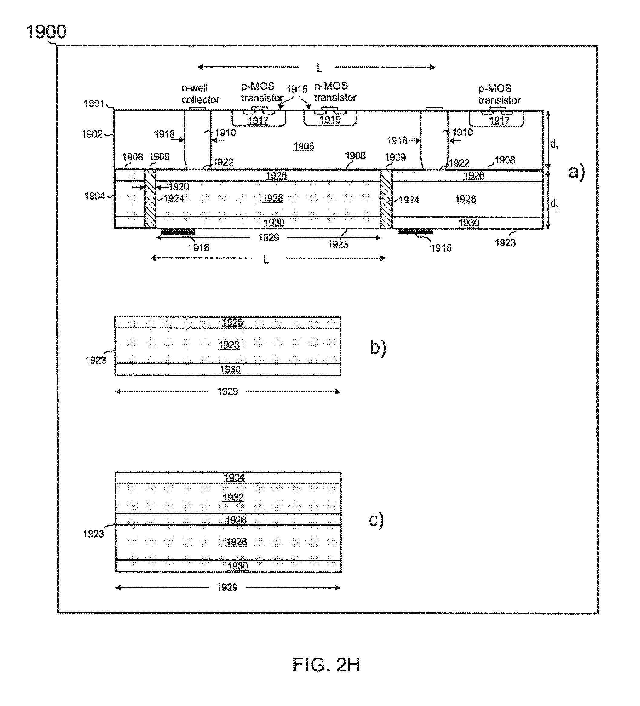
[0036] FIG. 2H is a schematic diagram showing a cross-section of a monolithic pixel detector of the invention with charge collection through covalent semiconductor bonds between mutually aligned n.sup.+-doped regions of a readout wafer and the pixels of a pixelated absorber wafer made up of p-i-n junctions or absorber and multiplication regions mutually isolated by insulating regions.
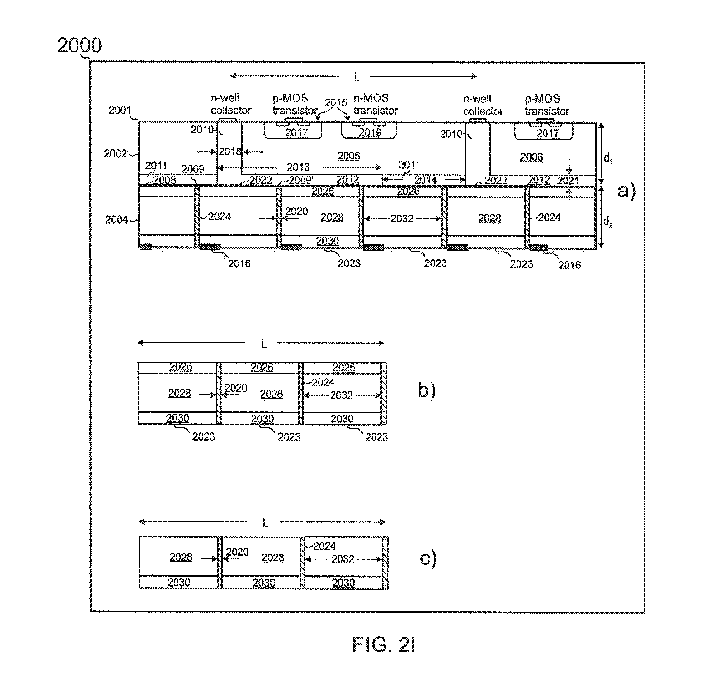
[0037] FIG. 2I is a schematic diagram showing a cross-section of a monolithic pixel detector of the invention with charge collection through covalent semiconductor bonds between n.sup.+-doped regions of a readout wafer and a pixelated absorber wafer made up of doped layers and pixels mutually isolated by insulating regions.
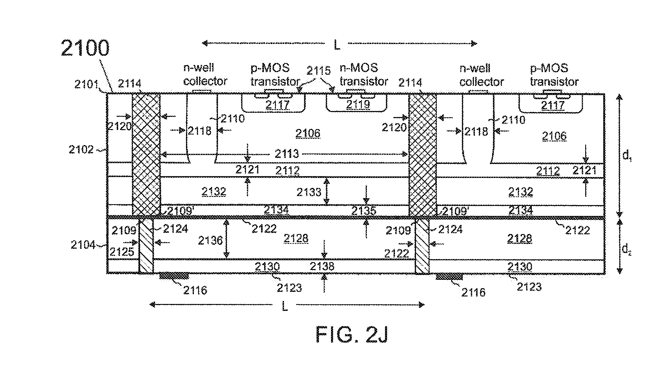
[0038] FIG. 2J is a cross-section of a monolithic pixel detector of the invention with charge collection both through covalent semiconductor bonds between a readout wafer containing multiplication regions and the pixels of a pixelated absorber wafer, wherein the pixels of readout and absorber wafers are mutually aligned and isolated by insulating regions.
[0039] FIG. 3A is a plan-view of the charge collectors of a monolithic pixel detector of the invention.
[0040] FIG. 3B is a plan-view of the charge collectors and the oxide regions surrounding the pixels of a monolithic pixel detector of the invention.
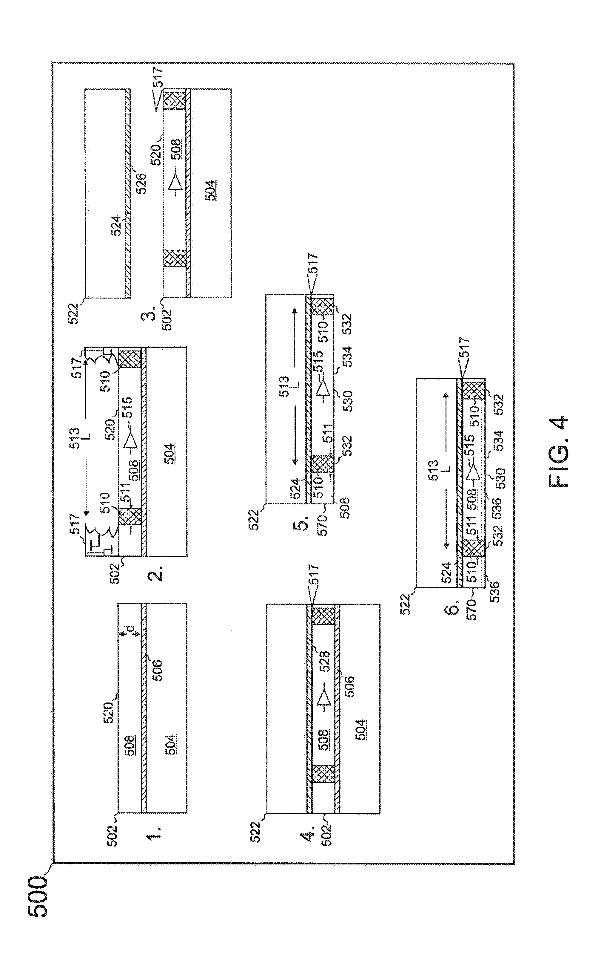
[0041] FIG. 4 is a schematic diagram showing the process flow of the invention for the fabrication of a thin readout wafer of the invention with highly doped charge collector plugs.
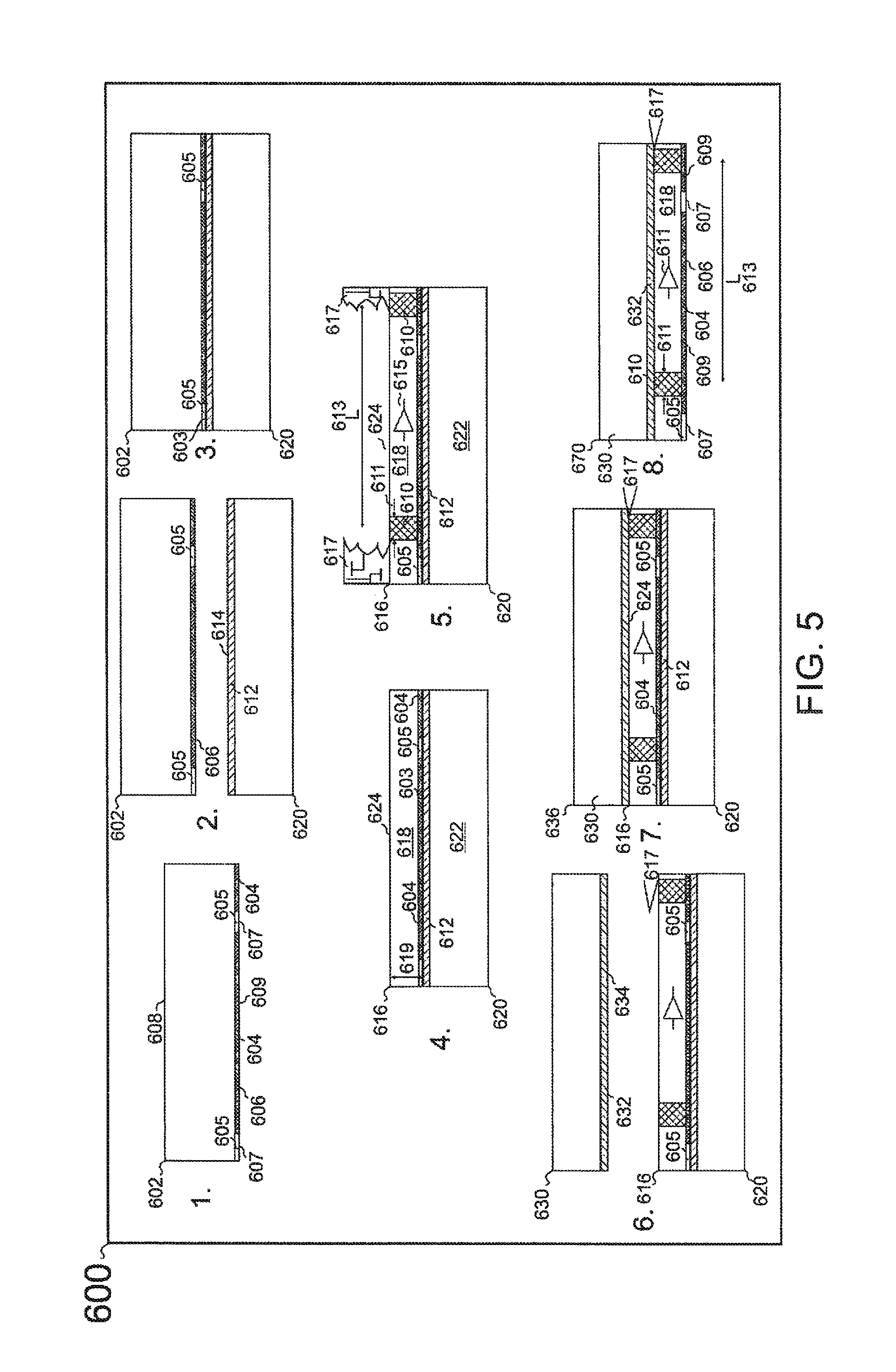
[0042] FIG. 5 is a schematic diagram showing the process flow of the invention for the fabrication of a thin readout wafer of the invention with highly doped charge collector plugs and implants.
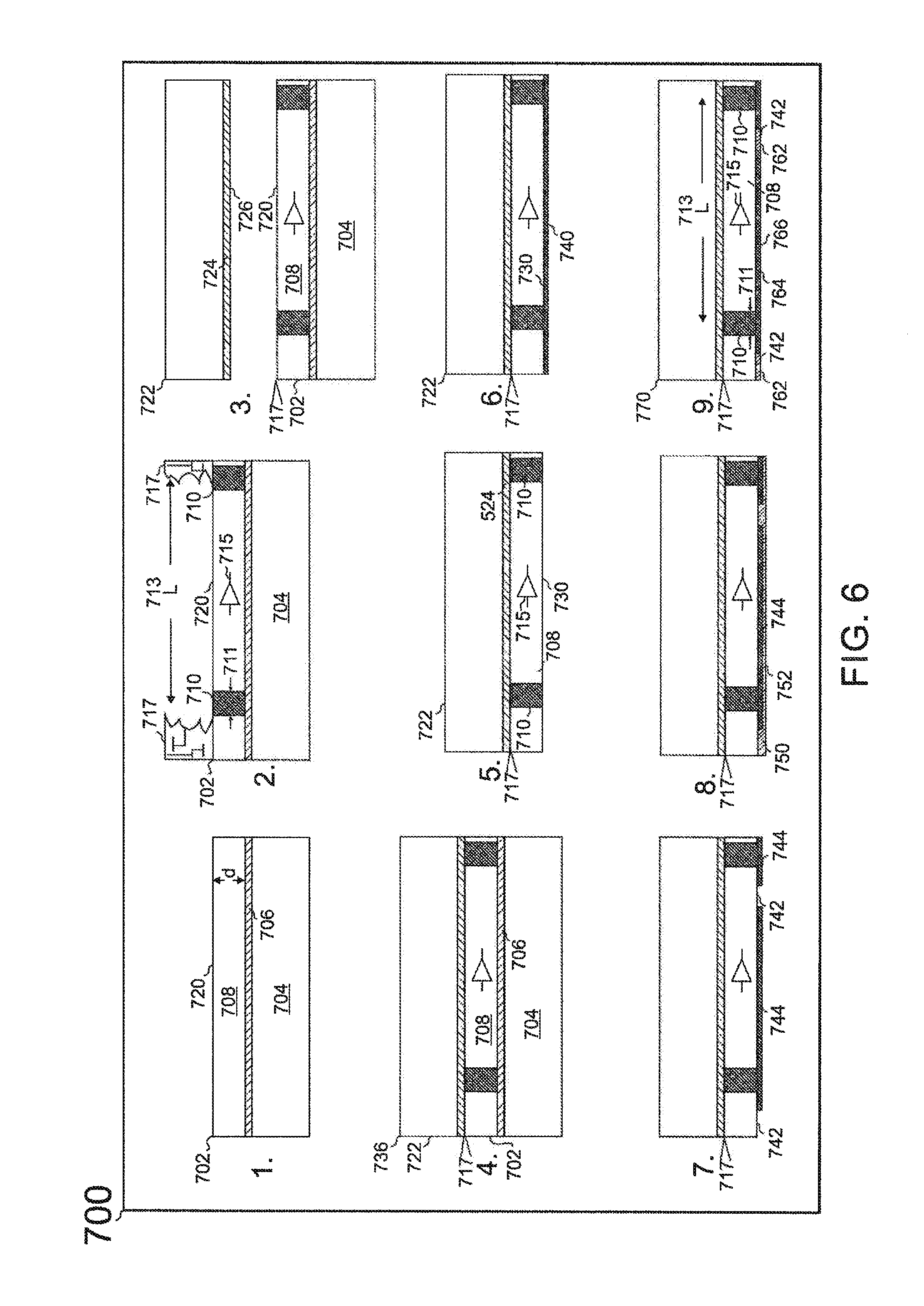
[0043] FIG. 6 is a schematic diagram showing the process flow of the invention for the fabrication of a thin readout wafer of the invention with metallic charge collector plugs and metal layers.
[0044] FIG. 7A is a schematic diagram showing the process flow of the invention for the fabrication of an absorber wafer of the invention made up of implants and oxide regions for pixel isolation.
[0045] FIG. 7B is a schematic diagram showing the process flow of the invention for the fabrication of an absorber wafer of the invention made up of metal regions along with oxide regions for pixel isolation.
[0046] FIG. 7C is a schematic diagram showing the process flow of the invention for the fabrication of an unpatterned absorber wafer of the invention.
[0047] FIG. 8 is a schematic diagram showing the process flow of the invention for the fabrication of an absorber wafer of the invention made up of epitaxial pillars with highly doped caps.
[0048] FIG. 9 is a schematic diagram showing the process flow of the invention for the fabrication of an absorber wafer of the invention made up of epitaxial pillars with highly doped caps, epilayer and oxide regions for pixel isolation.
[0049] FIG. 10 is a schematic diagram showing the process flow of a variant of the invention for the fabrication of an absorber wafer made up of epitaxial pillars with highly doped caps, metal layer and oxide regions for pixel isolation.
[0050] FIG. 11 a schematic diagram showing is the process flow of the invention for the fabrication of an absorber wafer of the invention with holes filled with epitaxial material.
[0051] FIG. 12A a schematic diagram showing is the process flow of the invention for the fabrication of a detector structure of the invention with a bonded absorber wafer.
[0052] FIG. 12B a schematic diagram showing is the process flow of the invention for the fabrication of a detector structure of the invention with a bonded unpatterned absorber wafer.
[0053] FIG. 12C a schematic diagram showing is the process flow of the invention for the fabrication of a detector structure of the invention with a bonded absorber wafer made up of holes filled with epitaxial material.
[0054] FIG. 13 is a schematic diagram showing a detector structure of the invention with epitaxial pillars bonded to highly doped regions of a thin readout wafer.
[0055] FIG. 14 is a schematic diagram showing a detector structure of the invention with highly doped regions on epitaxial pillars bonded to a thin readout wafer with highly doped regions.
[0056] FIG. 15 is a schematic diagram showing a detector structure of the invention with metallized epitaxial pillar regions bonded to metal regions on a thin readout wafer.
[0057] FIG. 16 is a schematic diagram showing a detector structure of the invention made up of epitaxial pillars on a thin substrate which is bonded to a thin readout wafer.
[0058] FIG. 17 is a schematic diagram showing the process flow of the invention for the fabrication of absorber pixels by aspect ratio trapping and their covalent bonding to a readout wafer.
[0059] FIG. 18 is a schematic diagram showing the process flow of the invention for the fabrication of absorber pixels by epitaxial growth on substrate pillars and their covalent bonding to a readout wafer.
[0060] FIG. 19A is a device for non-destructive testing using the pixel detectors of the invention in combination with a rotatable object for generating computed tomography images.
[0061] FIG. 19B is a device for non-destructive testing using an array of pixel detectors of the invention in combination with a static object for generating computed tomography images.
[0062] FIG. 20 is a vehicle equipped with an array of pixel detectors of the invention for collision control and tracking.
DETAILED DESCRIPTION OF THE PREFERRED EMBODIMENTS
[0063] It is the aim of this invention to provide simple structures and methods for the fabrication of sensitive pixel detectors for the detection of electromagnetic radiation, such as for example flat panel X-ray detectors with sizes up to about 20.times.20 cm.sup.2 or even about 40.times.40 cm.sup.2 and high-resolution detectors for the detection of infrared radiation. The detectors are composed of a readout unit processed in a thin CMOS wafer the backside of which is bonded to an absorber wafer, also called sensor wafer. These detectors are all configured for backside illumination, where electromagnetic radiation is incident on the absorber from the opposite side of the CMOS stack. The bonding happens on a wafer scale, and at least the bonds serving for charge collection are made between electrically highly conducting regions of the readout wafer and/or the absorber wafer, such as for example covalent semiconductor bonds between heavily doped semiconductors. The readout electronics is processed for example in an epitaxial Si layer with a thickness of about 10-30 .mu.m or preferably about 5-10 .mu.m or even 3-5 .mu.m and a resistivity above about 500 .OMEGA.cm or preferably about 1-2 k.OMEGA. cm or more preferably 2-5 k.OMEGA. cm or even above 5 k.OMEGA. cm, for example 5-50 k.OMEGA. cm, the resistivity being due to a low doping level in between about 10.sup.11 to 10.sup.13 cm.sup.-3 of a first conduction type (for example p-conduction induced by p-doping). For ease of detector manufacturing it may be advantageous to use silicon-on-insulator (SOI) wafers or epitaxial wafers made up of at least one epitaxial layer on a CZ or FZ wafer for the CMOS processing of the readout electronics. The use of such wafers may facilitate the thinning of the Si substrate of the CMOS wafer. The detectors can detect high-energy electromagnetic radiation in a single photon detection mode. Similar single photon detection capability may be achieved for example for infrared, visible or ultraviolet photons by incorporating an avalanche multiplication region into the monolithic detector structure. The sensor material can include any semiconductor available in the form of high purity wafers or in the faun of epitaxial layers grown on a substrate, whereby the substrate can for example be Si, Ge, GaAs, CdTe, a CdZnTe alloy or InSb, which may optionally be removed during detector fabrication. The thickness and the material used for the sensor strongly depend on the energy of the electromagnetic radiation which is to be detected. For the detection of low energy radiation from about one tenth of an eV up to a few keV, covering a spectral range from infrared to visible, ultraviolet and soft X-rays, a thickness on the order of one .mu.m or even less may be sufficient. There are many II/VI, III/V, IV/VI and group IV semiconductors covering this energy range, such as for example HgCdTe alloys, Pb salts, InSb, InGaAs alloys, Ge, Si, SiGe alloys, InP, GaAs, InGaN alloys, GaN, C (diamond), roughly in the order of increasing bandgap. As an example, for near infrared detection a Ge layer as thin as 0.5-1.5 .mu.m or even 0.3-0.5 .mu.m may be sufficient for efficient sensing up to a wavelength of about 1.6 .mu.m. Wafer bonding may be combined with wafer thinning, for example by hydrogen implantation and exfoliation (see for example I. P. Ferain et al., in J. Appl. Phys. 107, 054315 (2010), the entire disclosure of which is hereby incorporated by reference) or grinding and/or chemical etching. The sensitivity of infrared detectors may be further enhanced by incorporating an avalanche charge multiplication region communicating with the absorption region of the absorber wafer.
[0064] In the region between soft X-ray to hard X-ray detection, for example a SiC sensor with a thickness of about 3.5, 332 and 2310 .mu.m may absorb 90% of incident photons with energies of 2, 10 and 20 keV, respectively. A Si sensor with a thickness of about 3.9, 334 and 2330 .mu.m may absorb 90% of incident photons with energies of 2, 10 and 20 keV, respectively. For a Ge or GaAs sensor, the thickness necessary to absorb 90% of the incident photons with energy of 20, 30 and 40 keV is about 105, 320 and 710 .mu.m, respectively. For example a Si.sub.0.2Ge.sub.0.8 alloy would have to be about 25% thicker for the same absorption at these photon energies. Even harder X-rays of 40, 60 and 80 keV are absorbed to the same extent by a CdTe sensor or a CdZnTe alloy sensor whose thickness amounts to about 210, 610 and 1310 .mu.m, respectively (NIST X-ray attenuation data base, nist.gov/pml/data/ffast). The room temperature resistivity of intrinsic Ge is about 47 .OMEGA.cm and that of a Si.sub.0.25Ge.sub.0.75 alloy approximately 6.times.10.sup.4 .OMEGA.cm (see for example virginiasemi.com/pdf/generalpropertiesSi62002.pdf). X-ray detectors made up of Ge or SiGe absorbers therefore need to be cooled in order to lower dark leakage currents to acceptable levels for example of 1 nA per pixel or even between 10-100 pA. With respect to Ge and SiGe sensors, GaAs sensors have the advantage of much higher resistivity on the order of 10.sup.9 .OMEGA.cm (see for example M. C. Veale in Nucl Instr. Meth. Phys. Res, A 752, 6 (2014), the entire disclosure of which is hereby incorporated by reference). The same order of resistivity applies to CdTe sensors and even a higher one for CdZnTe alloy sensors (see for example S. Del Sordo et al. in Sensors 2009, 9, 3491-3526, the entire disclosure of which is hereby incorporated by reference).
[0065] The structures and methods of the invention refer to industrial scale wafers. High vacuum bonding equipment for 200 mm wafers is manufactured for example by EV Group (see for example C. Flotgen et al. in ECS Transactions 64, 103 (2014), the entire disclosure of which is hereby incorporated by reference).
[0066] For high-energy electromagnetic radiation, by its very construction, the monolithic pixel detectors of the invention offer single-photon detection. The monolithic X-ray pixel detectors of the invention are therefore suitable also for energy discrimination, whereby the energy of photons incident on the absorber can be measured by analysing the height of the electrical pulses processed by the readout electronics.
[0067] In contrast to prior art approaches (see for example U.S. Pat. No. 10,163,957 to von Kanel, and International Patent Application No. PCT/IB2017/001032 to von Kanel, the entire disclosures of which are hereby incorporated by reference) in the present invention charge carriers do not cross a bonding interface between lightly doped materials prior to arriving at charge collectors communicating with the readout electronics. The charges are instead channelled through bonding interfaces between electrically highly conducting regions where minority carrier generation and recombination does not occur. In all the following embodiments, the pixel detectors are configured for backside illumination, wherein electromagnetic radiation is incident on the absorber bonded on the backside of a thin silicon CMOS substrate with the CMOS stack on the opposite side, thereby offering fill factors close to 100%.
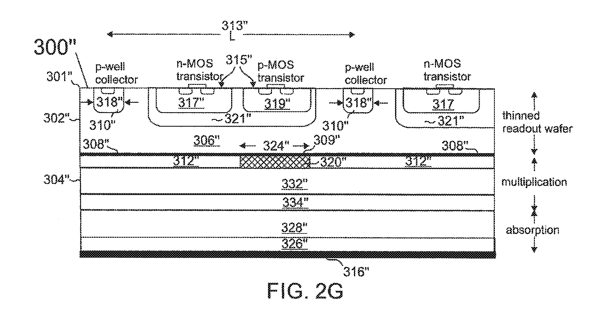
[0068] Referring now to FIG. 2A, first exemplary embodiment 100 of monolithic pixel detector 101 adapted to the detection of X-rays includes a bonding interface between thin readout wafer 102 of thickness d.sub.1 and absorber wafer 104 of thickness dz. The readout wafer is preferably fabricated for example by CMOS processing a weakly p-doped substrate 106 with a resistivity preferably of about 1-2 k.OMEGA. cm or even 2-5 k.OMEGA. cm which is thinned to a thickness of about 10-30 .mu.m or preferably about 5-10 .mu.m or even 3-5 .mu.m after all the processing has been completed. The thinning requires the planarization of the CMOS stack and the bonding of a carrier wafer before substrate 106 can be thinned. The bonding interface consists of conducting covalent semiconductor bond 108 between structures resembling silicon-through-vias 110 but filled with highly conducting n.sup.+-doped semiconductor material forming an n.sup.+-p junction with weakly p-doped substrate 106. In the following, these n.sup.+-doped vias, extending through substrate 106 will simply be called plugs 110. Plugs 110 form ohmic contacts with highly conducting n.sup.+-doped regions 112 in highly resistive p-conducting absorber wafer 104, which may for example be heavily doped implants. The doping level of highly conducting plugs 110 may for example be between 1.times.10.sup.18-1.times.10.sup.19 cm.sup.-3 or preferably 1.times.10.sup.19-1.times.10.sup.20 cm.sup.-3 or even 1.times.10.sup.20-5.times.10.sup.20 cm.sup.-3, corresponding to a resistivity between about 5-20 m.OMEGA. cm, 0.7-5 m.OMEGA. cm and 0.2-0.7 m.OMEGA. cm, respectively. Highly conducting regions 112 may have similar doping levels. Heavily doped plugs 110 may be formed for example by etching holes in lightly p-doped substrate 106 and their filling with n.sup.+-material in a subsequent epitaxy step known in the art. In another aspect of embodiment 100 a similar epitaxy process instead of implants 112 may result in heavily doped columns 124 doped to similar levels extending through most or all of absorber wafer 104. Optionally, absorber wafer 104 may further include heavily p-doped layer 117, facilitating ohmic contact formation with metallic back contact 116. Heavily doped plugs 110 bonded to heavily doped implants 112 or columns 124 serve as charge collectors, collecting electrons from electron-hole pairs which are generated by electromagnetic radiation incident on absorber wafer 104 and separated in the electric field of the reverse biased p-n junction 114, 126, formed by n.sup.+-doped regions 112, 124 and highly resistive p-conducting absorber wafer 104, upon applying a voltage to back contact 116 on absorber wafer 104. Minority carriers (electrons) thus never move across a bonding interface between low-doped wafers where trapping and recombination might occur. The charge collectors 110 communicate with the pixel readout electronics 115 of readout wafer 102 wherein the charge pulses generated by electromagnetic radiation are processed and forwarded to the off-pixel part of the readout electronics. The detector pixels are defined by the heavily doped plugs/regions 110/112, 110/124 the width 118, 119, 128 of which may for example range within about 0.5-2.5 .mu.m or preferably about 1-1.5 .mu.m. Width 118 of heavily doped plugs 110 in readout wafer 102 and width 119, 128 of heavily doped regions 112, 124 in absorber wafer 104 do not need to be equal but preferably at least one of them is in the range of at least 1-1.5 .mu.m to facilitate accurate alignment of wafers 102, 104 for bonding. In order to permit accurate alignment thin readout wafer 102 and absorber wafer 104 are both equipped with at least two special wafer alignment features in the form of alignment marks positioned for example close to the wafer edges on opposite sides. With the help of superimposing such alignment marks the rotational misalignment of 200 mm wafers may be kept within about (2-5).times.10.sup.-4 degrees and the lateral misalignment within about 0.5-1 .mu.m. Similar accuracy may be obtained in case of smaller wafer bonding. For example EVGroup offers an alignment tool with an accuracy below 1 .mu.m (see, e.g., evgroup.com/en/products/bonding/integrated_bonding/evg_combond, the entire disclosure of which is hereby incorporated by reference). The distance L between doped plugs 110 contacting regions 112/124 defines the pixel size 113 which can vary in a wide range within about 100-200 .mu.m, 50-100 .mu.m or 20-50 .mu.m or even 5-20 .mu.m. Using doped columns 124 instead of implants 112 has the advantage of easier depletion of absorber 104 at lower voltages applied to back contact 116 when the pixel size is smaller than the absorber thickness dz. Heavily doped implants 112 in absorber wafer 104 are surrounded by highly resistive regions 120 the resistivity of which is higher than that of implants 112 by at least a factor of 10.sup.4-10.sup.6. Regions 120 may even be insulating regions, such as oxide regions and form poorly conducting or electrically insulating semiconductor-to-oxide or oxide-to-oxide bond 122 between readout and absorber wafer the resistance of which is higher by at least a factor of 10.sup.2-10.sup.4, or preferably 10.sup.4-10.sup.6, or even more preferably 10.sup.6-10.sup.8 than that of bond 108. These highly resistive regions hence insulate the low-doped regions of readout wafer 102 (i.e. substrate 106) from low-doped, highly resistive absorber wafer 104, such that the only electrical connection between the two wafers is made between heavily doped regions 110 and 112, 124. At the same time regions 120 isolate adjacent pixels electrically from each other.
[0069] The pixel detector according to embodiment 100 is designed for detecting electrons from the electron-hole pairs generated by X-rays in absorber wafer 104. In an aspect of the embodiment the detector may be designed for hole collection by reversing the doping signs. The doping levels of p-doped regions may be about the same as the doping levels of n-doped regions discussed above. Somewhat higher doping by a factor of about 1.5 is needed for similar resistivity levels as for the n-doping case.
[0070] According to FIG. 2A, embodiment 100 requires precise mutual alignment of readout wafer 102 and absorber wafer 104 in order to form electrical contacts between heavily doped plugs 110 and heavily doped regions 112, 124.
[0071] The absorber wafer 104 may for example be a Si, SiC, Ge, GaAs, CdTe, or a CdZnTe alloy wafer obtained by bulk crystal growth. Alternatively, it may originate from at least one epitaxial layer of any of these materials on a single crystal substrate, which may optionally be removed after the covalent bonding step.
[0072] Referring now to FIG. 2B, second embodiment 100' of monolithic pixel detector 101' adapted to the detection of X-rays may include a bonding interface between thin readout wafer 102' of thickness d.sub.1' and absorber wafer 104' of thickness d.sub.2'. The readout wafer may have been fabricated for example by CMOS processing a weakly p-doped substrate 106' with a resistivity preferably of about 1-2 k.OMEGA. cm or even 2-5 k.OMEGA. cm which has a thickness d.sub.1' of about 10-30 .mu.m or preferably about 5-10 .mu.m or even 3-5 .mu.m. The thinning to such thicknesses may first require the planarization of the CMOS stack and the bonding of a carrier wafer to substrate 106'. Readout wafer 102' may contain highly conducting n.sup.+-doped plugs 110', extending through substrate 106' enclosed by highly resistive or insulating regions 120' the resistivity of which is higher than that of highly doped regions 110', 112' by at least a factor of 10.sup.4-10.sup.6. Highly resistive regions 120' may for example have been formed by local amorphization or local oxidation of wafer 102' before its bonding to highly resistive p-conducting absorber wafer 104'. Alternatively, for a resistivity of readout wafer 102' above about 2 k.OMEGA. cm, highly resistive regions 120' may not need to be especially formed. The doping level of highly conducting plugs 110' may for example be between 1.times.10.sup.18-1.times.10.sup.19 cm.sup.-3 or preferably 1.times.10.sup.19-1.times.10.sup.20 cm.sup.-3 or even 1.times.10.sup.20-5.times.10.sup.20 cm.sup.-3, corresponding to a resistivity between about 5-20 m.OMEGA. cm, 0.7-5 m.OMEGA. cm and 0.2-0.7 m.OMEGA. cm, respectively. Heavily doped plugs 110' may be formed for example by etching holes in lightly p-doped substrate 106' and their filling with n.sup.+-material in a subsequent epitaxy step known in the art. Absorber wafer 104' preferably contains heavily doped, highly conducting and unstructured surface layer 112', formed for example by ion implantation, which may have a similar doping type and doping level as plugs 110'. Optionally, absorber wafer 104' may further include heavily p-doped layer 117', facilitating ohmic contact formation with metallic back contact 116'. Heavily doped plugs 110' form ohmic contacts with heavily doped surface regions 112' of absorber wafer 104'. On the other hand, conducting surface layer 112' forms p-n junction 114' with the high resistivity, p-conducting bulk region of absorber wafer 104'. Heavily doped plugs 110' bonded to heavily doped regions 112' by conducting covalent semiconductor bonds 108', providing said ohmic contacts, serve as charge collectors, collecting electrons from electron-hole pairs which are generated by electromagnetic radiation incident on absorber wafer 104' and separated in the electric field of the reverse biased p-n junction 114', formed by heavily n-doped surface region 112' and p-conducting bulk region of absorber wafer 104', upon applying a voltage to back contact 116' on absorber wafer 104'. Electrons substantially do not, however, cross poorly conducting bonding interface 122' between highly resistive regions 120' of readout wafer 102' and doped regions 112' of absorber wafer 104' because its resistance exceeds that of conducting bonds by at least a factor of 10.sup.2-10.sup.4, or preferably 10.sup.4-10.sup.6, or even more preferably 10.sup.6-10.sup.8. Minority carriers (electrons) thus never move across a bonding interface between low-doped wafers where trapping and recombination might occur. Regions 120' therefore lead to pixel isolation and prevent the n-wells of the p-MOS transistors in pixel readout electronics 115' from acting as charge collectors along with n-doped plugs 110' which alone pick up the electrons generated by electromagnetic radiation in absorber wafer 104'. The charge collectors 110' communicate with the pixel readout electronics 115' of readout wafer 102' wherein the charge pulses generated by electromagnetic radiation are processed and forwarded to the off-pixel part of the readout electronics. The detector pixels are exclusively defined by the heavily doped plugs 110' in readout wafer 102', while absorber wafer 104' is unpatterned. The width 118' of plugs 110' should be substantially smaller than the pixel size 113' (for example by a factor of 5-10), the latter ranging within about 100-200 .mu.m, 50-100 .mu.m or 20-50 .mu.m or even 5-20 .mu.m. Width 118' may for example range within about 0.1-2.5 .mu.m.
[0073] The pixel detector according to embodiment 100' is designed for detecting electrons from the electron-hole pairs generated by X-rays in absorber wafer 104'. In an aspect of the embodiment the detector may be designed for hole collection by reversing appropriate doping signs. The doping levels of p-doped regions may be about the same as the doping levels of n-doped regions discussed above. Somewhat higher doping by a factor of about 1.5 is needed for similar resistivity levels as for the n-doping case.
[0074] According to its design (see FIG. 2B), made up of unpatterned absorber wafer 104', embodiment 100' does not require any precise alignment of readout wafer 102' and absorber wafer 104' in the bonding tool. It is sufficient to use approximate alignment as offered by superimposing wafer alignment features such as notches or flats supplied by wafer manufacturers which permit to keep the rotational misalignment of the two wafers within about 0.1 to 0.2 degrees, and the lateral displacement within about 200-400 .mu.m, as offered for example by the alignment and flipper module of the EVG580 ComBond tool. Embodiment 100' does not therefore require any additional alignment marks on readout and absorber wafer.
[0075] The absorber wafer 104' may for example be a Si, SiC, Ge, GaAs, CdTe, or a CdZnTe alloy wafer obtained by bulk crystal growth. Alternatively, it may originate from at least one epitaxial layer of any of these materials on a single crystal substrate, which may optionally be removed after the covalent bonding step.
[0076] Referring now to FIG. 2C, a third embodiment 200 of the monolithic pixel detector 201 adapted to the detection of X-rays may include a bonding interface between thin readout wafer 202 and absorber wafer 204. The readout wafer may have been fabricated for example by CMOS processing a weakly p-doped substrate 206 with a high resistivity preferably of about 1-2 k.OMEGA. cm or even 2-5 k.OMEGA. cm which is thinned to a thickness of about 10-30 .mu.m or preferably about 5-10 .mu.m or even 3-5 .mu.m after all the processing has been completed. The thinning may require the planarization of the CMOS stack and the bonding of a carrier wafer before substrate 206 can be thinned. Absorber wafer 204 is preferably highly resistive, lightly p-doped and may include highly conducting n.sup.+-doped regions 212 which may be a heavily doped implants or a heavily doped epitaxial layers. The doping level of highly conducting regions 212 may for example be between 1.times.10.sup.18-1.times.10.sup.19 cm.sup.-3 or preferably 1.times.10.sup.19-1.times.10.sup.20 cm.sup.-3 or even 1.times.10.sup.20-5.times.10.sup.20 cm.sup.-3, corresponding to a resistivity between about 5-20 m.OMEGA. cm, 0.7-5 m.OMEGA. cm and 0.2-0.7 m.OMEGA. cm, respectively. Optionally, absorber wafer 204 may further include heavily p-doped layer 217, facilitating ohmic contact formation with metallic back contact 216, The bonding interface may consist of conducting covalent semiconductor bond 208 between highly conducting n.sup.+-doped plugs 210 with similar doping levels extending through substrate 206 and conducting n.sup.+-doped regions 212 of the absorber wafer, thereby forming an ohmic contact, and poorly conducting covalent semiconductor bond 209 between the part of heavily doped regions 212 of the absorber wafer facing regions of low doped substrate 206. Poorly conducting covalent semiconductor bonds 209 have at least a 10.sup.2-10.sup.4, or preferably 10.sup.4-10.sup.6, or even more preferably 10.sup.6-10.sup.8 times higher resistivity than ohmic conducting bonds 208. Heavily doped plugs 210 may be formed for example by etching holes in lightly p-doped substrate 206 and their filling with n.sup.+-material in a subsequent epitaxy step known in the art. Heavily doped plugs 210 bonded to heavily n-doped regions 212 serve as charge collectors, collecting electrons from electron-hole pairs which are generated by electromagnetic radiation incident on absorber 204 and separated in the electric field of the reverse biased p-n junction 214 between n-doped regions 212 and the lightly p-doped bulk of wafer 204, upon applying a voltage to back contact 216 on absorber wafer 204. Minority carriers (electrons) thus never move across a poorly conducting bonding interface between low-doped wafers where trapping and recombination might occur. The charge collectors 210 communicate with the pixel readout electronics 215 of readout wafer 202 wherein the charge pulses generated by electromagnetic radiation are processed and forwarded to the off-pixel part of the readout electronics. The detector pixels are defined by the heavily doped plugs 210 the width 218 of which may for example range within about 0.5-2 .mu.m or preferably about 0.5-1 .mu.m. The distance L between plugs 210 defines the pixel size 213 which can vary in a wide range within about 100-200 .mu.m, 50-100 .mu.m or 20-50 .mu.m or even 5-20 .mu.m, Heavily doped regions 212 in absorber wafer 204 are surrounded by insulating oxide regions 220 forming substantially an electrically insulating semiconductor-to-oxide or oxide-to-oxide bond 222 between readout and absorber wafer with a resistance exceeding that of bond 208 by at least a factor of 10.sup.3-10.sup.4, or preferably 10.sup.4-10.sup.6, or even more preferably 10.sup.6-10.sup.8. The purpose of these oxide regions is to electrically isolate adjacent pixels from each other. Their width 224 may be smaller, equal or larger than width 226 of heavily doped regions 212 of absorber wafer 204, depending on the desired speed of pixel detector 200, which in turn depends on the size of the capacitor plate defined by width 226 of heavily doped region 212. Since width 226 of heavily doped regions 212 is preferably chosen to be larger that width 218 of heavily doped plugs 210, for example twice or three times as large or even as large as for example 90% of pixel size 213, the requirements for bonding alignment are more relaxed than in embodiment 100.
[0077] The pixel detector according to embodiment 200 is designed for detecting electrons from the electron-hole pairs generated by X-rays in absorber wafer 204. In an aspect of the embodiment the detector may be designed for hole collection by reversing the doping signs. The doping levels of p-doped regions may be about the same as the doping levels of n-doped regions discussed above. Somewhat higher doping by a factor of about 1.5 is needed for similar resistivity levels as for the n-doping case.
[0078] According to its design (see FIG. 2C), embodiment 200 requires precise mutual alignment of readout wafer 202 and absorber wafer 204 because oxide regions 220 in absorber wafer 204 are essentially spaced at pixel size 213 and serve as additional pixel isolation. Furthermore, heavily doped plugs 210 and heavily doped regions 212 need to be aligned in the bonding tool. In order to permit accurate alignment thin readout wafer 202 and absorber wafer 204 are both equipped with at least two special wafer alignment features in the form of alignment marks positioned for example close to the wafer edges on opposite sides. With the help of superimposing such alignment marks the rotational misalignment of 200 mm wafers may be kept below about 5.times.10.sup.-4 degrees and the lateral misalignment below 1 .mu.m. Similar accuracy may be obtained in case of smaller wafer bonding.
[0079] The absorber wafer 204 may for example be a Si, Sia Ge, GaAs, CdTe, or a CdZnTe alloy wafer obtained by bulk crystal growth. Alternatively, it may originate from at least one epitaxial layer of any of these materials on a single crystal substrate, which may optionally be removed after the covalent bonding step.
[0080] Referring now to FIG. 2D, fourth embodiment 200' of monolithic pixel detector 201' adapted to the detection of X-rays may include a bonding interface between thin readout wafer 202' and absorber wafer 204'. The readout wafer may have been fabricated for example by CMOS processing a weakly p-doped substrate 206' with a resistivity preferably of about 1-2 k.OMEGA. cm or even 2-5 k.OMEGA. cm which is thinned to a thickness of about 10-30 .mu.m or preferably about 5-10 .mu.m or even 3-5 .mu.m after all the processing has been completed. The thinning may require the planarization of the CMOS stack and the bonding of a carrier wafer before substrate 206' can be thinned. Absorber wafer 204' may include highly conducting n.sup.+-doped regions 212' which may be a heavily doped implants or a heavily doped epitaxial layers. The doping level of highly conducting regions 212' may for example be between 1.times.10.sup.18-1.times.10.sup.19 cm.sup.-3 or preferably 1.times.10.sup.19-1.times.10.sup.20 cm.sup.-3 or even 1.times.10.sup.20-5.times.10.sup.20 cm.sup.-3, corresponding to a resistivity between about 5-20 m.OMEGA. cm, 0.7-5 m.OMEGA. cm and 0.2-0.7 m.OMEGA. cm, respectively. Optionally, absorber wafer 204' may further include heavily p-doped layer 217', facilitating ohmic contact formation with metallic back contact 216'. The bonding interface may consist of conducting covalent semiconductor bond 208' between highly conducting n.sup.+-doped plugs 210' extending through substrate 206' and conducting n.sup.+-doped regions 212' of absorber wafer 204'. The doping level of plugs 210' is similar to that of regions 212', guaranteeing an ohmic contact between the two. The bonding interface between wafers 202', 204' furthermore includes poorly conducting covalent semiconductor bond 209' between the portion of heavily doped regions 212' of the absorber wafer facing regions of low doped substrate 206'. Poorly conducting covalent semiconductor bonds 209' have at least a 10.sup.2-10.sup.4, or preferably 10.sup.4-10.sup.6, or even more preferably 10.sup.6-10.sup.8 times higher resistivity than ohmic conducting bonds 208'. Heavily doped plugs 210', only one of which is shown in FIG. 2D, may be formed for example by etching holes in lightly p-doped substrate 206' and their filling with n.sup.+-material in a subsequent epitaxy step known in the art. Heavily doped plugs 210' bonded to heavily doped regions 212' form an ohmic contact between the two and serve as charge collectors, collecting electrons from electron-hole pairs which are generated by electromagnetic radiation incident on absorber 204' and separated in the electric field of the reverse biased p-n junction 214' between highly n-doped regions 212' and lightly p-doped substrate 206', upon applying a voltage to back contact 216' on absorber wafer 204'. Minority carriers (electrons) thus never move across a poorly conducting bonding interface between low-doped wafers where trapping and recombination might occur. The charge collectors 210' communicate with the pixel readout electronics 215' of readout wafer 202' wherein the charge pulses generated by electromagnetic radiation are processed and forwarded to the off-pixel part of the readout electronics. The detector pixels are defined by the heavily doped plugs 210' the width 218' of which may for example range within about 0.5-2 .mu.m or preferably about 0.5-1 .mu.m. The distance L between plugs 210' defines the pixel size 213' which can vary in a wide range within about 100-200 .mu.m, 50-100 .mu.m or 20-50 .mu.m or even 5-20 .mu.m. Heavily doped regions 212' in absorber wafer 204' are surrounded by oxide regions 220' of width 224' which may for example range within about 0.5-2 .mu.m or preferably about 0.5-1 .mu.m. Oxide regions 220' form electrically insulating oxide-to-oxide bonds 222' between absorber wafer 204' and oxide filled trenches 226' extending through readout wafer 202'. The width trenches 226' is preferably about the same as that of oxide regions 220'. Oxide regions 220', 226' isolate adjacent pixels from each other, and their spacing corresponds again to the pixel size L. Similar to embodiment 200 bonding alignment is facilitated here since heavily doped regions 212' cover most of pixel size 213'.
[0081] The pixel detector according to embodiment 200' is designed for detecting electrons from the electron-hole pairs generated by X-rays in absorber wafer 204'. In an aspect of the embodiment the detector may be designed for hole collection by reversing the appropriate doping signs. The doping levels of p-doped regions may be about the same as the doping levels of n-doped regions discussed above. Somewhat higher doping by a factor of about 1.5 is needed for similar resistivity levels as for the n-doping case.
[0082] According to its design (see FIG. 2D) embodiment 200' requires precise mutual alignment of readout wafer 202' and absorber wafer 204' for bonding, because oxide regions 220' in absorber wafer 204' and insulating oxide regions 226' of readout wafer 202' are essentially spaced at pixel size 213' and have to match during forming bonding interface 222'. Heavily doped plugs 210' and heavily doped regions 212' equally need to be aligned to form an ohmic contact at bonding interface 208'. In order to permit accurate alignment thin readout wafer 202' and absorber wafer 204' are both equipped with at least two special wafer alignment features in the form of alignment marks positioned for example close to the wafer edges on opposite sides. With the help of superimposing such alignment marks the rotational misalignment of 200 mm wafers may be kept within about (2-5).times.10.sup.-4 degrees and the lateral misalignment within about 0.5-1 .mu.m. Similar accuracy may be obtained in case of smaller wafer bonding.
[0083] The absorber wafer 204' may for example be a Si, SiC, Ge, GaAs, CdTe, or a CdZnTe alloy wafer obtained by bulk crystal growth. Alternatively, it may originate from at least one epitaxial layer of any of these materials on a single crystal substrate, which may optionally be removed after the covalent bonding step.
[0084] Referring now to FIG. 2E, fifth embodiment 300 of monolithic pixel detector 301 adapted to the detection of infrared radiation may include a bonding interface between thin readout wafer 302 and absorber wafer 304. The readout wafer may have been fabricated for example by CMOS processing p-doped substrate 306 with a resistivity between about 0.1-1 k.OMEGA. cm. Readout wafer 302 is thinned to a thickness of about 10-30 .mu.m or preferably about 5-10 .mu.m or even more preferably about 3-5 .mu.m after the processing of pixel electronics 315, made up of for example p-MOS transistors in n-wells 317 and n-MOS transistors in p-wells 319, has been completed. The thinning may require the planarization of the CMOS stack and the bonding of a carrier wafer before substrate 306 can be thinned. Preferably, readout wafer 302 contains heavily n-doped, highly conducting regions 312 enclosed by highly resistive regions 320, the latter serving for mutual electrical pixel isolation. The doping of regions 312 may for example be between 1.times.10.sup.18-1.times.10.sup.19 cm.sup.-3 or preferably 1.times.10.sup.19-1.times.10.sup.20 cm.sup.-3 or even 1.times.10.sup.20-5.times.10.sup.20 cm.sup.-3, corresponding to a resistivity between about 5-20 m.OMEGA. cm, 0.7-5 m.OMEGA. cm and 0.2-0.7 m.OMEGA. cm, respectively. The resistivity of highly resistive regions 320 may be higher by at least a factor of about 10.sup.2-10.sup.4, or preferably 10.sup.4-10.sup.6, or even more preferably 10.sup.6-10.sup.8 with respect to that of highly conducting regions 312. Regions 312 and 320 may for example be formed by ion implanting thin SOT wafers by dopants or oxygen, respectively, before the low doped substrate 306 is epitaxially grown by chemical vapour deposition. Alternatively, heavily doped regions 312 and high resistivity regions 320 may also be formed by backside processing after thinning of readout wafer 302. Heavily doped regions 312 may form ohmic contacts 322 with highly conducting n.sup.+-doped plugs 310 which have similar doping levels and extend through low doped substrate 306. Absorber wafer 304 may optionally include unpatterned, highly conducting n-doped layer 326, which may be a heavily doped implant or a heavily doped epitaxial layer, forming highly conducting covalent semiconductor bond 308 with heavily doped regions 312 of readout wafer 302. The doping level of doped layer 326 may for example be between 1.times.10.sup.18-1.times.10.sup.19 cm.sup.-3 or preferably 1.times.10.sup.19-1.times.10.sup.20 cm.sup.-3 or even 1.times.10.sup.20-5.times.10.sup.20 cm.sup.-3. The part of layer 326 facing highly resistive regions 320 may either form a poorly conducting covalent semiconductor or a semiconductor-to-insulator bond 309, depending on whether regions 320 are highly resistive semiconductor regions or insulator regions, such as for example oxide regions. In any case the resistance of bond 309 exceeds that of bond 308 by at least a factor of 10.sup.2-10.sup.4, or preferably 10.sup.4-10.sup.6, or even more preferably 10.sup.6-10.sup.8. Absorber 304 may further include low-doped infrared absorption layer 328 next to layer 326 and a stack of layers made up of a p-i-n diode or avalanche diode with n-doped charge region 330, intrinsic or highly resistive p.sup.--doped charge multiplication layer 332 and heavily p-doped anode region 334.
[0085] In the design of embodiment 300, doped plugs 310 contacting doped regions 312 serve as charge collectors, collecting electrons generated for example by avalanche breakdown, when holes produced by infrared radiation incident on absorption layer 328 give rise to an avalanche current in charge multiplication layer 332 while the detector is in operation and a reverse bias above the breakdown voltage V.sub.B is applied to transparent back contact, such as a conductive oxide contact (e.g., indium-tin-oxide or zinc oxide) or pixelated metal back contact 316. In this so-called Geiger mode of operation, the detector is suitable for single photon detection (single photon avalanche detector or SPAD) similar to the X-ray detectors of embodiments 100-200'. The doping levels of layers 328, 330, 332 and 334 is preferably chosen to assure the highest electric field to be present in charge multiplication layer 332, while the field in absorption layer 328 is just large enough to cause holes to drift into the charge multiplication region. Hence the doping of layer 328 may for example be 10.sup.14-10.sup.15 cm.sup.-3, that of layer 330 about 5.times.10.sup.16-5.times.10.sup.17 cm.sup.-3, that of layer 332 about 5.times.10.sup.14-5.times.10.sup.15 cm.sup.-3, and finally that of layer 334 about 10.sup.19-10.sup.20 cm.sup.-3. Similar to the embodiments adapted for X-ray detection charge collectors 310 communicate with the pixel readout electronics 315 of readout wafer 302 which further includes quenching circuits designed for lowering the bias below V.sub.B (see for example F. Zappa et al. in Sensors and Actuators A 140,103 (2007), the entire enclosure of which is hereby incorporated by reference). The detector pixels are defined by the heavily doped plugs 310 the width 318 of which may for example range within about 0.1-2 .mu.m or preferably about 0.5-1 The distance L between plugs 310 defines the pixel size 313 which can for example vary in a range within about 2-40 .mu.m or preferably about 2-20 .mu.m or even more preferably about 2-5 .mu.m.
[0086] In the design of embodiment 300, absorption layer 328 is a semiconductor layer with a lower bandgap with respect to the one of charge multiplication layer 332. Layer 328 may for example be nearly intrinsic Ge layer or a low doped layer with a doping density preferably below about 10.sup.15 cm.sup.-3 and a thickness of about 1 .mu.m. Detectors with a Ge absorption layer are typically suitable for detecting infrared photons from a wavelength of about 0.8 .mu.m to about 1.6 .mu.m. Charge region 330 may be an n-doped GaAs layer with a doping density in the range of about 1-5.times.10.sup.17 cm.sup.-3 and a thickness around 0.1 .mu.m. Multiplication layer 332 may be a low n-doped GaAs layer with a doping density of about 10.sup.15 cm.sup.-3 and a thickness in the range of 0.5-2 .mu.m. Layer 334 may finally be a heavily p-doped GaAs layer with a doping level of about 5.times.10.sup.19 cm.sup.-3 and a thickness of 0.1-0.2 .mu.m. An absorber wafer made up of such a layer stack can for example advantageously be made by growing the GaAs layers epitaxially on a Ge substrate wafer to which they are very closely lattice matched. Before forming wafer bonds 308, 309 the Ge substrate wafer has to be thinned, for example by first bonding the epitaxial GaAs surface to a carrier wafer, and then thinning the Ge substrate wafer by grinding and chemical mechanical planarization (CMP) or by layer splitting as known in the art (see for example I. P. Ferain et al. in J. Appl. Phys. 107, 054315 (2010), the entire disclosure of which is hereby incorporated by reference).
[0087] As is evident from FIG. 2E, pixel detector 301 offers a fill factor close to 100%. Furthermore, according to its design (see FIG. 2E), made up of unpatterned absorber wafer 304, the infrared detector 301 of embodiment 300 does not require any precise alignment of readout wafer 302 and absorber wafer 304 in the bonding tool similar to embodiment 100' for a pixel detector adapted to X-ray detection. It is sufficient to use approximate alignment as offered by superimposing wafer alignment features such as notches or flats supplied by wafer manufacturers which permit to keep the rotational misalignment of the two wafers within about 0.1 to 0.2 degrees, and the lateral displacement within about 200-400 .mu.m, as offered for example by the alignment and flipper module of the EVG580 ComBond tool. Embodiment 300 does not therefore require any additional alignment marks on readout and absorber wafer. Similar to the X-ray detectors of embodiments 100-200' the infrared detector of embodiment 300 may have single photon detection capability when it is operated in Geiger mode (see for example F. Zappa et al. in Sensors and Actuators A 140,103 (2007), the entire enclosure of which is hereby incorporated by reference).
[0088] The pixel detector according to embodiment 300 is designed for detecting electrons from the electron-hole pairs in avalanche layer 332. In an aspect of the embodiment the detector may be designed for hole collection by reversing the appropriate doping signs. The doping levels of p-doped regions may be about the same as the doping levels of n-doped regions discussed above. Somewhat higher doping by a factor of about 1.5 is needed for similar resistivity levels as for the n-doping case.
[0089] Referring now to FIG. 2F, sixth embodiment 300' of monolithic pixel detector 301' adapted to the detection of infrared radiation may include two bonding interfaces. First, highly conducting, bonding interface 308' lies between thin Si readout wafer 302' and second thin Si wafer 303', made up of Si multiplication layer 332'. Second bonding interface 314' lies between second thinned Si wafer 303' and absorber layer stack 305' which together form absorber wafer 304'.
[0090] The readout wafer may have been fabricated for example by CMOS processing p-doped substrate 306' with a resistivity between about 0.1-1 k.OMEGA. cm. Readout wafer 302' is thinned to a thickness of about 10-30 .mu.m or preferably about 5-10 .mu.m or even more preferably about 3-5 .mu.m after the processing of pixel electronics 315', made up of for example p-MOS transistors in n-wells 317' and n-MOS transistors in p-wells 319', has been completed. The thinning may require the planarization of the CMOS stack and the bonding of a carrier wafer before substrate 306' can be thinned. Likewise, the thinning of second Si wafer 303' may require carrier wafer bonding before the thinning, unless a layer splitting technique is used after forming first bonding interface 308'. Preferably, readout wafer 302' contains heavily n-doped, highly conducting regions 312' enclosed by highly resistive regions 320' the latter serving for mutual electrical pixel isolation. The doping of regions 312' may for example be between 1.times.10.sup.18-1.times.10.sup.19 cm.sup.-3 or preferably 1.times.10.sup.19-1.times.10.sup.20 cm.sup.-3 or even 1.times.10.sup.20-5.times.10.sup.20 cm.sup.-3, corresponding to a resistivity between about 5-20 m.OMEGA. cm, 0.7-5 m.OMEGA. cm and 0.2-0.7 m.OMEGA. cm, respectively. The resistivity of highly resistive regions 320' is higher by at least a factor of about 10.sup.2-10.sup.4 or 10.sup.4-10.sup.6, or even 10.sup.6-10.sup.8 with respect to that of highly conducting regions 312' and the resistance of bond 309' exceeds that of bond 308' by at least a factor of 10.sup.2-10.sup.4, or preferably 10.sup.4-10.sup.6, or even more preferably 10.sup.6-10.sup.8. Regions 312' and 320' may for example be formed by ion implanting thin SOI wafers before the low doped substrate 306' is epitaxially grown by chemical vapour deposition by dopant atoms or oxide atoms, respectively. Heavily doped regions 312' may form ohmic contacts 322' with the highly conducting regions of n.sup.+-doped plugs 310' which have similar doping levels and extend through low doped substrate 306'. Covalent semiconductor bond 314' is formed between infrared absorption layer 328' of absorber layer stack 305' and charge layer 334' of second thinned Si wafer 303'. A silicon p-i-n or avalanche diode is formed between heavily doped regions 312' of readout wafer 302' which is bonded to highly resistive, intrinsic or very low doped charge multiplication region 332' of second, thin Si wafer 303' in highly conducting covalent semiconductor bond 308', and p-doped charge layer 334'. In an aspect of the embodiment the entire Si charge multiplication region may be part of readout wafer 302'. In this aspect of the embodiment, first regions 312', 320', 332', 334' may be formed by processing a Si wafer, for example by epitaxial growth and/or ion implantation. Subsequently, epitaxial layer 306' may be grown by CVD and then CMOS processed to create pixel readout electronics 315' along with charge collectors 318'. In this case bonding of thin Si wafer 303' is not required. There is in this case only one single covalent semiconductor bond 314' present between. Si readout wafer 302' and infrared absorption layer 328' of absorber layer stack 305'. In the design of embodiment 300', doped plugs 310' contacting doped regions 312' serve as charge collectors, collecting electrons generated for example by avalanche breakdown, when electrons produced by infrared radiation incident on absorption layer 328' give rise to an avalanche current in multiplication layer 332' while the detector is in operation and a reverse bias above the breakdown voltage V.sub.B is applied to transparent back contact, such as a conductive oxide contact (e.g., indium-tin-oxide or zinc oxide) or pixelated metal back contact 316'. In this so-called Geiger mode of operation, the detector becomes a single photon avalanche detector (SPAD). The doping levels of layers 328', 332' and 334' is preferably chosen to assure the highest electric field to be present in multiplication layer 332', while the field in absorption layer 328' is just large enough to cause electrons to drift into the charge multiplication region. Hence the doping of absorption layer 328' may for example be 10.sup.14-10.sup.15 cm.sup.-3, that of charge layer 334' about 5.times.10.sup.16-5.times.10.sup.17 cm.sup.-3, that of charge multiplication layer 332' about 5.times.10.sup.14-5.times.10.sup.15 cm.sup.-3, and finally that of layer 334 about 10.sup.19-10.sup.20 cm.sup.-3. Similar to the embodiments adapted for X-ray detection charge collectors 310' communicate with the pixel readout electronics 315' of readout wafer 302' which further includes quenching circuits designed for lowering the bias below V.sub.B (see for example F. Zappa et al. in Sensors and Actuators A 140,103 (2007), the entire enclosure of which is hereby incorporated by reference). The detector pixels are defined by the heavily doped plugs 310' the width 318' of which may for example range within about 0.1-2 .mu.m or preferably about 0.5-1 .mu.m. The distance L between plugs 310' defines the pixel size 313' which can for example vary in a range within about 2-40 .mu.m or preferably about 2-20 .mu.m or even more preferably about 2-5 .mu.m.
[0091] In the design of embodiment 300', absorption layer 328' is a semiconductor layer with a lower bandgap with respect to the one of Si multiplication layer 332'. Layer 328' may for example be nearly intrinsic Ge layer or a low doped layer with a doping density preferably below about 10.sup.15 cm.sup.-3, for example 10.sup.14-10.sup.15 cm.sup.-3 and a thickness of about 1 .mu.m. Detectors with a Ge absorption layer are typically suitable for detecting infrared photons from a wavelength of about 0.8 .mu.m to about 1.6 .mu.m. Charge layer 334' may have a doping density in the range of about 5.times.10.sup.16-5.times.10.sup.17 cm.sup.-3 and a thickness around 0.1 .mu.m. The Si multiplication layer 332' may have a doping density of about 5.times.10.sup.14-5.times.10.sup.15 cm.sup.-3 and a thickness in the range of 0.5-2 .mu.m. Optional layer 326' of absorber wafer 304' may finally be a heavily p-doped Ge layer with a doping level of about 1.times.10.sup.19-1.times.10.sup.20 cm.sup.-3 and a thickness of 0.5-1 .mu.m facilitating ohmic contact formation with back contact 316'. Preferably, second thinned Si wafer 303' is made from an SOI wafer, which facilitates its thinning after bonding to thinned readout wafer 302'. Ge absorption wafer 304' may on the other hand be thinned after bonding by grinding and CMP or by layer splitting as known in the art (see for example I. P. Ferain et al. in J. Appl. Phys. 107, 054315 (2010), the entire disclosure of which is hereby incorporated by reference). The process of forming wafer bonds 308', 309', 314', or single wafer bond 314' in case of an aspect of the embodiment, before wafer thinning has the advantage that no carrier wafer bonding is needed for carrying out these steps.
[0092] As is evident from FIG. 2F, pixel detector 301' offers a fill factor close to 100%. Furthermore, according to its design (see FIG. 2F) which includes the bonding of unpatterned Si wafer 303' to thin readout wafer 302', infrared detector 301' of embodiment 300' does not require any precise alignment of these wafers in the bonding tool. Neither does absorber layer stack 305' need to be precisely aligned with thinned Si wafer 303' for bonding. It is sufficient to use approximate alignment as offered by superimposing wafer alignment features such as notches or flats supplied by wafer manufacturers which permit keeping the rotational misalignment of the two wafers within about 0.1 to 0.2 degrees, and the lateral displacement within about 200-400 .mu.m, as offered for example by the alignment and flipper module of the EVG580 ComBond tool. Embodiment 300' does not therefore require any additional alignment marks on readout and absorber wafer. Similar to embodiment 300 embodiment 300' may provide single photon detection capability when it is operated in Geiger mode (see for example F. Zappa et al. in Sensors and Actuators A 140,103 (2007), the entire enclosure of which is hereby incorporated by reference).
[0093] Referring now to FIG. 2G, seventh embodiment 300'' of monolithic pixel detector 301'' adapted to the detection of infrared radiation may include a bonding interface between thin readout wafer 302'' and absorber wafer 304''.
[0094] The readout wafer may have been fabricated for example by CMOS processing p-doped substrate 306'' with a resistivity between about 0.1-1 k.OMEGA. cm. Readout wafer 302'' is thinned to a thickness of about 10-30 .mu.m or preferably about 5-10 .mu.m or even more preferably about 3-5 .mu.m after the processing of pixel electronics 315'', made up of for example p-MOS transistors in n-wells 317'' and n-MOS transistors in p-wells 319'' and additional deep n-wells 321'', has been completed. The thinning may require the planarization of the CMOS stack and the bonding of a carrier wafer before substrate 306'' can be thinned. Readout wafer 302'' may contain highly conducting, heavily p-doped implants 310'' adapted for hole collection. In contrast to the electron collectors 310, 310' of embodiments 300, 300', hole collectors 310'' do not need to extend through the whole thickness of the readout wafer. Deep n-wells 321'' prevent p-wells 319'' from collecting holes. The doping of implants 310'' may for example be between 1.times.10.sup.18-1.times.10.sup.19 cm.sup.-3 or preferably 1.times.10.sup.19-1.times.10.sup.20 or even 1.times.10.sup.20-5.times.10.sup.20 cm.sup.-3, corresponding to a resistivity between about 5-20 m.OMEGA. cm, 0.7-5 m.OMEGA. cm and 0.2-0.7 m.OMEGA. cm, respectively. The bonding interface between readout wafer 302'' and absorber wafer 304'' may consist of covalent semiconductor bond 308'' between low p-doped Si substrate 306'' and highly conducting, heavily p-doped layer 312'' and of bond 309'', which may be a poorly conducting covalent semiconductor or a semiconductor-to-insulator bond depending on whether regions 320'', which electrically isolate neighbouring pixels, are highly resistive semiconductor regions or insulator regions, such as for example oxide regions. In any case, the resistivity of highly resistive regions 320'' is higher by at least a factor of about 10.sup.2-10.sup.4, or even 10.sup.4-10.sup.6, or as much as 10.sup.6-10.sup.8 with respect to that of highly conducting regions 312'' leading to a resistance of bond 309'' exceeding that of bond 308'' by at least a factor of 10.sup.2-10.sup.4, or preferably 10.sup.4-10.sup.6, or even more preferably 10.sup.6-10.sup.8. Absorber wafer 304'' may further include very weakly n-doped or intrinsic charge multiplication layer 332'' and more highly n-doped charge layer 334''. A p-i-n or avalanche diode is thereby formed between heavily p-doped regions 312'', intrinsic or very low doped charge multiplication region 332'' and n-doped charge layer 334''. Adjacent to said p-i-n diode absorber wafer 304'' may further include intrinsic or preferably lightly p-doped absorption layer 328'' and finally optional heavily doped layer 326'', which facilitates ohmic contact formation with back contact 316''.
[0095] In the design of embodiment 300'', p-doped implants 310'' may hence serve as hole collectors generated for example by avalanche breakdown, when holes produced by infrared radiation incident on absorption layer 328'' give rise to an avalanche current in multiplication layer 332'', when the detector is in operation and a reverse bias above the breakdown voltage V.sub.B is applied to transparent back contact, such as a conductive oxide contact (e.g., indium-tin-oxide or zinc oxide) or pixelated metal back contact 316''. In this so-called Geiger mode of operation single photons can be detected (single photon avalanche detector, SPAD). The doping levels of layers 328'', 332'' and 334'' are preferably chosen to assure the highest electric field to be present in multiplication layer 332'', while the field in absorption layer 328'' is just large enough to cause holes to drift into the multiplication region. Similar to the embodiments 300, 300' charge collectors 310'' communicate with the pixel readout electronics 315'' of readout wafer 302'' which further includes quenching circuits designed for lowering the bias below V.sub.B (see for example F. Zappa et al. in Sensors and Actuators A 140,103 (2007), the entire enclosure of which is hereby incorporated by reference). The detector pixels are defined by the heavily doped implants 310'' the width 318'' of which may for example range within about 0.1-2 .mu.m or preferably about 0.5-1 .mu.m. The distance L between implants 310'' defines the pixel size 313'' which can for example vary in a range within about 2-40 .mu.m or preferably about 2-20 .mu.m or even more preferably about 2-5 .mu.m.
[0096] In the design of embodiment 300'', absorption layer 328'' is a semiconductor layer with a lower bandgap with respect to the semiconductor from which charge multiplication layer 332'' and layers 312'', 334'' are made. Layer 328'' may for example be nearly intrinsic Ge layer or a low doped layer with a doping density preferably below about 10.sup.15 cm.sup.-3, for example 10.sup.14-10.sup.15 cm.sup.-3, and a thickness of about 1 .mu.m. Detectors with a Ge absorption layer are typically suitable for detecting infrared photons from a wavelength of about 0.8 .mu.m to about 1.6 .mu.m. Charge layer 334'', multiplication layer 332'' and heavily p-doped layer 312'' may for example be GaAs layers. Layers 312'' may for example be doped to a level between 1.times.10.sup.18-1.times.10.sup.19 cm.sup.-3 or preferably 1.times.10.sup.19-1.times.10.sup.20 cm.sup.-3 or even 1.times.10.sup.20-5.times.10.sup.20 cm.sup.-3. Charge layer 334'' may have an n-doping density in the range of about 1-5.times.10.sup.17 cm.sup.-3 and a thickness around 0.1 .mu.m. Multiplication layer 332'' may have a n.sup.--doping density of about 10.sup.15 cm.sup.-3 and a thickness in the range of 0.5-2 .mu.m. Optional layer 326'' of absorber wafer 304'' may finally be a heavily n-doped Ge layer with a doping level of about (1-5).times.10.sup.19 cm.sup.-3 and a thickness of 0.1-0.2 .mu.m facilitating ohmic contact formation with back contact 316''. An absorber wafer made up of such a layer stack can for example advantageously be made by growing the GaAs layers epitaxially on a Ge substrate wafer to which they are very closely lattice matched. Ge absorption wafer 304'' may be thinned after bonding by grinding and CMP or by layer splitting as known in the art (see for example I. P. Ferain et al. in J. Appl. Phys. 107, 054315 (2010), the entire disclosure of which is hereby incorporated by reference). The process of forming wafer bonds 308', 309' before wafer thinning has the advantage that no carrier wafer bonding is needed for carrying out these steps.
[0097] As is evident from FIG. 2G pixel detector 301'' offers a fill factor close to 100%. Furthermore, according to its design (see FIG. 2G), embodiment 300'' requires precise mutual alignment of readout wafer 302'' and absorber wafer 304'' for bonding, because insulating regions 320'' in absorber wafer 304'' are essentially spaced at pixel size 313'' and have to be positioned between implants 310'' during wafer bonding. In order to permit accurate alignment thin readout wafer 302'' and absorber wafer 304'' are both equipped with at least two special wafer alignment features in the form of alignment marks positioned for example close to the wafer edges on opposite sides. With the help of superimposing such alignment marks the rotational misalignment of 200 mm wafers may be kept within about (2-5).times.10.sup.-4 degrees and the lateral misalignment within about 0.2-1 .mu.m or even about 0.1-0.2 .mu.m. Similar accuracy may be obtained in case of smaller wafer bonding.
[0098] Similar to embodiment 300, embodiment 300'' may provide single photon detection capability when it is operated in Geiger mode (see for example F. Zappa et al. in Sensors and Actuators A 140,103 (2007), the entire enclosure of which is hereby incorporated by reference).
[0099] Referring now to FIG. 2H, eighth embodiment 1900 of monolithic pixel detector 1901 adapted to the detection of infrared radiation may include a bonding interface made up of bonds 1908, 1909, 1922 between thin readout wafer 1902 and pixelated absorber wafer 1904 in the form of absorber patches 1923, The readout wafer 1902 may have been fabricated for example by CMOS processing p-doped substrate 1906 with a resistivity between about 0.1-1 k.OMEGA. cm. The substrate of readout wafer 1902 is thinned from the back to a thickness d.sub.1 of about 10-30 .mu.m or preferably about 5-10 .mu.m or even more preferably about 3-5 .mu.m after the processing of pixel electronics 1915, made up of for example p-MOS transistors in n-wells 1917 and n-MOS transistors in p-wells 1919, has been completed. In order to be bondable, the thinning must include a chemical mechanical planarization step resulting in an RMS surface roughness typically below 0.5 nm or preferably 0.1 to 0.3 nm. The thinning of readout wafer 1902 may further require the planarization of the CMOS stack and the temporary bonding of a carrier wafer before substrate 1906 can be thinned. Readout wafer 1902 contains heavily n-doped, highly conducting charge collectors 1910 of width 1918 of about 0.1-2 .mu.m or preferably about 0.3-0.8 .mu.m and for which the spacing L corresponds to the pixel size. The doping of charge collectors 1910 may for example be between 1.times.10.sup.18-1.times.10.sup.19 cm.sup.-3 or preferably 1.times.10.sup.19-1.times.10.sup.20 cm.sup.-3 or even 1.times.10.sup.20-5.times.10.sup.20 cm.sup.-3, corresponding to a resistivity between about 5-20 m.OMEGA. cm, 0.7-5 m.OMEGA. cm and 0.2-0.7 m.OMEGA. cm, respectively. Absorber wafer 1904 is pixelated with absorber patches 1923 of a characteristic width 1929 mutually isolated by insulating regions 1924 of a characteristic width 1920 and spaced at the pixel size L of the detector. Preferably, insulating regions 1924 extend across the entire thickness d.sub.2 of the absorber wafer 1904 and have a width 1920 of about 0.1 to 2 .mu.m or preferably about 0.1 to 1 .mu.m. If made from metal, back contacts 1916 for the application of a reverse bias V.sub.b may be chosen to extend only along a small fraction of the width 1929 of absorber patches 1923 to minimize the blocking of electromagnetic radiation. Alternatively, contacts 1916 may cover the entire area of absorber patches 1923 if they are made for example from a transparent (to the electromagnetic radiation to be detected) conductive oxide such as indium-tin-oxide or zinc oxide. The pixel size L can vary for example in a range of about 2-40 .mu.m or preferably about 2-20 .mu.m or even more preferably about 2-5 .mu.m.
[0100] In a first aspect of the embodiment (see FIG. 2H a) and b)), absorber 1904 with absorber patches 1923 may include low-doped infrared absorption layer 1928 in between heavily n-doped layer 1926 and heavily p-doped layer 1930. Layers 1926, 1928 and 1930 form a p-i-n diode, wherein the heavily n-doped layer 1926 forms covalent bond 1908 with the backside of thinned p-doped readout wafer 1902, the resulting p-n junction being polarized in a reverse, blocking direction when the detector is in operation. In other words, bond 1908 is poorly conducting under operating conditions. Heavily n-doped layer 1926 furthermore forms a highly conducting covalent bond 1922 with heavily n-doped charge collectors 1910. The heavy doping on both sides of covalent bond 1922 results in efficient shielding of any defects which may be present at the bonding interface, and therefore essentially perfect ohmic properties of this bond, so that electrical charges cross this interface without being trapped and without recombining. The wafer bond between absorber 1904 and thinned readout wafer 1902 finally includes also poorly conducting oxide-semiconductor bonds 1909 between oxide regions 1924 and p-doped substrate 1906. The poorly conducting bonds 1909 have a resistance exceeding that of the highly conducting covalent bonds 1922 by at least a factor of 10.sup.2-10.sup.4, or preferably a factor of 10.sup.4-10.sup.6, or even more preferably a factor of 10.sup.6-10.sup.8. Layer 1926 may, for example, be a highly n-doped Ge layer with a dopant density of about 10.sup.18-10.sup.20 cm.sup.-3 or preferably about 10.sup.19-10.sup.20 cm.sup.-3. Absorption layer 1928 may be a Ge layer which is preferably not intentionally doped with a residual doping level below 10.sup.16 cm.sup.-3 or preferably in the range of about 10.sup.14-10.sup.15 cm.sup.-3. Detectors with a Ge absorption layer are typically suitable for detecting infrared photons from a wavelength of about 0.8 .mu.m to about 1.6 .mu.m. Finally, layer 1930 may be a highly p-doped Ge layer with a dopant density in the same range as n-doped layer 1926 and a thickness of about 0.1-0.2 .mu.m. Alternatively, absorption layer 1928 may be a III-V semiconductor layer, for example an InGaAs layer for wavelengths .lamda. between about 1 and 3.8 .mu.m and InSb for .lamda. between 1-5.5 .mu.m; or a II-VI layer, for example a HgCdTe layer for .lamda. with increasing Hg content from about 500 nm up to 20 .mu.m; or also a IV-VI layer made up of at least one of the lead salts PbTe (.lamda. about 3-5.7 .mu.m), PbSe (.lamda. about 2-6 .mu.m) or PbS (.lamda. about 1-3.5 .mu.m) or their alloys. Layers 1926 and 1928 are then the corresponding doped layers of these respective materials.
[0101] In a second aspect of the embodiment (FIG. 2H c)), the p-i-n diode may be complemented by charge multiplication layer 1932 wherein charge carriers generated in infrared absorption layer 1928 are subject to avalanche multiplication. Pixel detector 1901 may thus become a single photon avalanche detector (SPAD). For this purpose, absorber wafer 1904 with absorber patches 1923 is preferably composed of several layers 1926, 1928, 1930, 1932, and 1934, the doping level of which is chosen in order to assure the highest electric field to be present in charge multiplication layer 1932, while the field in absorption layer 1928 is just large enough to cause charge carriers to drift into the charge multiplication region. Hence the doping of layer 1930 may be about 10.sup.19-10.sup.20 cm.sup.-3, the doping of absorption layer 1928 for example about 5.times.10.sup.14-5.times.10.sup.15 cm.sup.-3, the doping of charge layer 1926 about 5.times.10.sup.16-5.times.10.sup.17 cm.sup.-3, the doping of multiplication layer 1932 about 10.sup.14-10.sup.15 cm.sup.-3, and finally that of layer 1934 about 10.sup.19-10.sup.20 cm.sup.-3.
[0102] In the aspect of embodiment 1900, absorption layer 1928 is a semiconductor layer with a lower bandgap with respect to the one of charge multiplication layer 1932. Layer 1930 may for example be a heavily p-doped Ge layer with a dopant density in the range of about 10.sup.19-10.sup.20 cm.sup.-3 and a thickness of about 0.1-0.2 .mu.m. Absorption layer 1928 may for example be nearly intrinsic Ge layer or a low doped Ge layer with a doping density preferably below about 10.sup.16 cm.sup.-3 or even more preferably about 10.sup.15-10.sup.16 cm.sup.-3 and a thickness of about 0.5-1 .mu.m. Detectors with a Ge absorption layer are typically suitable for detecting infrared photons from a wavelength of about 0.8 .mu.m to about 1.6 .mu.m. Charge layer 1926 may be a p-doped GaAs layer with a doping density in the range of about 1-5.times.10.sup.17 cm.sup.-3 and a thickness around 0.1-0.2 .mu.m. Multiplication layer 1932 may be a semi-insulating or very lightly n-doped GaAs layer with a doping density of about 10.sup.14-10.sup.15 cm.sup.-3 or even below 10.sup.14 cm.sup.-3 and a thickness in the range of about 0.5-2 .mu.m. Layer 1934 may finally be a heavily n-doped GaAs layer with a doping level of about (1-5).times.10.sup.19 cm.sup.-3 and a thickness of about 0.2-1 .mu.m or preferably about 0.2-0.5 .mu.m. In the configuration described in this paragraph, the cathode layer 1934 on multiplication layer 1932 is bonded to the backside of thinned CMOS wafer 1902, forming an ohmic contact with charge collectors 1910. Alternatively, layer 1930 of the absorber/multiplication layer stack of FIG. 2H c) may be bonded to wafer 1902 provided that p- and n-doping of all layers is reversed.
[0103] The combination of Ge-absorber/GaAs multiplication layer stack can be replaced by other layer combinations suitable for the avalanche multiplication of electron-hole pairs generated by photon absorption. Possible further examples are InGaAs/InP or HgCdTe/CdTe stacks suitable for the wavelength ranges mentioned above.
[0104] Similar to the X-ray detectors of embodiments 100-200', the infrared detector 1901 of embodiment 1900 may have single photon detection capability (single photon avalanche detector, SPAD) when it is operated in Geiger mode, wherein a reverse bias V.sub.b above the breakdown voltage V.sub.B of multiplication layer 1932 is applied. In this case, the pixel readout electronics 1915 of readout wafer 1902 with which charge collectors 1910 communicate may further include quenching circuits designed for lowering the bias V.sub.b below V.sub.B after an absorbed photon has triggered the avalanche (see for example F. Zappa et al. in Sensors and Actuators A 140,103 (2007), the entire enclosure of which is hereby incorporated by reference).
[0105] The pixel detector according to embodiment 1900 is designed for detecting electrons from the cascade of electron-hole pairs generated in avalanche layer 1932. In an aspect of the embodiment, the detector may be designed for hole collection by reversing the appropriate doping signs. The doping levels of p-doped regions may be about the same as the doping levels of n-doped regions discussed above. Somewhat higher doping by a factor of about 1.5 is, however, needed for similar resistivity levels as for the n-doping case.
[0106] It is evident from FIG. 2H that for upon choosing width 1920 of insulating region 1924 much smaller than width 1929 of absorber patches 1923, the fill factor of pixel detector 1901 may be close to 100%. According to its design (see FIG. 2H a)), embodiment 1900 requires precise mutual alignment of readout wafer 1902 and absorber wafer 1904 for bonding, because charge collectors 1910 of readout wafer 1902 have to make ohmic contacts with highly doped layers 1926 during wafer bonding, while not causing shorts across insulating regions 1924 of width 1920. In order to permit accurate alignment, thin readout wafer 1902 and absorber wafer 1904 are both equipped with at least two special wafer alignment features in the form of alignment marks positioned for example close to the wafer edges on opposite sides. With the help of superimposing such alignment marks, the rotational misalignment of 200 mm wafers may be kept within about (2-5).times.10.sup.-4 degrees and the lateral misalignment within about 0.2-1 .mu.m or even 0.1-0.2 .mu.m. Similar accuracy may be obtained in case of smaller wafer bonding.
[0107] Referring now to FIG. 2I, ninth embodiment 2000 of monolithic pixel detector 2001 adapted to the detection of infrared radiation may include a bonding interface between thin readout wafer 2002 and pixelated absorber wafer 2004 in the form of absorber patches 2023.
[0108] The readout wafer may have been fabricated for example by CMOS processing p-doped substrate 2006 with a resistivity between about 0.1-1 k.OMEGA. cm. The substrate of readout wafer 2002 is thinned from the back to a thickness d.sub.1 of about 10-30 .mu.m or preferably about 5-10 .mu.m or even more preferably about 3-5 .mu.m after the processing of pixel electronics 2015, made up of for example p-MOS transistors in n-wells 2017 and n-MOS transistors in p-wells 2019, has been completed. In order to be bondable, the thinning must include a chemical mechanical planarization step resulting in an RMS surface roughness typically below 0.5 nm or preferably 0.1 to 0.3 nm. The thinning of readout wafer 2002 may further require the planarization of the CMOS stack and the temporary bonding of a carrier wafer before substrate 2006 can be thinned. Readout wafer 2002 contains heavily n-doped, highly conducting charge collectors 2010 made up of "plugs" of width 2018 of about 0.1-2 .mu.m or preferably about 0.3-0.8 .mu.m extending to similarly doped planar regions 2012 of length 2013 and thickness 2021. The heavily n-doped regions 2012 are separated by p-doped regions 2011 of substrate 2006 of width 2014. The sum, of widths 2014 and 2013 is equal to the pixel size L. Heavily doped plugs 2010 may be arranged at any location of heavily doped regions 2012 other than their left side as shown in FIG. 2I a). The doping of charge collectors 2010, 2012 may for example be between 1.times.10.sup.18-1.times.10.sup.19 cm.sup.-3 or preferably 1.times.10.sup.19-1.times.10.sup.20 cm.sup.-3 or even 1.times.10.sup.20-5.times.10.sup.20 cm.sup.-3, corresponding to a resistivity between about 5-20 m.OMEGA. cm, 0.7-5 m.OMEGA. cm and 0.2-0.7 m.OMEGA. cm, respectively. Absorber wafer 2004 is pixelated with absorber patches 2023 of width 2032 mutually isolated by insulating regions 2024 of width 2020. Preferably, insulating regions 2024 extend across the entire thickness d.sub.2 of absorber wafer 2004 and have a width 2020 of about 0.05 to 1.5 .mu.m or preferably about 0.1 to 1 .mu.m. The pixel size L may be equal to the sum of trench width 2020 and patch width 2032 or to a multiple thereof. Back contacts 2016 for the application of a reverse bias V.sub.b may be chosen to extend only along a small fraction of the width 2032 of absorber patches 2023 to minimize the blocking of electromagnetic radiation. Alternatively, contacts 2016 may cover the entire area of the absorber patches if they are made for example from transparent conductive oxides. The pixel size L can vary for example in a range of about 2-40 .mu.m or preferably about 2-20 .mu.m or even more preferably about 2-5 .mu.m.
[0109] In a first aspect of the embodiment (see FIG. 2I a) and b)), absorber 2004 may include low-doped infrared absorption layer 2028 in between heavily n-doped layer 2026 and heavily p-doped layer 2030. Layers 2026, 2028 and 2030 form a p-i-n diode, wherein the heavily n-doped layer 2026 is covalently bonded by bond 2008 to the backside of thinned p-doped substrate 2006 of readout wafer 2002. Bond 2008 includes a p-n junction between substrate 2006 which is lightly p-doped and n-doped layers 2026 and is therefore poorly conducting under operating conditions with a resistance exceeding that of highly conducting covalent bonds by at least a factor of 10.sup.2-10.sup.4, or a factor of 10.sup.4-10.sup.6, or even a factor of 10.sup.6-10.sup.8. Heavily n-doped layer 2026 furthermore forms highly conducting covalent bond 2022 with heavily n-doped charge collectors 2010, 2012. The heavy doping on both sides of covalent bond 2022 results in efficient shielding of any defects which may be present at the bonding interface, and therefore essentially perfect ohmic properties of this bond, so that electrical charges cross this interface without being trapped and without recombining. The wafer bond between absorber 2004 and thinned readout wafer 2002 finally includes also poorly conducting oxide-semiconductor bonds 2009 between oxide regions 2024 and p-doped substrate 2006 as well as poorly conducting oxide-semiconductor bonds 2009' between those oxide regions 2024 facing the heavily n-doped charge collectors 2010, 2012. The poorly conducting bonds 2009, 2009' have a resistance exceeding that of the conducting covalent bonds 1022 by at least a factor of 10.sup.2-10.sup.4, or preferably a factor of 10.sup.4-10.sup.6, or even more preferably a factor of 10.sup.6-10.sup.8. Layer 2026 may for example be a highly n-doped Ge layer with a dopant density of about 10.sup.18-10.sup.20 cm.sup.-3 or preferably about 10.sup.19-10.sup.20 cm.sup.-3. Absorption layer 2028 may be a Ge layer which is preferably not intentionally doped with a residual doping level below 10.sup.16 cm.sup.-3 or preferably in the range of about 10.sup.15 10.sup.16 cm.sup.-3 and a thickness of about 0.5-1 .mu.m. Detectors with a Ge absorption layer are typically suitable for detecting infrared photons from a wavelength of about 0.8 .mu.m to about 1.6 .mu.m. Finally, layer 2030 may be a highly p-doped Ge layer with a dopant density in the same range as n-doped layer 2026 and a thickness of about 0.1-0.2 .mu.m. Alternatively, absorption layer 2028 may be a III-V semiconductor layer, for example a InGaAs layer for wavelengths .lamda. between about 1 and 3.8 .mu.m and InSb for .lamda. between 1-5.5 .mu.m; or a II-VI layer, for example a HgCdTe layer for .lamda. from about 500 nm up to 20 .mu.m with increasing Hg content; or also a IV-VI layer made up of at least one of the lead salts PbTe (.lamda. about 3-5.7 .mu.m), PbSe (.lamda. about 2-6 .mu.m) or PbS (.lamda. about 1-3.5 .mu.m) or their alloys. Layers 2026 and 2030 are the corresponding doped layers of these respective materials.
[0110] In the second aspect of the embodiment (FIG. 2I c)), highly n-doped layer 2026 may be lacking, so that the p-i-n diode is formed between heavily n-doped Si regions 2010, 2012 and undoped Ge layer 2028. Again, absorption layer 2028 may alternatively be a III-V semiconductor layer, for example a InGaAs or InSb layer, or a II-VI layer, for example a HgCdTe layer, or also a IV-VI layer made up of PbTe, PbSe or PbS or their alloys, for sensitivities in the wavelength ranges given above. Layer 2030 is the corresponding doped layer of these respective materials.
[0111] It is evident from FIG. 2I that for upon choosing width 2020 of insulating region 2024 much smaller than width 2032 of absorber patches 2023, the fill factor of pixel detector 2001 may be close to 100%.
[0112] According to its design (see FIG. 2I a)), embodiment 2000 requires precise mutual alignment of readout wafer 2002 and absorber wafer 2004 only if width 2032 of absorber patches 2023 exceeds width 2014 of the opening between n-doped regions 2012, because if this is the case, heavily doped absorber layers 2026 (or layers 2028 in FIG. 2I c)) may produce a shunt so that neighbouring pixels are no longer electrically isolated. If, however, width 2032 of absorber patches 2023 is below width 2014 of p-doped regions 2011 of substrate 2006, precise alignment may not be necessary. In order to permit accurate alignment whenever this is necessary, thin readout wafer 2002 and absorber wafer 2004 are both equipped with at least two special wafer alignment features in the form of alignment marks positioned for example close to the wafer edges on opposite sides. With the help of superimposing such alignment marks, the rotational misalignment of 200 mm wafers may be kept within about (2-5).times.10.sup.-4 degrees and the lateral misalignment within about 0.2-1 .mu.m or even 0.1-0.2 .mu.m. Similar accuracy may be obtained in case of smaller wafer bonding.
[0113] Referring now to FIG. 2J, tenth embodiment 2100 of monolithic pixel detector 2101 adapted to the detection of infrared radiation may include a bonding interface between thinned readout wafer 2102 and pixelated absorber wafer 2104 in the form of absorber patches 2123.
[0114] The readout wafer may have been fabricated for example by CMOS processing the front side of p-doped substrate 2106 with a resistivity between about 0.1-1 k.OMEGA. cm. The backside of readout wafer 2102 is thinned to a thickness d.sub.1 of about 10-30 .mu.m or preferably about 5-10 .mu.m or even more preferably about 3-5 .mu.m after the processing of pixel electronics 2115, made up of for example p-MOS transistors in n-wells 2117 and n-MOS transistors in p-wells 2119 has been completed. The thinning may require the planarization of the CMOS stack and the bonding of a carrier wafer before substrate 2106 can be thinned. Preferably, readout wafer 2102 contains heavily n-doped, highly conducting buried regions 2112 of width 2113 and thickness 2121 enclosed by highly resistive regions 2114 of width 2120 of about 0.5-2 .mu.m or preferably about 0.5-1 .mu.m, for example fabricated by a deep trench isolation process known in the art. Regions 2114 serve for electrical isolation between neighbouring pixels. The doping of regions 2112 may, for example, be between 1.times.10.sup.18-1.times.10.sup.19 or preferably 1.times.10.sup.19-1.times.10.sup.20 cm.sup.-3 or even 1.times.10.sup.20-5.times.10.sup.20 cm.sup.-3, corresponding to a resistivity between about 5-20 m.OMEGA. cm, 0.7-5 m.OMEGA. cm and 0.2-0.7 m.OMEGA. cm, respectively. Regions 2112 communicate with the avalanche quenching circuit and pixel readout electronics 2115 by means of n-well collectors 2110 of width 2118, doped to a similar doping level, and spaced by the pixel size L. The width 2118 of n-well collectors 2110 may range for example within about 0.1-2 .mu.m or preferably about 0.3-0.8 .mu.m. The resistivity of highly resistive regions 2114 is higher by at least a factor of 10.sup.2-10.sup.4 or preferably at least 10.sup.4-10.sup.6, or even more preferably at least 10.sup.6-10.sup.8 than that of highly conducting regions 2112. Adjacent to highly n-doped layer 2112 is located nominally intrinsic Si layer 2132 of thickness 2133 in which the electric field during operation is sufficiently large to cause avalanche breakdown when a photon is incident on absorber wafer 2104. Avalanche region 2132 may have a doping level of about 10.sup.15 cm.sup.-3 and a thickness 2133 of about 0.5-2 .mu.m. The last layer towards the backside of readout wafer 2102 is preferably a p-doped Si charge layer 2134 of doping density for example of about (1-3).times.10.sup.17 cm.sup.-3 and thickness 2135 of about 0.1-0.2 .mu.m. In the design of embodiment 2100, the avalanche multiplication is therefore governed by Si layers all of which are contained within readout wafer 2102, while photon absorption happens in bonded absorption wafer 2104. The implementation of readout wafer 2102 may for example include steps of providing an epitaxial wafer containing doped layers 2106, 2112, 2132, and 2134 as a starting material for CMOS processing. These steps may for example include providing a standard p-doped CMOS wafer, epitaxially growing an n-type etch stop layer, epitaxially growing p-doped charge layer, epitaxially growing avalanche multiplication layer 2132, epitaxially growing n-doped layer 2112, and finally epitaxially growing p-doped substrate 2106. The CMOS processing of the readout, including quenching circuits, charge collectors 2110 and deep trench isolation 2114 for pixel separation may then be carried out before the steps of handling wafer bonding and back thinning of readout wafer 2102, optionally including a CMP process to expose layer 2134 and render it bondable.
[0115] Absorber wafer 2104 is pixelated in the form of absorber patches 2123, the absorber patches 2123 being spaced by the detector pixel size L. The pixel structure may be defined by insulating regions 2124 of width 2125 which isolate neighbouring absorber patches 2123 electrically. Insulating regions 2124 may for example be formed by a dielectric material, such as silicon dioxide, filling the trenches between absorber patches 2123 and passivating their sidewalls. The width 2125 of insulating regions 2124 may be smaller, equal or larger than the width 2120 of insulating regions 2114 of readout wafer 2102. Absorber wafer 2104 includes low-doped or preferably intrinsic absorber regions 2128 of thickness 2136 in which absorbed infrared photons create electron-hole pairs, and thin, highly p-doped regions 2130 of thickness 2138 to which ohmic back contact 2116 can easily be formed. The wafer bond between readout wafer 2102 and absorber wafer 2104 consists of highly conducting covalent bonds 2122 between p-doped Si regions 2134 of the readout and low-doped or intrinsic regions 2128 of the absorber and of poorly conducting dielectric bonds (e.g., oxide-to-oxide) 2109 between insulating regions 2114 and 2124 of readout and absorber, respectively. In addition, the wafer bond may include poorly conducting semiconductor-to-dielectric bonds 2109' if the width 2120, 2122 of regions 2114, 2124 is not the same or if there is a misalignment of such regions with the same width. The poorly conducting bonds 2109, 2109' have a resistance exceeding that of the conducting covalent bonds 2122 by at least a factor of 10.sup.2-10.sup.4, or preferably a factor of 10.sup.4-10.sup.6, or even more preferably a factor of 10.sup.6-10.sup.8.
[0116] In operation of the detector, electrons produced by infrared radiation incident on absorption layer 2128 give rise to an avalanche current in multiplication layer 2132 when a reverse bias above the breakdown voltage V.sub.B is applied to transparent or pixelated back contact 2116. In this so-called Geiger mode of operation pixel detector 2001 becomes a single photon avalanche detector (SPAR), The electric field in absorption layer 2128 is preferably just large enough to cause electrons to drift across conducting bonding interface 2122 and to reach charge multiplication region 2132. Similar to the embodiments adapted for X-ray detection, charge collectors 2110 communicate with the pixel readout electronics 2115 of readout wafer 2102 which further includes quenching circuits designed for lowering the bias below V.sub.B (see for example F. Zappa et al. in Sensors and Actuators A 140,103 (2007), the entire enclosure of which is hereby incorporated by reference).
[0117] In the design of embodiment 2100, absorption layer 2128 is a semiconductor layer with a lower bandgap compared with the one of Si in order to increase detector sensitivity to wavelengths above 1 .mu.m. Layer 2128 may for example be nearly intrinsic Ge layer or a low doped Ge layer with a doping density below about 10.sup.16 cm.sup.-3 or preferably in the range of about 10.sup.15-10.sup.16 cm.sup.-3 and a thickness of about 0.5-1 .mu.m, again suitable for detecting infrared photons from a wavelength of about 0.8 .mu.m to about 1.6 .mu.m. Layer 2130 of absorber wafer 2104 may be a heavily p-doped Ge layer with a doping level of about 1.times.10.sup.19-1.times.10.sup.20 cm.sup.-3 and a thickness of 0.1-0.2 .mu.m facilitating ohmic contact formation with back contact 2116. Alternatively, absorption layer 2128 may again be a III-V semiconductor layer, for example an InGaAs or InSb layer for between about 1 and 3.8 .mu.m and 1-5.5 .mu.m, respectively; or a II-VI layer, for example a HgCdTe layer for from about 500 nm up to 20 .mu.m with increasing Hg content; or also a IV-VI layer made up of at least one of the lead salts PbTe (.lamda. about 3-5.7 .mu.m), PbSe (.lamda. about 2-6 .mu.m) or PbS (.lamda. about 1-3.5 .mu.m), or their alloys. Layer 2130 is the corresponding doped layer of these respective materials.
[0118] It is evident from FIG. 2J that for upon choosing widths 2120, 2122 of insulating regions 2114, 2124 much smaller than the width of absorber patches 2123, i.e. keeping the width of patches 2123 close to the pixel size L, the fill factor of pixel detector 2101 may be close to 100%.
[0119] According to its design (see FIG. 23), embodiment 2100 requires precise mutual alignment of readout wafer 2102 and absorber wafer 2104 for bonding, because insulating regions 2114 and 2124 need to have common bonding 2109 in order to guarantee essentially essentially perfect pixel isolation. In order to permit accurate alignment, thin readout wafer 2102 and absorber wafer 2104 are both equipped with at least two special wafer alignment features in the form of alignment marks positioned for example close to the wafer edges on opposite sides. With the help of superimposing such alignment marks the rotational misalignment of 200 mm wafers may be kept within about (2-5).times.10.sup.-4 degrees and the lateral misalignment within about 0.2-1 .mu.m or even 0.1-0.2 .mu.m. Similar accuracy may be obtained in case of smaller wafer bonding.
[0120] Similar to embodiments 300, 300' and in the second aspect of embodiment 1900 (FIG. 2H c)), embodiment 2100 may provide single photon detection capability when it is operated in Geiger mode (see for example F. Zappa et al. in Sensors and Actuators A 140,103 (2007), the entire enclosure of which is hereby incorporated by reference).
[0121] Referring now to FIG. 3A, charge collectors 410 of width 418 communicating with the pixel readout electronics may be arranged for example on a square grid of mesh size L defining the pixel size 413 according to top view 400. Top view 400' of FIG. 3B shows an example of high resistivity or oxide regions 220, 320, 320', 320'' of embodiments 200, 300, 300', 300'' which form buried, substantially insulating square mesh 420 acting as pixel isolation. Depending on the pixel size 413, the width 418 of charge collectors 410 and the width 424 of the insulating mesh may be substantially exaggerated in the drawings of FIGS. 2A 2G.
[0122] Referring now to FIG. 4, the realization of first embodiment 500 of a thin readout wafer may include the following fabrication steps: [0123] 1. Providing wafer 502, which may be a SOI wafer with Si substrate 504, oxide box 506 and Si layer 508 with surface 520. Alternatively, wafer 502 may be an epitaxial wafer made up of at least one epitaxial layer 508 on CZ or FZ substrate wafer 504, wherein at least one of epitaxial layers 508 has a different doping type with respect to substrate wafer 504. In this case, oxide box 506 is lacking. The thickness d of Si layer 508 should preferably be in the range of about 5-40 .mu.m or preferably 10-30 .mu.m or even more preferably about 5-10 .mu.m or even about 3-5 .mu.m. It should be low-doped with a resistivity above about 500 .OMEGA.cm, preferably at least 1-2 k.OMEGA. cm or even more, preferably at least 2-5 .OMEGA.k.OMEGA. cm. Si layer 508 may for example be an epitaxial layer. [0124] 2. Processing Si layer 508 of wafer 502, including the formation of highly conducting regions of heavily doped plugs 510 of width 511 serving as charge collectors, the spacing 513 of which corresponds to the pixel size L, and which communicate with CMOS processed pixel readout electronics 515. When adapted for X-ray detection, the pixel size L may range within 100-200 .mu.m, 50-100 .mu.m or 20-50 .mu.m or even 5-20 .mu.m. When adapted for infrared detection, the pixel size L may range within about 2-40 .mu.m or preferably about 2-20 .mu.m or even more preferably about 2-5 .mu.m. Optionally forming at least two special wafer alignment features in the form of alignment marks on wafer 502, spaced far apart, for example close to its edges on opposite sides. When high resistivity Si layer 508 is weakly p-doped, charge collectors 510 are provided n.sup.+-doped with a resistivity of about 5-20 m.OMEGA. cm, or preferably about 0.7-5 m.OMEGA. cm or even 0.2-0.7 m.OMEGA. cm (doping levels of about 1.times.10.sup.18-1.times.10.sup.19 cm.sup.-3, 1.times.10.sup.19-1.times.10.sup.20 cm.sup.-3 and 1.times.10.sup.20-5.times.10.sup.20 cm.sup.-3, respectively) to be suitable for electron collection. Charge collector plugs 510 may be formed for example by etching holes through Si layer 508 which are then filled with heavily n-doped material for example in a chemical vapour deposition (CVD) step. Their width 511 may for example be in the range of 0.5-2.5 .mu.m or preferably about 1-1.5 .mu.m. In general the CMOS processing additionally results in CMOS stack 517 of multiple oxide and metal layers on top of Si surface 520 of wafer 502 which is only partly shown here and just indicated by number in the following in order not to overload the figures. It is understood that to allow for hole collection the conduction type of layer 508 and of charge collectors 510 should be inverted. [0125] 3. Planarizing the surface of CMOS 517 stack on processed wafer 502 for example by CMP to make it flat and smooth, keeping the root mean square (RMS) surface roughness below about 0.5 nm, for oxide-to-oxide bonding, and activating the planarized surface by a plasma activation step. Providing handling wafer 522 with oxide layer 524 and activating surface 526 of oxide layer 524 by a similar plasma activating step. [0126] 4. Bonding the activated surfaces of planarized CMOS 517 stack and handling wafer 522 by low-temperature oxide-to-oxide fusion bonding thereby providing oxide bonding interface 528. In an aspect of the embodiment, handling wafer 522 is bonded by a polymer bond to CMOS stack 517 instead of oxide-to-oxide bonding. [0127] 5. Providing thinned readout wafer 570 by removing Si substrate 504 of CMOS processed wafer 502 for example by a combination of mechanical grinding and reactive ion etching (RIE). Oxide box 506 may thereby act as an etch stop and can subsequently be removed for example in a modified reactive ion etching (RIE) step in which exposed surface 530 of Si layer 508 may in turn act as an etch stop. Surface 530 of resulting thinned readout wafer 570, consists of conducting surface 532 of heavily doped charge collectors and substantially insulating surface 534 of high resistivity layer 508. [0128] 6. Providing surface of high resistivity Si layer 508 with optional layer 536 of even higher resistivity, for example by amorphizing the surface region or by implanting oxygen or carbon. Surface 530 consisting of conducting surface 532 of heavily doped charge collectors and substantially insulating surface 534 of high resistivity layer 508, 536 may optionally be subjected to CMP in order to make it flat and smooth for wafer bonding with an RMS surface roughness below about 0.5 nm. After an additional surface activation step of surface 530, for example by wet chemical cleaning and plasma activation, thinned readout wafer 570 is ready for covalent wafer bonding to an absorber wafer.
[0129] Referring now to FIG. 5, the realization of second embodiment 600 of a thin readout wafer may include the following fabrication steps: [0130] 1. Providing highly resistive Si wafer 602 with lower surface 606 and upper surface 608 and implant lower surface 606 with highly conducting regions 604 which are heavily doped. Lower surface 606 thereby consists of substantially insulating surface 607 of low doped (high resistivity) wafer 602 and conducting surface 609 of heavily doped implants 604. Optionally the resistivity of surface 607 may be further increased, for example by locally amorphizing or oxidizing thin layer 605. When high resistivity Si wafer 602 is weakly p-doped, heavily doped regions 604 are preferably n.sup.+-doped with a resistivity of about 5-20 m.OMEGA. cm, or preferably about 0.7-5 m.OMEGA. cm or even 0.2-0.7 m.OMEGA. cm (doping levels of about 1.times.10.sup.18-1.times.10.sup.19 cm.sup.-3, 1.times.10.sup.19-1.times.10.sup.20 cm.sup.-3 and 1.times.10.sup.20-5.times.10.sup.20 cm.sup.-3, respectively) to be suitable for electron collection. In an aspect of the embodiment, wafer 602 may be an epitaxial wafer, wherein highly conducting region 604 is formed by epitaxial growth instead of ion implantation. [0131] 2. Providing Si handling wafer 620 with oxide layer 612 and activating surface 614 of oxide layer 612 by a plasma activation step to make it ready for low-temperature oxide-to-oxide fusion bonding. Optionally subjecting surface 606 of implanted wafer 602 to CMP, then let it oxidize and activate in a plasma activation step to make it ready for low-temperature oxide-to-oxide fusion bonding. [0132] 3. Bonding wafers 602 and 620 together by low-temperature oxide-to-oxide fusion bonding thereby forming oxide bond 603. [0133] 4. Thinning bonded wafer 602 to wafer 616 with thickness 619 of about 5-40 .mu.m or preferably 10-30 .mu.m or even more preferably about 5-10 urn or even about 3-5 .mu.m, giving rise to SOI wafer 616 consisting of substrate 622, oxide box 612 and Si layer 618 with surface 624. Si layer 618 includes heavily doped regions 604 adjacent to box 612. [0134] 5. CMOS processing Si layer 618 of SOI wafer 616, including forming highly conducting regions of heavily doped plugs 610 of width 611 spaced at a distance 613 defining the pixel size L and communicating with CMOS processed pixel readout electronics 615. When adapted for X-ray detection, the pixel size L may range within 100-200 .mu.m, 50-100 .mu.m or 20-50 .mu.m or even 5-20 .mu.m. When adapted for infrared detection, the pixel size L may range within about 2-40 .mu.m or preferably about 2-20 .mu.m or even more preferably about 2-5 .mu.m. Optionally including forming of at least two special wafer alignment features in the form of alignment marks on wafer 616 spaced far apart, for example close to its edges on opposite sides. Plugs 610 serve as charge collectors together with implants 604 to which they are electrically connected by ohmic contacts. If high resistivity Si wafer 602 is weakly p-doped, charge collectors 610 are preferably n.sup.+-doped with a resistivity of about 0.2-10 m.OMEGA. cm, or preferably about 0.2-1 m.OMEGA. cm (doping levels of about 5.times.10.sup.18-5.times.10.sup.20 cm.sup.-3 or preferably about 5.times.10.sup.19-5.times.10.sup.20 cm.sup.-3) to be suitable for electron collection. Charge collector plugs 610 may be formed for example by etching holes through Si layer 618 down to heavily doped regions 604 which are then filled with heavily n-doped material for example in a CVD step to contact highly doped regions 604, thereby increasing the effective area of charge collection to the size of implants 604. The width 611 of plugs 610 may for example be in the range of 0.5-2.5 .mu.m or preferably about 1-1.5 .mu.m. In general the CMOS processing additionally results in CMOS stack 617 of multiple oxide and metal layers on top of Si surface 624 of wafer 616 which is only partly shown here and just indicated by number in the following in order not to overload the figures. It is understood that to allow for hole collection the conduction type of wafer 602 and of heavily doped regions 604 and charge collectors 610 should be inverted. [0135] 6. Planarizing the surface of CMOS stack 617 on top of Si surface 624 of processed wafer 616 for example by CMP to make it flat and smooth for oxide-to-oxide bonding with an RMS surface roughness below about 0.5 nm, and activating the planarized surface of the CMOS stack by a plasma activation step. Providing handling wafer 630 with oxide layer 632 and activating surface 634 of oxide layer 632 by a similar plasma activating step to make it ready for oxide-to-oxide bonding. [0136] 7. Bonding the activated surface of the planarized CMOS stack 617 on top of Si surface 624 of processed wafer 616 and activated surface 634 of handling wafer 630 by low-temperature oxide-to-oxide fusion bonding thereby forming bonded wafer stack 636. [0137] 8. Providing thinned readout wafer 670 by removing handling wafer 620 from CMOS processed wafer 616 for example by a combination of mechanical grinding and reactive ion etching (RIE). Oxide box 612 may thereby act as an etch stop and can subsequently be removed for example in a modified RIE step in which exposed surface 606, consisting of substantially insulating surface 607 of low doped wafer 602 and conducting surface 609 of heavily doped implant 604 may in turn act as an etch stop. Surface 606 may optionally be subjected to CMP in order to make thinned readout wafer 670 flat and smooth with an RMS surface roughness below about 0.5 nm for covalent bonding with an absorber wafer.
[0138] Referring now to FIG. 6, the realization of third embodiment 700 of a thin readout wafer may include the following fabrication steps: [0139] 1. Providing wafer 702, which may preferably be a SOI wafer with Si substrate 704, oxide box 706 and Si layer 708 with surface 720. The thickness d of Si layer 708 should preferably be in the range of about 5-40 .mu.m or preferably 10-30 .mu.m or even more preferably about 5-10 .mu.m or even about 3-5 .mu.m. It should be low-doped with a resistivity above about 500 .OMEGA.cm, preferably at least 1-2 k.OMEGA. cm or even more preferably at least 2-5 k.OMEGA. cm. Si layer 708 may for example be an epitaxial layer. [0140] 2. Processing Si layer 708 of wafer 702, including the formation of highly conducting regions of heavily doped plugs 710 acting as charge collectors of width 711 and spacing 713 corresponding to the pixel size L, the charge collectors communicating with CMOS processed pixel readout electronics 715. When adapted for X-ray detection, the pixel size L may range within 100-200 .mu.m, 50-100 .mu.m or 20-50 .mu.m or even 5-20 .mu.m. When adapted for infrared detection, the pixel size L may range within about 2-40 .mu.m or preferably about 2-20 .mu.m or even more preferably about 2-5 .mu.m. Optionally including the formation of at least two special wafer alignment features in the form of alignment marks on wafer 702 spaced far apart, for example close to its edges on opposite sides. When for example high resistivity Si layer 708 is weakly p-doped, charge collectors 710 are provided n.sup.+-doped with a resistivity of about 5-20 m.OMEGA. cm, or preferably about 0.7-5 m.OMEGA. cm or even 0.2-0.7 m.OMEGA. cm (doping levels of about 1.times.10.sup.18-1.times.10.sup.19 cm.sup.-3, 1.times.10.sup.19-1.times.10.sup.20 cm.sup.-3 and 1.times.10.sup.20-5.times.10.sup.20 cm.sup.-3, respectively) to be suitable for electron detection. Charge collectors 710 may be formed for example by etching holes through Si layer 708 which are then filled with heavily n-doped material for example in a CVD step. Their width 711 may for example be in the range of 0.5-2 .mu.m or preferably about 1-1.5 .mu.m. In general the CMOS processing additionally results in CMOS stack 717 of multiple oxide and metal layers on top of Si surface 720 of wafer 702 which is only partly shown here and just indicated by number in the following in order not to overload the figures. It is understood that to allow for hole collection the conduction type of wafer 702 and of charge collectors 710 should be inverted. [0141] 3. Planarizing the surface of CMOS stack 717 on processed wafer 702 for example by CMP to make it flat and smooth for oxide-to-oxide bonding, keeping the RMS surface roughness below about 0.5 nm, and activating the planarized surface by a plasma activation step. Providing handling wafer 722 with oxide layer 724 and activating surface 726 of oxide layer 724 by a similar plasma activating step. [0142] 4. Bonding the activated surfaces of planarized CMOS 717 stack on wafer 702 and handling wafer 722 by low-temperature oxide-to-oxide fusion bonding thereby forming bonded wafer stack 736. [0143] 5. Removing substrate 704 of CMOS processed wafer 702 for example by a combination of mechanical grinding and reactive ion etching (RIE). Oxide box 706 may thereby act as an etch stop and can subsequently be removed for example in a modified RIE step in which exposed surface 730 of Si layer 708 may in turn act as an etch stop. [0144] 6. Metallizing surface 730 of the thinned readout wafer bonded to handling wafer 722, preferably with metal layer 740 forming a Schottky barrier with low-doped Si layer 708 and forming an ohmic contact with heavily doped charge collectors 710. Optionally, metal layer 740 may be deposited in a lift-off process whereby part of surface 730 remains uncoated leaving openings 742 for pixel isolation. Thus patterned metal layer 740 forming an ohmic contact with heavily doped plugs 710 thereby increases the effective area for charge collection. [0145] 7. Optionally patterning metal layer 740 in case that it has been deposited as a continuous layer in step 6, forming openings 742 for pixel isolation separating highly conducting regions of metal patches 744, Thus optionally patterned metal layer 740 forming an ohmic contact with heavily doped plugs 710 thereby increases the effective area for charge collection. [0146] 8. Depositing oxide layer 750 to fill openings 742 for example in a low-temperature plasma-enhanced chemical vapour deposition (PECVD) process by means of which also metal patches 744 may be covered with oxide 752. [0147] 9. Providing thinned readout wafer 770 by planarizing oxide layer 750 for example in a CMP step, thereby leaving oxide with surface 762 only in openings 742 while leaving conducting metal surface 764 bare of oxide. With these steps third embodiment of thinned readout wafer 770 with flat and smooth surface 766 with an RMS roughness below about 0.5 nm, consisting of insulating oxide surface 762 and conducting metal surface 764 is now ready for low-temperature bonding to an absorber wafer.
[0148] Referring now to FIG. 7A, the realization of first embodiment 800 of an absorber wafer 850 may include the following fabrication steps, the order of some of which may be interchanged: [0149] 1. Providing absorber wafer 802 with upper surface 804 and lower surface 806. Optionally forming at least two special wafer alignment features in the form of alignment marks on upper surface 804 of wafer 802 spaced far apart, for example close to its edges on opposite sides. Wafer 802 may be a single crystal Si, Ge, diamond, SiC, GaAs, CdTe or CdZnTe alloy wafer of high purity which, when adapted for X-ray detection, is preferably undoped or doped only to the extent necessary to assure the highest possible resistivity. A Si wafer may for example have a resistivity of 10-20 k.OMEGA. cm, a Ge wafer a resistivity of about 50 .OMEGA.cm, SiC about 10.sup.7-10.sup.9 .OMEGA.cm, GaAs about 10.sup.9 .OMEGA.cm, CdTe about 10.sup.9 .OMEGA.cm and CdZnTe alloys about 10.sup.10 .OMEGA.cm. High resistivity wafer 802 may be weakly n-conducting or weakly p-conducting. Wafer 802 does not necessarily need to consist of a single, uniform material. It can be an epitaxial wafer with an epitaxial layer on a single crystal substrate wafer. When adapted for X-ray detection, the epitaxial layer may for example be CdTe or Cd.sub.1-xZn.sub.xTe with x for example in the range of 5-15%, or preferably of about 10% and a thickness for example of 200-500 .mu.m. The substrates may for example be Si or Ge wafers or preferably wafers from III-V semiconductors, such as GaAs and InSb, in order to avoid antiphase domains to form during the epitaxial growth. For epitaxial growth on lattice mismatched substrates it may be advantageous to use compositional grading to lower the dislocation density. Since for example ZnSe is closely lattice matched to GaAs and Ge (lattice parameters of 0.567 nm and 0.565 nm, respectively), grading up to the lattice parameter of CdTe of 0.648 nm can be realized for example by first grading ZnSe.sub.1-xTe.sub.x from x=0 to x=1 (pure ZnTe with lattice parameter of ZnTe=0.610 nm), and subsequently grading Cd.sub.xZn.sub.1-xTe to pure CdTe or any desirable Zn content. When InSb substrates are used on the other hand CdTe need not be graded because it is both very well lattice matched as well as thermally matched (equal thermal expansion coefficients). When adapted for infrared detection, absorber wafer 802 may be a single crystal group IV semiconductor wafer, for example consisting of Si, Ge, SiGe alloys or SiGeSn alloys, or a single crystal III/V semiconductor wafer, for example consisting of InAs, InGaAs alloys or InSb, or a single crystal II/VI semiconductor wafer, for example consisting of HgCdTe alloys. Absorber wafer 802 may also be an epitaxial wafer optionally made up of Ge, SiGe alloys, SiGeSn alloys, InAs, InGaAs alloys, InSb, any of the lead salts PbS, PbSe, PbTe or alloys thereof, and HgCdTe alloys in the form of a thin epitaxial layer on a single crystal substrate for example of Si, Ge, GaAs, InSb CdTe or a CdZnTe alloy. Absorber wafer 802 may further include any combination of these materials in a more complicated structure including differently doped layers according to embodiments 300, 300', and 300'' [0150] 2. Providing water 802 with patterned, electrically insulating dielectric mask 808 with mask openings (windows) 812 on upper surface 804. Dielectric mask 808 is preferably a silicon dioxide (SiO.sub.2) mask in which case regions 808 are oxide regions. The minimum width 810 of mask openings 812 may approximately correspond to widths 511, 611, 711 of charge collectors 510, 610, 710 on thinned readout wafers 570, 670, 770. The total width 813 of mask openings and patch width 814 equals pixel size 113, 213, 313, 413, 513, 613, 713 of the readout electronics. [0151] 3. Filling mask openings 812 with homo-epitaxial absorber material 818 which is heavily doped during the epitaxial growth, for example to a level between 1.times.10.sup.18-1.times.10.sup.19 cm.sup.-3 or preferably 1.times.10.sup.19-1.times.10.sup.20 cm.sup.-3 or even 1.times.10.sup.20-5.times.10.sup.20 cm.sup.-3, and thereby electrically highly conducting. Material 818 with surface 819 may thereby cover part of dielectric mask 808 by lateral epitaxial overgrowth, resulting in corrugated surface 822. The filling may be accomplished for example by selective epitaxial growth into mask openings 812. The filling material 818 may for example be of the opposite conduction (doping) type to that of high resistivity wafer 802. [0152] 4. Optionally providing heavily doped layer 820, for example doped to a level between 5.times.10.sup.18-5.times.10.sup.19 cm.sup.-3 or even 5.times.10.sup.19-5.times.10.sup.20 cm.sup.-3, on lower surface 806 of absorber wafer 802 adapted to act as a back contact of the detector. Layer 820 is thereby for example of a doping type opposite to that of epitaxial material 818. Doped layer 820 may be provided for example by homo-epitaxially growing absorber material and doping during growth. Alternatively, heavily doped layer 820 may be provided by ion implantation of lower absorber surface 806. [0153] 5. Providing absorber wafer 850 by planarizing corrugated surface 822 of absorber wafer 802 coated with epitaxial material 818 and dielectric 808 for example by CMP to provide flat and smooth surface 824 with an RMS roughness below about 0.5 nm consisting of semiconductor surfaces 826 and insulating oxide surfaces 827. After an additional surface activation step of surface 824 absorber wafer 850 made up of X-ray absorption layer 852 is ready for bonding to thinned readout wafer 570, 670, and 770.
[0154] It is understood that by construction absorber wafer 850 needs to be accurately aligned with readout wafer 570, 670, and 770 in the bonding tool, because the spacing of highly conducting material 818 is substantially equal to that of charge collector plugs 510, 610, and 710 which defines pixel size 813.
[0155] In an aspect of embodiment 800 absorber wafer 850 may be realized by implantation steps, wherein poorly conducting or insulating regions 808 are formed for example by amorphization or oxygen or carbon implantation, and regions with highly conducting material 818 by dopant implantation.
[0156] Referring now to FIG. 7B, the realization of second embodiment 800' of an absorber wafer 850' may include the following alternative fabrication steps, the order of some of which may be interchanged: [0157] 1. Providing absorber wafer 802' with upper surface 804' and lower surface 806'. Optionally forming at least two special wafer alignment features in the form of alignment marks on upper surface 804' of wafer 802' spaced far apart, for example close to its edges on opposite sides. Wafer 802', which, when adapted for X-ray detection, may for example be a group IV semiconductor wafer, such as a single crystal Si, Ge, SiC, or diamond wafer, or a III/V semiconductor wafer, such as a GaAs wafer, or a II/VI semiconductor wafer, such as a CdTe or CdZnTe alloy wafer, all of which should be of high purity and preferably undoped or doped only to the extent necessary to assure the highest possible resistivity of each constituent material. A Si wafer may for example have a resistivity of 10-20 k.OMEGA. cm, a Ge wafer a resistivity of about 50 .OMEGA.cm, SiC about 10.sup.7-10.sup.9 .OMEGA.cm, GaAs about 10.sup.9 .OMEGA.cm, CdTe about 10.sup.9 .OMEGA.cm and a CdZnTe alloy wafer about 10.sup.10 .OMEGA.cm. High resistivity wafer 802' may be weakly n-conducting or weakly p-conducting. Wafer 802' does not necessarily need to consist of a single, uniform material. It can be an epitaxial wafer with an epitaxial layer on a single crystal substrate wafer. When adapted for X-ray detection, the epitaxial layer may for example be CdTe or Cd.sub.1-xZn.sub.xTe with x for example in the range of 5-15%, or preferably of about 10% and a thickness for example of 200-500 .mu.m. The substrates may for example be single crystal Si or Ge wafers or preferably single crystal wafers from III-V semiconductors, such as GaAs and InSb, in order to avoid antiphase domains to form during the epitaxial growth. For epitaxial growth on lattice mismatched substrates it may be advantageous to use compositional grading to lower the dislocation density. Since for example ZnSe is closely lattice matched to GaAs and Ge (lattice parameters of 0.567 nm and 0.565 nm, respectively), grading up to the lattice parameter of CdTe of 0.648 nm can be realized for example by first grading ZnSe.sub.1-xTe.sub.x from x=0 to x=1 (pure ZnTe with lattice parameter of ZnTe=0.610 nm), and subsequently grading Cd.sub.xZn.sub.1-xTe to pure CdTe or any desirable Zn content. When InSb substrates are used on the other hand CdTe need not be graded because it is both very well lattice matched as well as thermally matched (equal thermal expansion coefficients). When adapted for infrared detection, absorber wafer 802' may be a single crystal group IV semiconductor wafer, for example consisting of Si, Ge, SiGe alloys or SiGeSn alloys, or a single crystal III/V semiconductor wafer, for example consisting of InAs, InGaAs alloys or InSb, or a single crystal II/VI semiconductor wafer, for example consisting of HgCdTe alloys. Absorber wafer 802' may also be an epitaxial wafer optionally made up of Ge, SiGe alloys, SiGeSn alloys, InAs, InGaAs alloys, InSb, any of the lead salts PbS, PbSe, PbTe or alloys thereof, and HgCdTe alloys in the form of a thin epitaxial layer on a single crystal substrate for example of Si, Ge, GaAs, InSb, CdTe or a CdZnTe alloy. Absorber wafer 802' may further include any combination of these materials in a more complicated structure including differently doped layers according to embodiments 300, 300', and 300''. [0158] 2. Providing upper surface 804' of wafer 802' heavily doped, highly conducting layer 817', for example doped to a level between 1.times.10.sup.18-1.times.10.sup.19 cm.sup.-3 or preferably 1.times.10.sup.19-1.times.10.sup.20 cm.sup.-3 or even 1.times.10.sup.20-5.times.10.sup.20 cm.sup.-3, for example by ion implantation or by homo-epitaxial growth of absorber material. Layer 817' may be provided in the form of a continuous film with surface 821'. Layer 817' may for example be of the opposite conduction (doping) type to that of high resistivity wafer 802'. [0159] 3. Patterning layer 817' into heavily doped regions 818' of width 810' separated by electrically insulating oxide regions 808' of width 814'. The minimum width 810' of doped regions 818' may approximately correspond to widths 511, 611, 711 of charge collectors 510, 610, 710 on thinned readout wafers 570, 670, 770. The total width of doped regions 818' and oxide regions 808' equals pixel size 113, 213, 313, 413, 513, 613, 713, 813, 813' of the readout electronics. The patterning of layer 817' may be accomplished for example by selective oxidation by means of which its regions 808' of width 814' are completely oxidized through and thereby made electrically insulating resulting in corrugated surface 822' of wafer 202'. [0160] 4. Optionally providing heavily doped layer 820', for example doped to a level between 5.times.10.sup.18-5.times.10.sup.19 cm.sup.-3 or even 5.times.10.sup.19-5.times.10.sup.20 cm.sup.-3, on lower surface 806' of absorber wafer 802' adapted to act as a back contact of the detector. Layer 820' is thereby of a doping type opposite to that of epitaxial material 818'. Doped layer 820' may be provided for example by ion implantation of lower absorber surface 806'. Alternatively, heavily doped layer 820' may be provided by homo-epitaxially growing absorber material and doping during growth. [0161] 5. Providing absorber wafer 850' by planarizing corrugated patterned surface 822' of absorber wafer 802' coated with doped regions 818' and oxide regions 808' for example by CMP to provide flat and smooth surface 824' with an RMS roughness below about 0.5 nm, consisting of semiconductor surfaces 826' and oxide surfaces 827' ready for bonding with thinned readout wafer 570, 670 and 770. After an additional surface activation step of surface 824' absorber wafer 850' made up of X-ray absorption layer 852' is ready for bonding to thinned readout wafer 570, 670, and 770.
[0162] By construction, absorber wafer 850' of embodiment 800' needs to be accurately aligned with readout wafer 570, 670, 770, because the spacing of doped regions 818' is substantially equal to that of charge collector plugs 510, 610, 710 which defines pixel size 813'.
[0163] Referring now to FIG. 7C, the realization of third embodiment 800'' of an absorber wafer 850'' may include the following alternative fabrication steps, the order of some of which may be interchanged: [0164] 1. Providing absorber wafer 802'' with upper surface 804'' and lower surface 806''. Optionally forming at least two special wafer alignment features in the form of alignment marks on upper surface 804'' of wafer 802'' spaced far apart, for example close to its edges on opposite sides. Wafer 802'', which, when adapted for X-ray detection, may for example be a group IV semiconductor wafer, such as a single crystal Si, Ge, SiC, or diamond wafer, or a III/V semiconductor wafer, such as a GaAs wafer, or a II/VI semiconductor wafer, such as a CdTe or a CdZnTe alloy wafer, all of which should be of high purity and preferably undoped or doped only to the extent necessary to assure the highest possible resistivity of each constituent material. A Si wafer may for example have a resistivity of 10-20 k.OMEGA. cm, a Ge wafer a resistivity of about 50 .OMEGA.cm, SiC about 10.sup.7-10.sup.9 .OMEGA.cm, GaAs about 10.sup.9 .OMEGA.cm, CdTe about 10.sup.9 .OMEGA.cm and CdZnTe alloy about 10.sup.10 .OMEGA.cm. High resistivity wafer 802'' may be weakly n-conducting or weakly p-conducting. Wafer 802'' does not necessarily need to consist of a single, uniform material. It can be an epitaxial wafer with an epitaxial layer on a single crystal substrate wafer. When adapted for X-ray detection, the epitaxial layer may for example be CdTe or Cd.sub.1-xZn.sub.xTe with x for example in the range of 5-15%, or preferably of about 10% and a thickness for example of 200-500 .mu.m. The substrates may for example be single crystal Si or Ge wafers or preferably single crystal wafers from III-V semiconductors, such as GaAs and InSb, in order to avoid antiphase domains to form during the epitaxial growth. For epitaxial growth on lattice mismatched substrates it may be advantageous to use compositional grading to lower the dislocation density. Since for example ZnSe is closely lattice matched to GaAs and Ge (lattice parameters of 0.567 nm and 0.565 nm, respectively), grading up to the lattice parameter of CdTe of 0.648 nm can be realized for example by first grading ZnSe.sub.1-xTe.sub.x from x=0 to x=1 (pure ZnTe with lattice parameter of ZnTe=0.610 nm), and subsequently grading Cd.sub.xZn.sub.1-xTe to pure CdTe or any desirable Zn content. When InSb substrates are used on the other hand CdTe need not be graded because it is both very well lattice matched as well as thermally matched (equal thermal expansion coefficients). When adapted for infrared detection, absorber wafer 802'' may be a single crystal group IV semiconductor wafer, for example consisting of Si, Ge, SiGe alloys or SiGeSn alloys, or a single crystal III/V semiconductor wafer, for example consisting of InAs, InGaAs alloys or InSb, or a single crystal II/VI semiconductor wafer, for example consisting of HgCdTe alloys. Absorber wafer 802'' may also be an epitaxial wafer optionally made up of any of these materials in the form of a thin epitaxial layer on a single crystal substrate for example of Si, Ge, GaAs, CdTe or a CdZnTe alloy. Absorber wafer 802'' may further include any combination of these materials in a more complicated structure including differently doped layers according to embodiments 300, 300', and 300''. [0165] 2. Providing upper surface 804'' of wafer 802'' with layer 818'', which may be heavily doped for example to a level above about 10.sup.18 cm.sup.-3 or between 1.times.10.sup.18-1.times.10.sup.19 cm.sup.-3 or preferably 1.times.10.sup.19-1.times.10.sup.20 cm.sup.-3 or even 1.times.10.sup.20-5.times.10.sup.20 cm.sup.-3, for example by ion implantation or by homo-epitaxial growth of absorber material. Layer 818'' may be provided in the form of a continuous film with surface 824''. Preferably, layer 818'' is of the opposite conduction (doping) type to that of the bulk of high resistivity wafer 802'' or to the doping type of the adjacent layer in case that wafer 802'' consists of a layer stack adapted for infrared detection according to embodiments 300, 300', 300''. Optionally, lower surface 806'' may be bonded to carrier wafer 808'' before optionally subjecting surface 824'' of layer 818'' to CMP in order for its roughness to be low enough for covalent semiconductor bonding. An RMS roughness below 0.5 nm has for example been found to be satisfactory. [0166] 3. In the absence of carrier wafer 808'' optionally providing lower surface 806'' of absorber wafer 802'' with highly conducting layer 820'' for example doped to a level between 5.times.10.sup.18-5.times.10.sup.19 cm.sup.-3 or even 5.times.10.sup.19-5.times.10.sup.20 cm.sup.-3, to facilitate ohmic behaviour of the metallic back contact of the detector.
[0167] By construction of absorber wafer 850'' of embodiment 800'', no precise alignment is required with readout wafer 570, 670, 770 in the covalent bonding tool.
[0168] Referring now to FIG. 8, the realization of fourth embodiment 900 of an absorber wafer adapted to the special case of an epitaxial SiGe alloy or pure Ge layer in the form of space-filling crystals of the kind described for example in U.S. Pat. No. 10,163,957 to von Kanel, the entire disclosure of which is hereby incorporated by reference, may include the following fabrication steps: [0169] 1. Providing wafer 902, which may preferably be a SOI wafer with Si substrate 904, oxide box 906 and Si layer 908 with surface 920. The thickness 910 of Si layer 908 should preferably be in the range of about 10-30 .mu.m or more preferably about 15-25 .mu.m. Preferably, Si layer 908 is heavily p-doped with a resistivity in the range of about 1-10 m.OMEGA. cm. Alternatively, wafer 902 may be for example a p-doped Si wafer with a standard thickness for example of about 700 .mu.m and with a similar resistivity as Si layer 908 of an SOI wafer. [0170] 2. Providing a patterned substrate 908' for SiGe epitaxy by patterning Si layer 908 in the form of pillars 912 separated by trenches 914 for example by RIE. Si pillars 912 may have a height 916 of around 6-10 .mu.m, leaving Si thickness 918 unetched. The pillars may have a width 922 in the range of about 2-50 .mu.m, the exact choice depending on the extent to which SiGe crystals grown on top are desired to be dislocation-free. Widths 922 of about 2-5 .mu.m may result in SiGe crystals free from threading dislocations (see for example C. V. Falub et al. in Science 335, 1330 (2012), the entire disclosure of which is hereby incorporated by reference) or even entirely dislocation-free for alloys with compositional grading at a suitable low rate (see for example F. Isa et al. in Acta Materialia 114, 97-105 (2016), the entire disclosure of which is hereby incorporated by reference). The width 924 of trenches 914 is preferably chosen to be in the range of about 2-5 .mu.m or more preferably of about 3-4 .mu.m. Pillars 912 are preferably under-etched in order to enhance elastic stress relaxation and increase the width of dislocation-free SiGe crystals (see for example F. Isa et al, in Appl. Phys. Lett. 109, 182112 (2016), the entire disclosure of which is hereby incorporated by reference). If alternatively wafer 902 is for example just a p-doped Si wafer, it may be patterned in a similar way as Si layer 908 of an SOI wafer to act as a substrate 908' for SiGe epitaxy. [0171] 3. Epitaxially growing optionally graded Si.sub.1-xGe.sub.x alloy crystals 930, preferably with a final Ge content x in the range of 0.6.ltoreq.x.ltoreq.1 and even more preferably in the range of 0.7.ltoreq.x.ltoreq.0.9 on top of Si pillars 912. Growing crystals 930 to a height 932 of about 20-50 .mu.m, or preferably about 50-100 .mu.m, or even more preferably about 100-300 .mu.m for example by low-energy plasma-enhanced chemical vapour deposition (LEPECVD), thereby avoiding neighbouring crystals to coalesce by leaving open gaps 934. Widths 936 of gaps 934 may for example be as small as a few tens of nanometers, such that the width 938 of SiGe crystals 930 becomes approximately the sum of Si pillar width 922 and trench width 924. Epitaxial SiGe crystals 930 are preferably not intentionally doped but capped with highly conducting, preferably heavily n-doped cap 940, for example doped to a level between 1.times.10.sup.18-1.times.10.sup.19 cm.sup.-3 or preferably 1.times.10.sup.19-1.times.10.sup.20 cm.sup.-3 or even 1.times.10.sup.20-5.times.10.sup.20 cm.sup.-3, with a thickness 942 of about 0.5-5 .mu.m or preferably about 1-2 .mu.m. [0172] 4. Filling Si trenches 914 and gaps 934 between SiGe crystals 930 with insulating material 946. Filling material 946 is preferably an oxide or a combination of oxides and may for example be inserted by atomic layer deposition (ALD). Filling material may also cover surface 944 of SiGe crystals 930, forming continuous insulating layer 948 with surface 950. [0173] 5. Providing SiGe absorber wafer 960 by planarizing surface 950 of layer 948 for example by CMP, thereby removing insulating layer 948 from surface 944 of SiGe crystals 930, to provide flat and smooth surface 952 with an RMS roughness below about 0.5 nm suitable for wafer bonding with thinned readout wafer 670, 770.
[0174] By constriction of absorber wafer 960 of embodiment 900, no precise alignment is required with readout wafer 570, 670, 770 for covalent semiconductor bonding in the bonding tool.
[0175] Referring now to FIG. 9, the realization of fifth embodiment 1000 of an absorber wafer adapted to the special case of an epitaxial. SiGe alloy or pure Ge layer in the form of space-filling crystals of the kind described for example in U.S. Pat. No. 10,163,957 to von Kanel, the entire disclosure of which is hereby incorporated by reference, may include the following fabrication steps: [0176] 1, Providing wafer 1002, which may be an SOI wafer with Si substrate 1004, oxide box 1006 and Si layer 1008, having undergone all the processing steps of fourth embodiment 900 (see FIG. 8) to exhibit planarized surface 1052 consisting of heavily doped regions 1040, for example doped to a level between 1.times.10.sup.18-1.times.10.sup.19 cm.sup.-3 or preferably 1.times.10.sup.19-1.times.10.sup.20 cm.sup.-3 or even 1.times.10.sup.20-5.times.10.sup.20 cm.sup.-3, on top of SiGe crystals 1030 with gaps 1034 filled with insulating material 1046. Alternatively, wafer 1002 may be a Si wafer with a standard thickness of about 700 .mu.m, having undergone all the processing steps of the alternative wafer of fourth embodiment 900 to act as a patterned substrate for SiGe epitaxy. [0177] 2. Providing conducting cap layer 1060 with surface 1062 on planarized surface 1052. Cap layer 1060 may for example be a heavily doped epitaxial SiGe layer deposited by thermal CVD or LEPECVD, for example doped to a level between 1.times.10.sup.18-1.times.10.sup.19 cm.sup.-3 or preferably 1.times.10.sup.19-1.times.10.sup.20 cm or even 1.times.10.sup.20-5.times.10.sup.20 cm.sup.-3. Alternatively, layer 1060 may be a metal layer, forming ohmic contact 1064 with heavily doped regions 1040 on top of SiGe crystals 1030. [0178] 3. Providing openings 1070 of width 1072 in layer 1060 preferably by photolithography and dry etching, leaving conducting patches of width 1074. The sum of widths 1072 and 1074 thereby defines pixel size 113, 213, 313, 413, 513, 613, 713, 813, and 1013. Optionally, this patterning step 3 and deposition step 2 can be interchanged for example when a lift-off process is being used. [0179] 4. Providing electrically insulating layer 1080 which is preferably an oxide such as SiO.sub.2 with surface 1082 on layer 1060, thereby filling gaps 1070. [0180] 5. Providing absorber wafer 1095 by planarizing insulating layer 1080 to obtain smooth bondable surface 1090 with an RMS roughness below about 0.5 nm consisting of surface regions 1092 of insulator 1080, such as oxide regions, and surface regions 1094 of conducting cap layer 1060.
[0181] By construction of absorber wafer 1095 of fifth embodiment 1000, precise alignment is required with readout wafer 570, 670, 770 for covalent semiconductor bonding in the bonding tool. In order to permit accurate alignment absorber wafer 1095 may be equipped with at least two special wafer alignment features in the form of alignment marks positioned for example close to the wafer edges on opposite sides. With the help of superimposing such alignment marks the rotational misalignment of 200 mm wafers may be kept within about (2-5).times.10.sup.-4 degrees and the lateral misalignment within about 0.2-1 .mu.m or even 0.1-0.2 .mu.m. Similar accuracy may be obtained in case of smaller wafer bonding.
[0182] In an aspect of the embodiment, the patterning and gap filling in steps 3 and 4 may be omitted. This has the advantage that absorber wafer 1095 and wafer 570, 670, 770 again do not have to be accurately aligned for covalent semiconductor bonding in the bonding tool.
[0183] Referring now to FIG. 10, the realization of sixth embodiment 1100 of an absorber wafer adapted to the special case of an epitaxial SiGe alloy or pure Ge layer in the form of space-filling crystals of the kind described for example in U.S. Pat. No. 10,163,957 to von Kanel, the entire disclosure of which is hereby incorporated by reference, may include the following fabrication steps: [0184] 1. Providing highly resistive Si wafer 1102 with upper surface 1104 and lower surface 1106. Wafer 1102 has preferably a resistivity of at least 1-2 k.OMEGA. cm, or, more preferably, of at least 2-5 k.OMEGA. cm, or even more preferably of at least 5-20 k.OMEGA. cm. [0185] 2. Providing highly conducting layer 1108 on upper surface 1104 of wafer 1102. Layer 1108 may for example be a heavily doped Si layer, for example doped to a level between 1.times.10.sup.18-1.times.10.sup.19 cm.sup.-3 or preferably 1.times.10.sup.19-1.times.10.sup.20 cm.sup.-3 or even 1.times.10.sup.20-5.times.10.sup.20 cm.sup.-3, formed for example by CVD or by ion implantation followed by an implantation anneal. Alternatively, layer 1108 may be a metal layer forming a Schottky barrier with highly resistive wafer 1102. Layer 1108 may have a thickness 1110 of about 0.2-0.5 .mu.m or preferably about 0.5-1 .mu.m. [0186] 3. Patterning layer 1108 by opening windows 1112 of width 1114, for example by photolithography and RIE. The sum of widths 1114 of windows 1112 and remaining heavily doped, conducting regions 1109 of width 1116 of conductive layer 1108 thereby defines pixel size 113, 213, 313, 413, 513, 613, 713, 813, 1013, 1113 of the pixel detector. [0187] 4. Providing insulating layer 1118 on top of conducting layer regions 1109, thereby also filling windows 1112 and creating insulating regions 1120. Insulating layer 1118 consists preferably of SiO.sub.2, deposited for example by PECVD. Preferably, surface 1122 of insulating layer 1118 is subjected to CMP to make it plane and smooth with an RMS roughness below about 0.5 nm for subsequent wafer bonding. There are several options to create conducting regions 1109 separated by oxide regions 1120. A preferred one may be selective thermal oxidation of wafer 1102 to form oxide regions 1120 along with ion implantation to create conducting regions 1109, preferably followed by a CMP to make surface 1122 ready for bonding. [0188] 5. Bonding oxidized handling wafer 1130 onto surface 1122 of wafer 1102, thereby forming oxide-to-oxide bond 1132. [0189] 6. Thinning wafer 1102 from lower surface 1106 to obtain thinned wafer 1134 with lower surface 1136 and thickness 1138 preferably in the range of about 10-30 .mu.m or more preferably about 15-25 .mu.m. [0190] 7. Patterning lower surface 1136 of thinned wafer 1134 in the form of pillars 1140 separated by trenches 1142 for example by RIE. Si pillars 1140 may have a height 1144 of around 6-10 .mu.m, leaving a Si thickness of about 5-15 .mu.m unetched. The pillars may have a width in the range of about 2-50 .mu.m, the exact choice depending on the extent to which. SiGe crystals grown on top of this patterned substrate 1134' are desired to be dislocation-free. Widths of about 2-5 .mu.m may result in SiGe crystals free from threading dislocations (see for example C. V. Falub et al. in Science 335, 1330 (2012), the entire disclosure of which is hereby incorporated by reference) or even entirely dislocation-free for alloys with compositional grading at a suitable low rate (see for example F. Isa et al. in Acta Materialia 114, 97-105 (2016), the entire disclosure of which is hereby incorporated by reference). The width of Si trenches 1142 is preferably chosen to be in the range of about 2-5 .mu.m or more preferably of about 3-4 .mu.m. Pillars 1140 may preferably be under-etched in order to enhance elastic stress relaxation and increase the width of dislocation-free SiGe crystals (see for example F. Isa et al., in Appl. Phys. Lett. 109, 182112 (2016), the entire disclosure of which is hereby incorporated by reference). [0191] 8. Epitaxially growing Si.sub.1-xGe.sub.x alloy crystals 1150, preferably with a Ge content x in the range of 0.6.ltoreq.x.ltoreq.1 and even more preferably in the range of 0.7.ltoreq.x.ltoreq.0.9 on top of Si pillars 1140. Growing crystals 1150 to a height of about 20-50 .mu.m, or preferably about 50-100 .mu.m, or even more preferably about 100-300 .mu.m for example by LEPECVD, thereby avoiding neighbouring crystals to coalesce by leaving open gaps in between. The widths of these gaps may for example be as small as a few tens of nanometers, such that the width of SiGe crystals 1150 becomes approximately equal to the sum of the Si pillar width and the trench width. Epitaxial SiGe crystals 1150 are preferably not intentionally doped but may optionally be capped with heavily doped cap 1154, for example doped to a level between 1.times.10.sup.18-1.times.10.sup.19 cm.sup.-3 or preferably 1.times.10.sup.19-1.times.10.sup.20 cm.sup.-3 or even 1.times.10.sup.20-5.times.10.sup.20 cm.sup.-3, with a thickness of about 0.5-5 .mu.m or preferably about 1-2 .mu.m to facilitate later contact formation on surface 1152. [0192] 9. Filling Si trenches 1142 and the gaps between SiGe crystals 1150 with insulating material 1160. Filling material 1160 is preferably an oxide or a combination of oxides and may for example be inserted by atomic layer deposition (ALD). Filling material may also cover surface 1152 of SiGe crystals 1150, forming continuous insulating layer 1162 with surface 1164. Optionally, a thicker oxide layer may be added on surface 1164 of insulating layer 1162 for example by PECVD. [0193] 10. Optionally improving the mechanical stability of the structure by planarizing surface 1164 of insulating layer 1162 and bonding handling wafer 1166 in low temperature oxide-to-oxide bond 1168. [0194] 11. Providing SiGe absorber wafer 1180 by removing handling wafer 1130 for example by RIE followed by CMP, thereby completely removing insulating layer 1118 on top of conducting regions 1109 to provide flat and smooth surface 1170 with an RMS roughness below about 0.5 nm consisting of surface 1172 of electrically conducting regions 1109 and surface 1174 of electrically insulating regions 1176 suitable for wafer bonding.
[0195] By construction of absorber wafer 1180 of sixth embodiment 1100, precise alignment is required with readout wafer 570, 670, 770 for covalent semiconductor bonding in the bonding tool. In order to permit accurate alignment absorber wafer 1180 may be equipped with at least two special wafer alignment features in the form of alignment marks positioned for example close to the wafer edges on opposite sides. With the help of superimposing such alignment marks the rotational misalignment of 200 mm wafers may be kept within about (2-5).times.10.sup.-4 degrees and the lateral misalignment within about 0.2-1 .mu.m or even 0.1-0.2 .mu.m. Similar accuracy may be obtained in case of smaller wafer bonding. In an aspect of the embodiment, the patterning and gap filling in steps 3 and 4 may be omitted and highly conducting layer 1108 instead subjected to an optional CMP. This has the advantage that absorber wafer 1180 and wafer 570, 670, 770 again do not have to be accurately aligned for covalent semiconductor bonding in the bonding tool.
[0196] Referring now to FIG. 11, the realization of seventh embodiment 1200 of an absorber wafer may include the following fabrication steps, the order of some of which may be interchanged: [0197] 1. Providing absorber wafer 1202 with upper surface 1204 and lower surface 1206 which may be a Si, Ge, SiC, GaAs, CdTe or a CdZnTe alloy wafer or any other wafer of II/VI or III/V semiconductors of high purity which is preferably undoped or doped only to the extent necessary to assure the highest possible resistivity. A Si wafer may for example have a resistivity of 10-20 k.OMEGA. cm, a Ge wafer a resistivity of about 50 .OMEGA.cm, SiC about 10.sup.7-10.sup.9 .OMEGA.cm, GaAs about 10.sup.9 .OMEGA.cm, CdTe about 10.sup.9 .OMEGA.cm and a CdZnTe alloy about 10.sup.10 .OMEGA.cm. High resistivity wafer 1202 may be weakly n-conducting or weakly p-conducting. [0198] 2. Optionally providing heavily doped region 1220, for example doped to a level between 5.times.10.sup.18-5.times.10.sup.19 cm.sup.-3 10.sup.20 cm.sup.-3, or even 5.times.10.sup.19-5.times.10.sup.20 cm.sup.-3, on lower surface 1206 of absorber wafer 1202. Region 1220 may preferably be of the same conduction type as that of high resistivity wafer 1202. Doped region 1220 may be provided for example by ion implantation of lower absorber surface 1206. Alternatively, heavily doped region 1220 may be provided by homo-epitaxially growing absorber material and doping during growth for example in windows of a dielectric mask patterned on lower surface 1206 of wafer 1202. The dielectric mask is thereby preferably a SiO.sub.2 mask. [0199] 3. Providing upper surface 1204 of wafer 1202 with a coating by patterned, electrically insulating dielectric mask 1208 with mask openings 1210. Dielectric mask 1208 is preferably a SiO.sub.2 mask. The minimum width 1212 of mask openings 1210 may be correspond about to widths 511, 611, 711 of charge collectors 510, 610, 710 on thinned readout wafers 570, 670, 770. The total width 1213 of mask openings 1210 plus width 1214 of mask patches equals pixel size 113, 213, 313, 413, 513, 613, 713 of the readout electronics. [0200] 4. Etching holes 1216 through mask openings 1210 of width 1212 for example by deep RIE. [0201] 5. Filling holes 1216 with homo-epitaxial absorber material 1218 which is heavily doped during the epitaxial growth, for example doped to a level between 1.times.10.sup.18-1.times.10.sup.19 cm.sup.-3 or preferably 1.times.10.sup.19-1.times.10.sup.20 cm.sup.-3 or even 1.times.10.sup.20-5.times.10.sup.20 cm.sup.-3. The filling may be accomplished for example by selective epitaxial growth into mask openings 1210 and may have extended portions 1219 on mask 1208 arising from lateral epitaxial overgrowth, whereby surface 1209 of wafer 1202 may become corrugated. The filling material 1218 is preferably of the opposite conduction (doping) type to that of high resistivity wafer 1202. [0202] 6. Optionally providing lower surface 1206 of absorber wafer 1202 with passivation layer 1222 to lower surface recombination of minority charge carriers and surface leakage. Layer 1222 may for example be a thermal oxide layer or a deposited oxide layer and may have portions 1223 extending above heavily doped regions 1220. [0203] 7. Optionally providing ohmic contact 1224 to heavily doped region 1220 for example by means of metal layer 1226 adapted to act as a back contact of the detector. [0204] 8. Providing absorber wafer 1250 by planarizing corrugated surface 1209 of coated wafer 1202 for example by CMP, Absorber wafer 1250 is thereby provided with flat and smooth surface 1230 with an RMS roughness below about 0.5 nm consisting of smoothed surface 1232 of heavily doped semiconductor material 1218 and smoothed surface 1234 of insulating mask 1208, thereby making surface 1230 ready for bonding with thinned readout wafer 570, 670, 770. The absorber wafer structure of embodiment 1200 has the advantage of easier absorber depletion at lower voltages during detector operation, especially when thickness 1254 of absorbing material 1252 is larger than pixel size 1213. Laterally spreading depletion zone 1256 may therefore lead to absorber depletion at lower reverse bias when the detector is in operation compared to the vertical depletion zone extension in planar configurations. A somewhat analogous situation may be found in super-junction field effect transistors (see for example U.S. Pat. No. 5,438,215 to J. Tihanyi, the entire disclosure of which is hereby incorporated by reference).
[0205] In an aspect of seventh embodiment 1200 thickness 1254 of absorbing material 1252 may be comparable or smaller than pixel size 1213. This is the configuration normally encountered in the detection of low energy electromagnetic radiation in the spectral range of infrared, visible, ultraviolet and soft X-ray region, corresponding for example to energies from a few tenths of eV to a few keV.
[0206] By construction of absorber wafer 1250 of seventh embodiment 1200, precise alignment is required with readout wafer 570, 670, 770 for covalent semiconductor bonding in the bonding tool. In order to permit accurate alignment absorber wafer 1250 may be equipped with at least two special wafer alignment features in the form of alignment marks positioned for example close to the wafer edges on opposite sides. With the help of superimposing such alignment marks the rotational misalignment of 200 mm wafers may be kept within about (2-5).times.10.sup.-4 degrees and the lateral misalignment within about 0.5-1 .mu.m. Similar accuracy may be obtained in case of smaller wafer bonding.
[0207] Referring now to FIG. 12A, realization of first embodiment 1300 of a monolithic X-ray or infrared detector 1310 may include the following fabrication steps, the order of some of which may optionally be interchanged: [0208] 1. Providing thinned readout wafer 570 bonded to handling wafer 522 and one of absorber wafers 850, 850', and subjecting lower surface 530 of readout wafer 570 and upper surface 824, 824' of absorber wafer 850, 850', both with an RMS roughness below about 0.5 nm, to a surface activation step, for example by a combination of wet chemical cleaning and plasma treatment, as a preparation for wafer bonding. Semiconductor surfaces 532 and 534 of readout wafer 570 thereby become oxide-free. Likewise, semiconducting surfaces 826, 826' of absorber wafers 850, 850' become oxide-free and ready for conducting covalent semiconductor bonding, while oxide surfaces 827, 827' become ready for insulating covalent semiconductor bonding or oxide-to-semiconductor bonding, depending on the material of poorly conducting or insulating regions 808, 808'. [0209] 2. Accurately aligning highly doped charge collectors of readout wafer 570 with highly doped regions 818, 818' of one of absorber wafers 850, 850' by bringing the special wafer alignment features in the form of alignment marks on the two wafers into superposition in the bonding tool, thereby keeping the rotational misalignment of 200 mm wafers within about (2-5).times.10.sup.4 degrees and the lateral misalignment within about 0.5-1 .mu.m, similar accuracy being used in case of smaller wafers. Providing low temperature wafer bond 1302 between readout wafer 570 and one of absorber wafers 850, 850', consisting of highly conducting covalent semiconductor bonds 1304 between heavily doped charge collectors 510 of readout wafer 570 and heavily doped regions 818, 828 of absorber wafer 850, 850', and of poorly conducting or electrically insulating semiconductor-to-semiconductor bonds or semiconductor-to-oxide bonds 1306 between high resistivity Si layer 508 of readout wafer 570 and poorly conducting or insulating dielectric layer 808, 808' of absorber wafer 850, 850'. Poorly conducting bonds 1306 serve the purpose of electrically isolating neighbouring pixels from each other. Their resistance is higher by at least a factor of about 10.sup.2-10.sup.4, or preferably 10.sup.4-10.sup.6, or even more preferably 10.sup.6-10.sup.8 with respect to that of highly conducting bonds 1304. [0210] 3. Providing X-ray or infrared detector 1310, consisting of thin readout wafer 570 bonded to absorber wafer 850, 850' with X-ray absorption layer 852, 852', by partially or completely removing handling wafer 522 for example by grinding or RIE or a combination of the two, whereby oxide layer 524 may act as an etch stop. Detector 1310 may subsequently undergo a number of additional processing steps, including for example planarizing lower surface 806, 806' of absorber wafer 850, 850' by CMP in the absence of optional layers 820, 820', optionally removing the substrate if absorber wafer 850, 850' is an epitaxial absorber wafer, for example by grinding or RIE or a combination of the two, forming metallic back contact 1308 including optional guard rings, opening contact pads on top of CMOS stack 517 for contacting by flip-chip or wire bonding techniques, dicing, attaching to a carrier board communicating with off-pixel readout electronics, and tiling to larger detector size, thereby avoiding dead zones between individual detectors upon stitching.
[0211] Referring now to FIG. 12B, realization of second embodiment 1300' of a monolithic X-ray or infrared detector 1310' may include the following fabrication steps, the order of some of which may optionally be interchanged: [0212] 1. Providing thinned readout wafer 570 bonded to handling wafer 522 and absorber wafer 850'', and subjecting lower surface 530 of readout wafer 570 and upper surface 824'' of absorber wafer 850'', both with an RMS roughness below about 0.5 nm, to a surface activation step, for example by a combination of wet chemical cleaning and plasma treatment, as a preparation for wafer bonding. Semiconductor surfaces 532 and 534 of readout wafer 570 and surface 824'' of absorber wafer 850'' thereby become oxide-free and ready for covalent semiconductor bonding. [0213] 2. Bringing into superposition the wafer alignment features such as notches or flats supplied by the manufacturers of wafers 570, 850'' in the bonding tool to keep the rotational misalignment of the two wafers within about 0.1 to 0.2 degrees, and the lateral displacement within about 200-400 .mu.m. Providing low temperature wafer bond 1302' between readout wafer 570 and absorber wafer 850'', consisting of highly conducting covalent semiconductor bonds 1304' between heavily doped charge collectors 510 of readout wafer 570 and highly doped layer 818'' of absorber wafer 850'', and of poorly conducting semiconductor-to-semiconductor bonds 1306' between high resistivity Si layer 508 of readout wafer 570 and layer 818''. Poorly conducting bonds 1306' serve the purpose of electrically isolating neighbouring pixels from each other. Their resistance is higher by at least a factor of about 10.sup.2-10.sup.4, or preferably 10.sup.4-10.sup.6, or even more preferably 10.sup.6-10.sup.8 with respect to that of highly conducting bonds 1304'. [0214] 3. Providing X-ray or infrared detector 1310', consisting of thin readout wafer 570 bonded to absorber wafer 850'' by partially or completely removing handling wafer 522 for example by grinding or RIE or a combination of the two, whereby oxide layer 524 may act as an etch stop. Detector 1310' may subsequently undergo a number of additional processing steps, including for example planarizing lower surface 806'' of absorber wafer 850'' by CMP in the absence of optional layer 820'', optionally removing the substrate if absorber wafer 850'' is an epitaxial absorber wafer, for example by grinding or RIE or a combination of the two, forming metallic back contact 1308' including optional guard rings, opening contact pads on top of CMOS stack 517 for contacting by flip-chip or wire bonding techniques, dicing, attaching to a carrier board communicating with off-pixel readout electronics, and tiling to larger detector size, thereby avoiding dead zones between individual detectors upon stitching.
[0215] Referring now to FIG. 12C, realization of third embodiment 1400 of a monolithic X-ray detector 1410 may include the following steps, the order of some of which may optionally be interchanged: [0216] 1. Providing thinned readout wafer 570 bonded to handling wafer 522 and absorber wafer 1250, and subjecting lower surface 530 of readout wafer 570 and smooth upper surface 1230 of absorber wafer 1250, both with an RMS roughness below about 0.5 nm, to a surface activation step, for example by a combination of wet chemical cleaning and plasma treatment, as a preparation for wafer bonding. Semiconductor surfaces 532 and 534 of readout wafer 570 thereby become oxide-free. Likewise, surface 1232 of absorber wafer 1250 become oxide-free and conducting, ready for conducting wafer bonding, while insulating oxide surfaces 1234 become ready for oxide-to-semiconductor bonding. [0217] 2. Accurately aligning highly doped charge collectors of readout wafer 570 with smoothed surface 1232 of heavily doped semiconductor material 1218 of absorber wafer 1250 by bringing the special wafer alignment features in the form of alignment marks on the two wafers into superposition in the bonding tool, thereby keeping the rotational misalignment of 200 mm wafers within about (2-5).times.10.sup.4 degrees and the lateral misalignment within about 0.5-1 .mu.m, similar accuracy being used in case of smaller wafers. Providing low temperature direct wafer bond 1402 between readout wafer 570 and absorber wafer 1250, consisting of electrically highly conducting covalent semiconductor bonds 1404 between heavily doped charge collectors 510 of readout wafer 570 and heavily doped material 1218 of absorber wafer 1250, and of poorly conducting or insulating semiconductor-to-oxide bonds 1406 between Si layer 508 of readout wafer 570 and insulating dielectric 1208 of absorber wafer 1250. Poorly conducting bonds 1406 serve the purpose of electrically isolating neighbouring pixels from each other. Their resistance is higher by at least a factor of about 10.sup.2-10.sup.4, or preferably 10.sup.4-10.sup.6, or even more preferably 10.sup.6-10.sup.8 with respect to that of highly conducting bonds 1404. Preferably, wafer bond 1402 is formed at room temperature or at low temperatures not exceeding 200-300.degree. C. [0218] 3. Providing X-ray detector 1410, consisting of thinned readout wafer 570 bonded to absorber wafer 1250 with X-ray absorption layer 1252, by partially or completely removing handling wafer 522 for example by grinding or RIE or a combination of the two, whereby oxide box 506 may act as an etch stop. X-ray detector 1410 may subsequently undergo a number of additional processing steps, including for example forming metallic back contact 1226, unless this has been formed already in step 7 of embodiment 1200, opening contact pads on top of the CMOS stack 517 for contacting by flip-chip or wire bonding techniques, dicing, attaching to a carrier board communicating with off-pixel readout electronics, and tiling to larger detector size, thereby avoiding dead zones between individual detectors upon stitching.
[0219] Referring now to FIG. 13, realization of fourth embodiment 1500 of a monolithic X-ray detector 1550, made up of a SiGe absorber may include the following steps, the order of some of which may be interchanged: [0220] 1. Providing thinned readout wafer 670 bonded to handling wafer 630 and absorber wafer 960, and subjecting lower surface 606 of readout wafer 670, consisting of surfaces 607 and 609 with an RMS roughness below about 0.5 nm, and smooth upper surface 952 of absorber wafer 960 with an RMS roughness below about 0.5 nm to a surface activation step, for example by a combination of wet chemical cleaning and plasma treatment, as a preparation for wafer bonding. Surface 607 of high resistivity Si layer 605, 618 thereby becomes oxide-free and substantially insulating, and surface 609 of heavily doped implant 604 becomes oxide-free and conducting. Both surfaces 607 and 609 are now ready for covalent semiconductor bonding. Likewise, surface 952 of absorber wafer 960 becomes oxide-free and conducting and ready for covalent semiconductor bonding. [0221] 2. Bringing into superposition wafer alignment features such as notches or flats supplied by the manufacturers of wafers 670, 960 in the bonding tool to keep the rotational misalignment of the two wafers within about 0.1 to 0.2 degrees, and the lateral displacement within about 200-400 .mu.m Providing covalent semiconductor bond 1510 between readout wafer 670 and absorber wafer 960 consisting of highly conducting covalent semiconductor bonds 1512 between conducting surface 609 of heavily doped implants 604 and conducting surface 952 of heavily doped caps 940. In addition bond 1510 includes poorly conducting or substantially insulating covalent semiconductor bonds 1514 between conducting heavily doped caps 940 of SiGe pillars 930 facing surface 607 of high resistivity layer 605, 618 of wafer 670. Poorly conducting bonds 1514 serve the purpose of electrically isolating neighbouring pixels from each other. Their resistance is higher by at least a factor of about 10.sup.2-10.sup.4, or preferably 10.sup.4-10.sup.6, or even more preferably 10.sup.6-10.sup.8 with respect to that of highly conducting bonds 1512. [0222] 3. Removing Si substrate 904 for example by grinding or RIE or a combination of the two, whereby oxide box 906 may act as an etch stop. Oxide box 906 may subsequently be removed for example in a modified RIE step in which exposed surface 1520 of Si layer 908 may in turn act as an etch stop. In an aspect of the fourth embodiment 1500 of a monolithic X-ray detector Si layer 908 along with the defective region of SiGe crystals 930 close to the interface with Si pillars 912 may also be removed. Removing of about 2-10 .mu.m of the SiGe crystals is considered to be sufficient for most relevant widths 938 of SiGe crystals 930. In case that wafer 902 is a Si wafer with standard thickness, said wafer may similarly be partially or completely removed, in the latter case preferably together with the defective region of SiGe crystals 930 close to the interface with Si pillars 912. [0223] 4. Partially or completely removing handling wafer 630 for example by grinding or RIE or a combination of the two, whereby oxide layer 632 may act as an etch stop. Oxide layer 632 may subsequently be removed for example in a modified RIE step to expose the surface of the CMOS stack on top of surface 624 of readout wafer 670. [0224] 5. Providing X-ray detector 1550 by metallizing surface 1520 of partially removed. Si thick wafer 902, or Si layer 908 if wafer 902 is an SOI wafer, with metal layer 1522 adapted to act as a back contact. Alternatively, after complete removal of wafer 902 or Si layer 908 and the defective region of SiGe crystals 930, of the latter may be metallized. X-ray detector 1550 may subsequently undergo a number of additional processing steps, including for example forming optional guard rings on back contact 1522, opening contact pads on top of CMOS stack 617 for contacting by flip-chip or wire bonding techniques, dicing, attaching to a carrier board communicating with off-pixel readout electronics, and tiling to larger detector size, thereby avoiding dead zones between individual detectors upon stitching.
[0225] Referring now to FIG. 14, realization of fifth embodiment 1600 of a monolithic X-ray detector 1650, made up of a SiGe absorber may include the following steps, the order of some of which may be interchanged: [0226] 1. Providing thinned readout wafer 570 bonded to handling wafer 522 and absorber wafer 1095, and subjecting lower surface 530 of readout wafer 570 with an RMS roughness below about 0.5 nm and smooth upper surface 1090 of absorber wafer 1095 consisting of surface 1092 of insulator 1080 and surface 1094 of conducting cap layer 1060, both with an RMS roughness below about 0.5 nm, to a surface activation step, for example by a combination of wet chemical cleaning and plasma treatment, as a preparation for wafer bonding. Semiconductor surfaces 532 and 534 of readout wafer 570 thereby become oxide-free. Likewise, surface 1094 of conducting cap layer 1060 on absorber wafer 1095 become oxide-free and conducting, while surfaces 1092 of insulator 1080 become activated for insulator-to-semiconductor bonding. [0227] 2. Accurately aligning highly doped charge collectors 510 of readout wafer 570 with conducting cap layer 1060 of absorber wafer 1095 by bringing the special wafer alignment features in the form of alignment marks on the two wafers into superposition in the bonding tool, thereby keeping the rotational misalignment of 200 mm wafers within about (2-5).times.10.sup.4 degrees and the lateral misalignment within about 0.5-1 .mu.m, similar accuracy being used in case of smaller wafers. Providing wafer bond 1602 between readout wafer 570 and absorber wafer 1095, consisting of highly conducting covalent semiconductor bonds 1604 between highly conducting, heavily doped charge collectors 510 of readout wafer 570 and highly conducting cap layer 1060 of absorber wafer 1095, and of poorly conducting or insulating semiconductor-to-insulator bonds 1606 between highly resistive Si layer 508 of readout wafer 570 and insulating dielectric 1080 of absorber wafer 1095. Poorly conducting bonds 1606 serve the purpose of electrically isolating neighbouring pixels from each other. Their resistance is higher by at least a factor of about 10.sup.2-10.sup.4, or preferably 10.sup.4-10.sup.6, or even more preferably 10.sup.6-10.sup.8 with respect to that of highly conducting bonds 1604. Alternatively, when conducting cap layer 1060 is metallic, covalent semiconductor bond 1604 between heavily doped charge collectors 510 and conducting cap layer 1060 is replaced by a semiconductor-to-metal bond. [0228] 3. Removing Si substrate 1004 for example by grinding or RIE or a combination of the two, whereby oxide box 1006 may act as an etch stop. Oxide box 1006 may subsequently be removed for example in a modified RIE step in which exposed surface 1620 of Si layer 1008 may in turn act as an etch stop. In an aspect of the fifth embodiment 1600 of a monolithic X-ray detector Si layer 1008 along with the defective region of SiGe crystals 1030 close to the interface with Si pillars 1012 may also be removed. Removing of about 2-10 .mu.m of the SiGe crystals is considered to be sufficient for most relevant widths of SiGe crystals 1030. If wafer 1002 is a Si wafer with standard thickness, said wafer may similarly be partially or completely removed, in the latter case together with the defective region of SiGe crystals 1030 close to the interface with Si pillars 1012. [0229] 4. Partially or completely removing handling wafer 522 for example by grinding or RIE or a combination of the two, whereby oxide layer 524 may act as an etch stop. Oxide layer 524 may subsequently be removed for example in a modified RIE step to expose the CMOS stack 517 of readout wafer 570. [0230] 5. Providing X-ray detector 1650 by metallizing surface 1620 of Si layer 1008, or the surface of partially or completely removed Si thick wafer 902, with metal layer 1622 adapted to act as a back contact as well as optional guard rings. If in addition to the Si layers, also the 2-10 .mu.m thick defective SiGe region close to the interface with Si pillars 1012 has been removed, the exposed planarized SiGe surface may likewise be metallized. X-ray detector 1650 may subsequently undergo a number of additional processing steps, including for example opening contact pads on top of the CMOS stack for contacting by flip-chip or wire bonding techniques, dicing, attaching to a carrier board communicating with off-pixel readout electronics, and tiling to larger detector size, thereby avoiding dead zones between individual detectors upon stitching.
[0231] Referring now to FIG. 15, realization of sixth embodiment 1700 of a monolithic X-ray detector 1750, made up of a SiGe absorber may include the following steps, the order of some of which may optionally be interchanged: [0232] 1. Providing thinned readout wafer 770 the CMOS stack of which on top of Si surface 720 is bonded to handling wafer 722 and providing absorber wafer 1095 with insulating layers 1080 and with metal layers 1060 forming ohmic contact 1064 with heavily doped regions 1040 on top of SiGe crystals 1030. Subjecting smooth and flat surface 766 of readout wafer 770 with an RMS roughness below about 0.5 nm, consisting of insulating oxide surfaces 762 and conducting metal surfaces 764, and smooth upper surface 1090 of absorber wafer 1095 with an RMS roughness below about 0.5 nm, consisting of insulator surfaces 1092 and metal surfaces 1094, to a surface activation step, for example by a combination of wet chemical cleaning and plasma treatment, as a preparation for wafer bonding. Metal surfaces 764 of readout wafer 770 thereby become oxide-free and conducting and ready for metal-to-metal bonding. Likewise, metal surfaces 1094 of absorber wafer 1095 become oxide-free and conducting and ready for metal-to-metal bonding. [0233] 2. Accurately aligning conducting metal surfaces 764 of readout wafer 770 with conducting metal layers 1060 of absorber wafer 1095 by bringing the special wafer alignment features in the form of alignment marks on the two wafers into superposition in the bonding tool, thereby keeping the rotational misalignment of 200 mm wafers within about (2-5).times.10.sup.-4 degrees and the lateral misalignment within about 0.5-1 .mu.m, similar accuracy being used in case of smaller wafers. Providing wafer bond 1702 between readout wafer 770 and absorber wafer 1095 consisting of highly conducting metal-to-metal bonds 1704 between conducting metal surfaces 764 of readout wafer 770 and conducting metal surfaces 1094 of absorber wafer 1095 and of poorly conducting or insulating insulator-to-insulator bonds 1706 between insulator surfaces 762 and 1092 of readout and absorber wafer, respectively. Poorly conducting bonds 1706 serve the purpose of electrically isolating neighbouring pixels from each other. Their resistance is higher by at least a factor of about 10.sup.2-10.sup.4, or preferably 10.sup.4-10.sup.6, or even more preferably 10.sup.6-10.sup.8 with respect to that of highly conducting bonds 1704. [0234] 3. Partially or completely removing Si substrate 1004 for example by grinding or RIE or a combination of the two, whereby oxide box 1006 may act as an etch stop. Oxide box 1006 may subsequently be removed for example in a modified RIE step in which exposed surface 1720 of Si layer 1008 may in turn act as an etch stop. In an aspect of the sixth embodiment 1700 of a monolithic X-ray detector Si substrate 1004 along with the defective region of SiGe crystals 1030 close to the interface with Si pillars 1012 may be completely removed. Removing of about 2-10 .mu.m of the SiGe crystals is considered to be sufficient for most relevant widths of SiGe crystals 1030. If wafer 1002 is a Si wafer with standard thickness, said wafer may similarly be partially or completely removed, in the latter case together with the defective region of SiGe crystals 1030 close to the interface with Si pillars 1012. [0235] 4. Partially or completely removing handling wafer 722 for example by grinding or RIE or a combination of the two, whereby oxide layer 724 may act as an etch stop. Oxide layer 724 may subsequently be removed for example in a modified RIE step to expose the surface of the CMOS stack on top of surface 720 of readout wafer 770. [0236] 5. Providing X-ray detector 1750 by metallizing surface 1720 of Si layer 1008, or the surface of partially or completely removed Si thick wafer 1002, with metal layer 1722 adapted to act as a back contact as well as optional guard rings. If in addition to the Si layers, also the 2-10 .mu.m thick defective SiGe region close to the interface with Si pillars 1012 has been removed, the exposed planarized SiGe surface may likewise be metallized. X-ray detector 1750 may subsequently undergo a number of additional processing steps, including for example opening contact pads on top of the CMOS stack for contacting by flip-chip or wire bonding techniques, dicing, attaching to a carrier board communicating with off-pixel readout electronics, and tiling to larger detector size, thereby avoiding dead zones between individual detectors upon stitching.
[0237] Referring now to FIG. 16, realization of seventh embodiment 1800 of a monolithic X-ray detector 1850, made up of a SiGe absorber may include the following steps, the order of some of which may be interchanged: [0238] 1. Providing thinned readout wafer 570 the CMOS stack of which on top of Si surface 520 is bonded to handling wafer 522, and whose surface 530 is flat and smooth with an RMS roughness below about 0.5 nm. Providing absorber wafer 1180 with insulating regions 1176 and conducting regions 1109 with flat and smooth surface 1170 with an RMS roughness below about 0.5 nm. Subjecting smooth and flat surface 530 of readout wafer 570, consisting of conducting surfaces 532 of heavily doped charge collectors 510 and surfaces 534 of high resistivity layer 508, and smooth surface 1170 of absorber wafer 1180, consisting of surfaces 1172 of conducting regions 1109 and insulator surfaces 1174, to a surface activation step, for example by a combination of wet chemical cleaning and plasma treatment, as a preparation for wafer bonding. Semiconductor surfaces 532 and 534 of readout wafer 570 thereby become oxide-free, conducting and ready for wafer bonding. Likewise, surfaces 1172 of conducting regions 1109 of absorber wafer 1180 become oxide-free, conducting and ready for wafer bonding. [0239] 2. Accurately aligning conducting heavily doped plugs 510 of readout wafer 570 with conducting regions 1109 of absorber wafer 1180 by bringing the special wafer alignment features in the form of alignment marks on the two wafers into superposition in the bonding tool, thereby keeping the rotational misalignment of 200 mm wafers within about (2-5).times.10.sup.-4 degrees and the lateral misalignment within about 0.5-1 similar accuracy being used in case of smaller wafers. Providing wafer bond 1802 between readout wafer 570 and absorber wafer 1180 consisting of highly conducting covalent semiconductor bonds 1804 between conducting semiconductor surfaces 532 of readout wafer 570 and conducting semiconductor surfaces 1172 of absorber wafer 1180 and of poorly conducting or insulating insulator-to-semiconductor bonds 1806 between semiconductor surfaces 534 of readout 570 and insulator surfaces 1174 of absorber wafer 1180. Poorly conducting bonds 1806 serve the purpose of electrically isolating neighbouring pixels from each other. Their resistance is higher by at least a factor of about 10.sup.2-10.sup.4, or preferably 10.sup.4-10.sup.6, or even more preferably 10.sup.6-10.sup.8 with respect to that of highly conducting bonds 1804. [0240] 3. Partially or completely removing handling wafer 522 for example by grinding or RIE or a combination of the two, whereby oxide layer 524 may act as an etch stop. Oxide layer 524 may subsequently be removed for example in a modified ME step in which exposed surface 520 of Si layer 508 may in turn act as an etch stop. [0241] 4. Removing handling wafer 1166 for example by grinding or ME or a combination of the two, whereby oxide layer 1162 may act as an etch stop. Oxide layer 1162 may subsequently be removed for example in a modified RIE step to expose surface 1152 of SiGe crystals 1150. [0242] 5. Providing X-ray detector 1850 by metallizing surface 1152 of SiGe layer crystals 1150 with metal layer 1822 adapted to act as a back contact as well as optional guard rings. X-ray detector 1850 may subsequently undergo a number of additional processing steps, including for example opening contact pads on top of the CMOS stack for contacting by flip-chip or wire bonding techniques, dicing, attaching to a carrier board communicating with off-pixel readout electronics, and tiling to larger detector size, thereby avoiding dead zones between individual detectors upon stitching.
[0243] Referring now to FIG. 17, realization of eighth embodiment 2200 of a monolithic pixel detector 2280 with a pixelated absorber wafer in the form of absorber patches 2266 adapted for the detection of infrared radiation includes the following steps, some of which may be interchanged: [0244] 1. Providing wafer 2204 with dielectric layer 2206 of thickness 2208. Wafer 2204 may for example be a Si, Ge, GaAs or InSb wafer or any other group IV, group III/V or group II/VI semiconductor wafer. Dielectric layer 2206 may consist of several sub-layers. [0245] 2. Opening windows in dielectric layer 2206 by etching, which preferably consist of windows 2210 of wider width 2212 and windows 2214 of narrower width 2216. Narrower windows 2214, etched all the way down to wafer 2204, have a large aspect ratio of height 2218 to width 2216 of preferably more than two. This permits 60-degree threading dislocations to be contained in narrower widows 2214 when a lattice mismatched semiconductor is grown into the dielectric windows by a selective epitaxy process, so that material grown into wider windows 2210 remains substantially dislocation-free (see for example U.S. Pat. No. 7,012,314 to Bude, the entire disclosure of which is hereby incorporated by reference). [0246] 3. Growing first layer 2230 into narrow windows 2214 and subsequently overgrow the dielectric in wider windows 2210 to height 2234 by a selective epitaxy process. The part of layer 2230 of height 2234 grown into wider windows 2210 is preferably highly doped and substantially defect-free. [0247] 4. Growing second layer 2236 in wider windows 2210 to height 2238, such that the sum of heights 2234 and 2238 is preferably below the height 2220 of the dielectric sidewalls of said windows. Second layer 2236 is preferably undoped or very lightly doped. [0248] 5. Growing third layer 2242 in wider windows 2210, preferably extending its faceted surface 2244 to a level above dielectric sidewalls 2224. Layer 2242 is preferably again highly doped and has a doping type opposite to the one of layer 2230. [0249] 6. Planarizing the faceted surface 2244 to generate a planar, smooth surface 2246 of absorber wafer 2248 with a surface roughness of about 0.3-0.5 nm or even 0.1-0.3 nm, suitable for low temperature wafer bonding to a CMOS processed readout wafer. [0250] 7. Providing wafer stack 2250 consisting of thinned CMOS processed readout wafer 2252, the planarized CMOS stack of which is bonded to carrier wafer 2254 by wafer bond 2256 which may be a polymer bond or an oxide-to-oxide bond. Bonding wafer stack 2250 in low temperature direct wafer bond 2260 to absorber wafer 2248, wherein direct wafer bond 2260 includes highly conducting covalent semiconductor bonds 2262 between the thinned, planarized Si substrate of readout wafer 2252 and layers 2242 of absorber wafer 2248, and poorly conducting dielectric-to-semiconductor or dielectric-to-dielectric bonds 2264. Bonds 2264 are poorly conducting dielectric-to-semiconductor bonds if readout wafer 2252 does not contain any deep trench isolation as the one shown in FIG. 2J so that bonds 2264 are bonds between dielectric sidewalls 2224 and the Si substrate of readout wafer 2252. The poorly conducting bonds 2264 have a resistance exceeding that of the highly conducting covalent bonds 2262 by at least a factor of 10.sup.2-10.sup.4, or preferably a factor of 10.sup.4-10.sup.6, or even more preferably a factor of 10.sup.6-10.sup.8. [0251] 8. Removing substrate 2204 along with the part of dielectric layer 2206 containing narrower windows 2214 filled with defective material, so that only defect-free material 2230 grown in wider windows 2210 remains. Absorber patches 2266 bonded by conducting covalent semiconductor bonds 2262 to readout wafer 2252 are thereby defined. [0252] 9. Optionally thinning carrier wafer 2254 providing thinned carrier wafer 2268 bonded to thinned readout wafer 2252 which in turn is bonded to the absorber wafer. [0253] 10. Opening bonding pads 2270 on the CMOS stack by etching windows through optionally thinned carrier wafer 2268. [0254] 11. Partly metallizing layers 2230 of absorber patches 2266 to provide back contacts 2272 of the detector, or depositing transparent conducting contacts on the whole width 2212 of absorber patches 2266.
[0255] The sequence of process steps described herein may be applied for example to infrared detector 1901 or 2001 with a pixelated absorber wafer made up of p-i-n diodes bonded to a thinned readout wafer (FIG. 2H a), b) and FIG. 2I a), b)) or with a pixelated absorber wafer made up of an infrared absorber communicating with an avalanche multiplication region (FIG. 2H c)) by complementing the layer stack 2230, 2238 and 2242 with additional layers. Alternatively, the sequence of processing steps described herein may be applied to the infrared detector of FIG. 2I c) or to infrared detector 2101 of FIG. 2J by omitting step 5 and instead growing layer 2236 in step 4 to above dielectric sidewalls 2224.
[0256] Embodiment 2200 makes use of the technique of aspect ratio trapping (ART) to eliminate threading dislocations in absorber patches 2266 (see for example J. G. Fiorenza et al., ECS Trans. 33, 963 (2010) and U.S. Pat. No. 7,012,314 to Bude, the entire disclosures of which are hereby incorporated by reference). By contrast to prior art approaches, the covalent semiconductor wafer bonding approach described herein permits, however, vertical charge collection through absorber patches 2266 when the detector is in operation and in turn a substantial increase of the fill factor in combination with the backside illumination.
[0257] By their construction, the pixelated absorber wafer 2248 of embodiment 2200 requires precise mutual alignment with readout wafer 2252 when employing the detector schemes of FIGS. 2H, 2J.
[0258] For the detector of embodiment 2000 (see FIG. 2I a)), precise mutual alignment of readout wafer 2252 and absorber wafer 2248 is required only if width 2212 of absorber patches 2266 exceeds width 2014 of the opening between n-doped regions 2012, because if this is the case, highly doped layers 2242 (or second layer 2236 if layer 2242 is lacking) may produce a shunt so that neighbouring pixels are no longer electrically isolated. If, however, width 2212 of absorber patches 2266 is below width 2014 of regions 2011, precise alignment may not be necessary.
[0259] Referring now to FIG. 18, the realization of a ninth embodiment 2300 of a monolithic pixel detector 2390 adapted for the detection of infrared radiation made up of a pixelated absorber wafer with absorber patches in the form of space-filling crystals (see for example U.S. Pat. No. 9,318,326 to von Kanel, the entire disclosure of which is hereby incorporated by reference) includes the following fabrication steps: [0260] 1. Providing wafer 2302, which may for example be a SOT wafer with Si substrate 2304, oxide box 2306 and Si layer 2308 with a surface 2320. The thickness 2310 of Si layer 2308 should preferably be in the range of about 5-20 .mu.m or more preferably about 5-10 .mu.m. Preferably, Si layer 2308 is heavily p-doped with a resistivity in the range of about 1-10 m.OMEGA. cm. Alternatively, wafer 2302 may be for example an equally highly p-doped Si wafer with a standard thickness for example of about 700 .mu.m and with an epitaxial n-doped Si layer 2308 with similar thickness as the SOT. The purpose of such wafers is to facilitate the removal of Si substrate 2304 in a later step, for example by chemical etching. Alternatively, wafer 2302 may be any other semiconductor wafer which can be patterned according to the following step 2. [0261] 2. Providing a patterned substrate 2308' for epitaxy by patterning surface 2320 of Si layer 2308 in the form of pillars 2312 separated by trenches 2314 for example by RIE. Si pillars 2312 may have a height 2316 of around 4-10 .mu.m, leaving Si thickness 2318 unetched. The pillars may have a width 2322 in the range of about 0.5-5 .mu.m, the exact choice depending on the extent to which epitaxial crystals grown on top are desired to become dislocation-free at a given height (see for example C. V. Falub et al. in Science 335, 1330 (2012), the entire disclosure of which is hereby incorporated by reference). The width 2324 of trenches 2314 is preferably chosen to be in the range of about 1-5 .mu.m or more preferably of about 2-4 .mu.m, Pillars 2312 may be under-etched in order to enhance elastic stress relaxation and increase the accessible width of dislocation-free epitaxial crystals (see for example F. Isa et al., in Appl. Phys. Lett. 109, 182112 (2016), the entire disclosure of which is hereby incorporated by reference). [0262] 3. Epitaxially growing absorber patches in the form of crystals 2330 on top of Si pillars 2312 to a height 2332 exceeding the sum of pillar width 2322 and trench width 2324 by at least a factor of 3, or preferably by about a factor of 3 to 10. Crystals 2330 may be grown for example by low-energy plasma-enhanced chemical vapour deposition (LEPECVD), thereby avoiding neighbouring crystals to coalesce by leaving open gaps 2334. Widths 2336 of gaps 2334 may for example be as small as a few tens of nanometers, such that the width 2338 of crystals 2330 becomes approximately the sum of the Si pillar width 2322 and the trench width 2324. Epitaxial crystals 2330 may for example include a first layer 2341 of thickness 2343 exceeding the sum of pillar width 2322 and trench width 2324 by at least a factor of 2, of which for example the last .mu.m during growth is doped. A second layer 2345 after first layer 2341 is preferably not intentionally doped, and followed by a highly conducting, preferably heavily doped cap 2340 of height 2342. [0263] 4. Filling Si trenches 2314 and gaps 2334 between crystals 2330 with insulating material 2346. Filling material 2346 is preferably an oxide or a combination of oxides and may for example be inserted by atomic layer deposition (ALD). Filling material may also cover surface 2344 of crystals 2330, forming continuous insulating layer 2348 with surface 2350. [0264] 5. Providing absorber wafer 2360 by planarizing surface 2350 of insulating layer 2348 for example by CMP, thereby removing insulating layer 2348 from surface 2344 and part of layer 2340 of crystals 2330, to provide flat and smooth surface 2352 with an RMS roughness below about 0.5 nm or preferably about 0.1-0.3 nm, suitable for wafer bonding with a thinned readout wafer. [0265] 6. Providing wafer stack 2270 consisting of thinned CMOS processed readout wafer 2372, the planarized CMOS stack of which is bonded to carrier wafer 2374 by wafer bond 2376 which may be a polymer bond or an oxide-to-oxide bond. Bonding wafer stack 2370 in low temperature direct wafer bond 2380 to absorber wafer 2360, wherein direct wafer bond 2380 includes highly conducting covalent semiconductor bonds 2382 between the thinned Si substrate of readout wafer 2372 and layers 2340 of absorber wafer 2360, and poorly conducting dielectric-to-semiconductor or dielectric-to-dielectric bonds 2384. Bonds 2384 are poorly conducting dielectric-to-semiconductor bonds if readout wafer 2372 does not contain any deep trench isolation as the one shown in FIG. 2J so that bonds 2384 are bonds between insulating filling material 2346 of gaps 2334 and the Si substrate of readout wafer 2372. The poorly conducting bonds 2384 have a resistance exceeding that of the highly conducting covalent bonds 2382 by at least a factor of 10.sup.2-10.sup.4, or preferably a factor of 10.sup.4-10.sup.6, or even more preferably a factor of 10.sup.6-10.sup.8.
[0266] The remaining steps leading to monolithic pixel detector 2390 are substantially the same as steps 8-11 of embodiment 2200: [0267] 7. Removing substrate 2304 including oxide box 2306 (if present), patterned Si substrate 2308' and the defective part of layer 2341 close to the interface with Si pillars 2312. This step defines absorber pixels bonded by conducting covalent semiconductor bonds 2382 to readout wafer 2252. [0268] 8. Optionally thinning carrier wafer 2374 providing a thinned carrier wafer bonded to thinned readout wafer 2372. [0269] 9. Opening bonding pads on the CMOS stack by etching windows through the optionally thinned carrier wafer. [0270] 10. Partly metallizing the absorber pixels to provide back contacts for the detector, or depositing transparent conducting contacts on the whole width of the absorber pixels.
[0271] Embodiment 2300 is applicable in particular to SiGe crystals which can be grown by LEPECVD (see for example C. V. Falub et al. in Science 335, 1330 (2012), the entire disclosure of which is hereby incorporated by reference). Layer 2341 or about the last .mu.m grown before subsequent layer 2345 may for example be p-doped to a level of about 10.sup.18-10.sup.19 cm.sup.-3 or even 1.times.10.sup.19-5.times.10.sup.19 cm.sup.-3. The central layer 2345 of pillars 2330 preferably has a residual doping level below about 10.sup.16 cm.sup.-3 or preferably about 10.sup.15-10.sup.16 cm.sup.-3 or even more preferably below 10.sup.15 cm.sup.-3 and a thickness of about 0.5-2.0 .mu.m. The planarized cap 2340 is preferably n-doped to about a similar level as layer 2341. Crystals 2330 therefore form p-i-n diodes covalently bonded to readout wafer 2372 very similar to absorber patches 2266 of embodiment 2200.
[0272] The sequence of process steps described herein may be applied for example to infrared detector 1901 or 2001, wherein the absorber pixels in the form of crystals 2330 are bonded to a thinned readout wafer (FIG. 2H a), b) and FIG. 2I a), b)) or wherein the absorber pixels communicate with an avalanche multiplication region (FIG. 2H c)) upon complementing the layer stack 2341, 2345 and 2340 with additional layers. Alternatively, in an aspect of the embodiment, the sequence of processing steps described herein may be applied to the infrared detector of FIG. 2I c) or to infrared detector 2101 of FIG. 2J by omitting the heavily doped cap 2340.
[0273] By its construction, the pixelated absorber wafer of embodiment 2300 requires precise mutual alignment with readout wafer 2372 when employing the detector schemes of FIGS. 2H, 2J.
[0274] For the detector of embodiment 2000 (see FIG. 2I a)), precise mutual alignment of readout wafer 2372 and absorber wafer 2360 is required only if width 2338 of absorber crystals 2330 exceeds width 2014 of the opening between n-doped regions 2012, because if this is the case, heavily doped absorber caps 2340 (or central layer 2345 of crystals 2330) may produce a shunt so that neighbouring pixels are no longer electrically isolated. If, however, width 2338 of absorber crystals 2330 is below width 2014 of the p-doped regions 2011 of substrate 2006, precise alignment may not be necessary.
[0275] Referring now to FIG. 19A, embodiment 2400 of a device for non-destructive testing (NDT) using an X-ray detector of one of embodiments 100, 100', 200, 200', 1300, 1300', 1400, 1500, 1600, 1700 comprises an X-ray source 2404 controlled by power supply 2408 which is preferably equipped with means for fast switching of the intensity of X-rays 2412 emitted by the source. The X-ray source 2404 may, for example, be a microfocus source emitting X-rays 2412 in the form of a cone beam. The power supply 2408 of X-ray source 2404 communicates, for example, through data communication and control line 2428 connecting computerized control, data processing and display unit 2424 with readout electronics unit 2420 of X-ray pixel detector 2416. Embodiment 2400 hence permits time and phase information to be accessed by modulating X-ray source 2404 and by synchronizing with the pulses received by the pixels of detector 2416. The sample 2430 may be rotated around at least one of rotation axes 2434, 2436, 2438 by rotations controlled by the computerized control, data processing and display unit 2424. Computed tomography (CT) images may therefore be generated and processed and displayed by processing and display unit 2424.
[0276] Referring now to FIG. 19B, embodiment 2500 of a device for non-destructive testing (NDT) may use a multitude of X-ray detectors of one or several of embodiments 100, 100', 200, 200', 1300, 1300', 1400, 1500, 1600, 1700. Embodiment 2500 may comprise one or several X-ray sources 2504 controlled by power supply 2508 which is preferably equipped with a means for fast switching of the intensity of X-rays 2512 emitted by the source. X-ray sources 2504 may for example be microfocus sources emitting X-rays 2512 in the form of a cone beam. The power supply 2508 of X-ray sources 2504 communicates through data communication and control line 2528 connecting computerized control, data processing and display unit 2526 with readout electronics unit 2514, 2516, 2518, 2520 of an array of X-ray pixel detectors 2513, 2515, 2517, 2519. All pixel detectors 2513, 2515, 2517, 2519 may be interconnected and may communicate with each other through data communication and control lines 2522, 2523, 2524, 2525 and with X-ray sources 2504 through data communication and control line 2528. All data communication and control lines 2522, 2523, 2524, 2525, 2528 communicate in turn with computerized control, data processing and display unit 2526. Embodiment 2500 may hence permit time and phase information to be accessed by modulating X-ray sources 2504 and synchronizing with the pulses received by the array of pixel detectors 2513, 2515, 2517, 2519. In contrast to embodiment 2400, embodiment 2500 does not require any rotation of sample 2530 around any of its rotation axes 2434, 2436, 2438. Computed tomography (CT) images may be generated simply by synchronizing the signals received by the spatially separated detectors 2513, 2515, 2517, 2519. Embodiment 2500 therefore permits CT images to be generated, processed and displayed by processing and display unit 2526 with a static arrangement of X-ray sources, detectors and objects under study.
[0277] Referring now to FIG. 20, embodiment 2600 of car 2601 suitable for assisted or autonomous driving may be equipped with a system for collision control by ranging and tracking comprising a multiple of infrared pixel detectors. Some infrared detectors, for example detectors 2613, 2615, 2617, 2619, may be arranged in the front part of the vehicle for observation through front window 2650 and small side windows 2654, 2655 arranged for viewing mirrors 2656, 2657. Detectors 2621, 2623 may for example permit observation through side windows 2652, 2653. Finally, for example, detectors 2625, 2627, may be arranged for viewing through rear window 2651. The ensemble of detectors 2613, 2615, 2617, 2619, 2621, 2623, 2625, 2627 thus allow for 360.degree. observation of the space around vehicle 2601. Every one of these detectors communicates with a control and readout circuit, circuit 2614 communicating with circuit 2613, circuit 2616 with circuit 2615, circuit 2618 with circuit 2617, circuit 2620 with circuit 2619, circuit 2622 with circuit 2621, circuit 2624 with circuit 2623, circuit 2626 with circuit 2625, and circuit 2628 with circuit 2627. All control and readout circuits are interconnected by data communications and power supply lines 2630, 2631, 2632, 2633, 2634, 2635, 2636, 2637 which in turn communicate with the central on-board control and data processing center 2640. The data processing center 2640 may furthermore communicate with via GPS wireless data transmission with a stationary data processing center. The ensemble of interconnected detectors 2613, 2615, 2617, 2619, 2621, 2623, 2625, 2627 permits real time distance measurements from static and moving objects through triangulation and thereby may obviate the need of the active laser source customary in LIDAR systems. On the other hand, the system of spatially separated infrared detectors of the invention may be combined with pulsed laser emission/detection without the need of an on-chip phased array on an individual detector because phase information can directly be gathered through detection by spatially distant detectors.
[0278] The following points summarize the invention and aspects thereof:
1. A monolithic CMOS integrated pixel detector (101, 101', 201, 201', 301, 301', 301'', 1310, 1310', 1410, 1550, 1650, 1750, 1850, 1901, 2001, 2101, 2280, 2390) for the detection of electromagnetic radiation configured for backside illumination, comprising a silicon readout wafer (302, 302', 302'', 570, 670, 770, 1902, 2002, 2102, 2252, 2372) made from silicon of a first doping type, comprising CMOS pixel readout electronics (315, 315', 315'', 515, 615, 715, 1915, 2015, 2115) processed in a thin silicon layer (306, 306', 306'', 508, 618, 708, 1906, 2006, 2106) and including highly conducting doped regions of a second doping type acting as charge collectors (310, 310', 310'', 312, 312', 510, 604, 610, 710, 744, 1910, 2010, 2012, 2110) spaced at a pixel size L, the charge collectors communicating with the readout electronics; said readout wafer being bonded by wafer bonds (308, 308', 308'', 309, 309', 309'', 1304, 1304', 1306, 1306', 1404, 1406, 1512, 1514, 1604, 1606, 1704, 1706, 1804, 1806, 1908, 1909, 1922, 2008, 2009, 2022, 2109, 2109', 2122, 2262, 2380, 2382, 2384) to an absorber wafer (304, 304', 304'', 850, 850', 850'', 960, 1095, 1180, 1250, 1904, 2004, 2104, 2248, 2360) made from at least one single crystal semiconductor material, the absorber wafer further comprising highly conducting doped regions (312'', 326, 326', 326'', 334, 818, 818', 818'', 940, 1060, 1109, 1218, 1926, 1934, 2026, 2242, 2340); the pixel detector further comprising the readout wafer bonded, in an aligned manner, to the absorber wafer; wherein said wafer bonds comprise highly conducting bonds (308, 308', 1304, 1304', 1404, 1512, 1604, 1704, 1804, 1922, 2022, 2122, 2262, 2382) between the readout wafer and the absorber wafer and poorly conducting bonds (309, 309', 309'', 1306, 1306', 1406, 1514, 1606, 1706, 1806, 1908, 1909, 2008, 2009, 2009', 2109, 2109', 2264, 2384) between the readout wafer and the absorber wafer, the poorly conducting bonds having a resistance exceeding that of the highly conducting bonds at least by a factor of 10.sup.2 thereby electrically isolating neighboring pixels so as to force charges generated in the absorber wafer to cross the conducting bonds and to be received by the charge collectors for processing by the pixel readout electronics when the detector is in operation. 2. The monolithic CMOS integrated pixel detector of feature set 1, wherein the conducting bonds between the readout wafer and the absorber wafer are conducting covalent semiconductor bonds (308, 308', 308'', 1304, 1304', 1404, 1512, 1604, 1804, 1922, 2022, 2122, 2262, 2382) and wherein the poorly conducting bonds between the readout wafer and the absorber wafer are bonds between regions at least one of which is a highly resistive or insulating region (320, 320', 320'', 508, 605, 762, 808, 808', 1080, 1092, 1176, 1208, 1924, 2024, 2114, 2124, 2224, 2346) or a p-n junction polarized in reverse direction when the detector is in operation (2008), and wherein the poorly conducting bonds have a resistance exceeding that of the conducting covalent bonds at least by a factor selected from one of the group of ranges of factors consisting of 10.sup.2-10.sup.4, 10.sup.4-10.sup.6 and 10.sup.6-10.sup.8. 3. The monolithic CMOS integrated pixel detector of feature set 1, wherein the thin silicon layer has a thickness selected from one of the group of thicknesses consisting of 10-30 .mu.m, 5-10 .mu.m and 3-5 .mu.m. 4. The monolithic CMOS integrated pixel detector of feature set 1, wherein the highly conducting doped regions of the readout wafer and the highly conducting doped regions of the absorber wafer have a doping range selected from one of the group of doping ranges consisting of 1.times.10.sup.18-1.times.10.sup.19 cm.sup.-3, 1.times.10.sup.19-1.times.10.sup.20 cm.sup.-3 and 1.times.10.sup.20-5.times.10.sup.20 cm.sup.-3. 5. The monolithic CMOS integrated pixel detector of feature set 1, further including wafer alignment features aligning the readout wafer with the absorber wafer selected from one of the group of features consisting of wafer notches, wafer flats and alignment marks. 6. The monolithic CMOS integrated pixel detector of feature set 1 adapted for the detection of infrared radiation. 7. The monolithic CMOS integrated pixel detector of feature set 6, wherein the pixel size L is in the range of 2-40 .mu.m. 8. The monolithic CMOS integrated pixel detector of feature set 7, wherein the absorber wafer is pixelated in the form of absorber patches (1923, 2023, 2123, 2266, 2330) mutually isolated by insulating regions (1924, 2024, 2124). 9. The monolithic CMOS integrated pixel detector of feature set 8, wherein the absorber patches (1923, 2123) are spaced by the pixel size L of the detector pixels. 10. The monolithic CMOS integrated pixel detector of feature set 8, wherein the absorber patches (2023) have a first width (2032) and the insulating regions (2024) have a second width (2020), and wherein the sum of widths (2020) and (2032) is equal the pixel size L of the detector or a multiple thereof. 11. The monolithic CMOS integrated pixel detector of feature set 7, wherein highly resistive regions (2114) in the silicon readout wafer (2101) provide electrical isolation between neighboring pixels. 12. The monolithic CMOS integrated pixel detector of one of feature sets 7-11, wherein the at least one single crystal semiconductor material of the absorber wafer is made of at least one of the group of materials consisting of Si, Ge, SiGe alloys, SiGeSn alloys, InAs, InGaAs alloys, InSb, the lead salts PbS, PbSe, PbTe and their alloys, and HgCdTe alloys. 13. The monolithic CMOS integrated pixel detector of feature set 12, wherein the at least one single crystal semiconductor material of the absorber wafer is made from an epitaxial wafer comprising at least one epitaxial layer on a single crystal substrate. 14. The monolithic CMOS integrated pixel detector of feature set 13, wherein the at least one epitaxial layer is a Ge, SiGe, SiGeSn, InGaAs, PbSeTe or HgCdTe alloy layer. 15. The monolithic CMOS integrated pixel detector of one of feature sets 12-14, wherein the absorber wafer comprises a charge multiplication layer. 16. The monolithic CMOS integrated pixel detector of one of feature sets 1-9 or 11-14, wherein the silicon readout wafer (2101) comprises a charge multiplication layer. 17. The monolithic CMOS integrated pixel detector of one of feature sets 1-16, wherein an at least one alignment feature of the readout wafer is superimposed on an at least one alignment feature of the absorber wafer with the rotational misalignment of the two wafers kept within about 0.1 to 0.2 degrees, and the lateral displacement within about 200-400 .mu.m. 18. The monolithic CMOS integrated pixel detector of one of feature sets 1-16, wherein an at least one alignment feature of the readout wafer is superimposed on an at least one alignment feature of the absorber wafer with the rotational misalignment of 200 mm wafers kept within about (2-5).times.10.sup.-4 degrees and the lateral misalignment within about 0.1-1 .mu.m. 19. The monolithic CMOS integrated pixel detector of one of feature sets 1-18, wherein the second doping type is of an opposite doping type to that of the first doping type. 20. The monolithic CMOS integrated pixel detector of one of feature sets 1-18, wherein the second doping type is of a similar doping type to that of the first doping type. 21. A method for forming a monolithic CMOS integrated pixel detector for the detection of electromagnetic radiation, the method comprising a) providing a pixel readout electronics (315, 315', 315'', 515, 615, 715, 1915, 2015, 2115) by CMOS processing of a silicon readout wafer (302, 302', 302'', 570, 670, 770, 1902, 2002, 2102, 2252, 2372); b) forming highly conducting regions (310, 310', 310'', 312, 312', 510, 604, 610, 710, 744, 1910, 2010, 2012, 2110) in the readout wafer spaced at a pixel size L acting as charge collectors and communicating with the pixel readout electronics; c) forming at least one alignment feature in the readout wafer; d) forming an absorber wafer (304, 304', 304'', 850, 850', 850'', 960, 1095, 1180, 1250, 1904, 2004, 2104, 2248, 2360) from at least one single crystal semiconductor material; e) forming highly conducting doped regions (312'', 326, 326', 326'', 334, 818, 818', 818'', 940, 1060, 1109, 1218, 1926, 1930, 1934) in the absorber wafer; f) forming at least one alignment feature in the absorber wafer; g) bonding a carrier wafer (522, 630, 722) to the CMOS stack (517, 617, 717) of the readout wafer after planarizing the CMOS stack (517, 617, 717); h) thinning and planarizing the readout wafer; i) superimposing the at least one alignment feature of the readout wafer and the absorber wafer; j) forming wafer bonds (308, 308', 308'', 309, 309', 309'', 1304, 1304', 1306, 1306', 1404, 1406, 1512, 1514, 1604, 1606, 1704, 1706, 1804, 1806, 1908, 1909, 1922, 2008, 2009, 2022, 2109, 2109', 2122, 2262, 2380, 2382, 2384) comprising highly conducting bonds (308, 308', 1304, 1304', 1404, 1512, 1604, 1704, 1804, 1922, 2022, 2122, 2262, 2382) and poorly conducting bonds (309, 309', 309'', 1306, 1306', 1406, 1514, 1606, 1706, 1806, 1908, 1909, 2008, 2009, 2009', 2109, 2109', 2264, 2384) between the readout wafer and the absorber wafer; wherein the poorly conducting bonds have a resistance exceeding that of the highly conducting bonds at least by at least 10.sup.2; and k) partially or completely removing the carrier wafer from the CMOS stack (517, 617, 717) and opening bonding pads on the CMOS stack (517, 617, 717). 22. The method of feature set 21, wherein the forming of the highly conducting wafer bonds comprises forming covalent conducting bonds (308, 308', 308'', 1304, 1304', 1404, 1512, 1604, 1804, 1922, 2022, 2122, 2262, 2382) and wherein the forming of poorly conducting bonds between the readout wafer and the absorber wafer comprises forming bonds between regions at least one of which is a highly resistive or insulating region (320, 320', 320'', 508, 605, 762, 808, 808', 1080, 1092, 1176, 1208, 1924, 2024, 2114, 2124, 2224, 2346) or forming bonds between semiconductor regions of opposite doping which become poorly conducting when the p-n junction (2008) is polarized in reverse direction during detector operation. 23. The method of feature set 22, wherein forming the absorber wafer comprises forming the absorber wafer in the form of absorber patches (1923, 2023, 2123) separated by insulating regions (1924, 2024, 2124). 24. The method of one of feature sets 22 and 23, wherein the forming of the absorber wafer from the at least one single crystal semiconductor material comprises forming an absorber wafer adapted for infrared detection from at least one material selected from one of the group of materials consisting of Si, Ge, SiGe alloys, SiGeSn alloys, InAs, InGaAs alloys, InSb, PbS, PbSe, PbTe, PbSeTe alloys and HgCdTe alloys. 25. The method of feature set 24, wherein forming the absorber wafer comprises forming at least one epitaxial layer on a single crystal substrate. 26. The method of feature set 25, wherein forming the at least one epitaxial layer on a single crystal substrate comprises forming the epitaxial layer on one substrate selected from one of the group of substrates consisting of Si, Ge, GaAs, InSb, CdTe and CdZnTe. 27. The method of feature set 26, wherein forming the absorber wafer with the at least one epitaxial layer on the single crystal substrate (2204) comprises steps of a) providing a dielectric layer (2206) on the single crystal substrate; b) opening windows in the dielectric layer consisting of first windows (2214) of narrower width (2216) extending to the single crystal substrate (2004) and second windows (2210) of wider width (2212) with dielectric sidewalls (2224) of a first height (2220); c) growing a first layer (2230) into first narrow windows (2214) and subsequently overgrowing the dielectric in the wider second windows (2210) to a second height (2234) by a selective epitaxy process; d) growing a second layer (2236) in the wider second windows (2210) to a third height (2238), such that the sum of the second height (2234) and third height (2238) is below the first height (2220) of the dielectric sidewalls of said windows; e) growing a third layer (2242) in wider second windows (2210) with a faceted surface (2244) to a level above the dielectric sidewalls (2224); f) planarizing the faceted surface (2244) to remove the facets so as to generate a planar, smooth and essentially particle-free surface (2246) of the absorber wafer (2248) with a surface roughness of 0.3-0.5 nm or 0.1-0.3 nm, suitable for low temperature wafer bonding to a thinned CMOS processed readout wafer. 28. The method of feature set 26, wherein forming the absorber wafer with the at least one epitaxial layer on the single crystal substrate comprises the steps of: a) providing a patterned substrate for epitaxy (908', 1134', 2308') in the form of pillars (912, 1012, 1140, 2312) separated by trenches (914, 1142, 2314); b) epitaxially growing SiGe alloy crystals (930, 1030, 1150, 2330) with gaps (934, 1034, 2334) on top of the pillars; c) filling trenches (914, 1142, 2314) and gaps (934, 1034, 2334) between the SiGe crystals with insulating material (946, 1046, 2346); and d) providing a flat and smooth surface (952, 1052, 2352) with an RMS roughness below 0.5 nm or preferably about 0.1-0.3 nm of the absorber wafer (960, 1095, 2360) by planarizing the surface of the SiGe alloy crystals by CMP to make it suitable for wafer bonding with a thinned CMOS processed readout wafer. 29. The method of one of feature sets 27 and 28, wherein forming the at least one epitaxial layer comprises forming a charge multiplication layer (332, 332', 332'', 1932). 30. The method of feature set 23, wherein the CMOS processing of the readout wafer (2102) includes forming a charge multiplication layer (2132). 31. The method of one of feature sets 25-30, wherein forming the monolithic CMOS integrated pixel detector includes removing the single crystal substrate (908', 1134', 2204, 2308'). 32. The method of one of feature sets 23-31, wherein forming the monolithic CMOS integrated pixel detector further includes forming a metallic back contact (316, 316', 316'', 1226, 1308, 1308', 1522, 1622, 1722, 1822, 1916, 2016, 2116, 2272). 33. A detector made according to the method of feature set 21, the detector having single photon detection capability when operated in Geiger mode. 34. The detector of feature set 33, wherein the absorber comprises an absorber region and an avalanche region made from a semiconductor with a larger bandgap than that of the absorber region, and wherein the avalanche region of the absorber communicates with the charge collectors of the readout wafer. 35. The detector of feature set 33, wherein the readout wafer comprises a Si avalanche region communicating with the charge collectors, and wherein the absorber comprises at least one semiconductor with a lower bandgap than that of the avalanche region.
36. A device for non-destructive testing having the detector of any one of feature sets 1-5 and 17-20, wherein the device includes: [0279] a) at least one switchable X-ray source (2404) with power supply (2408) [0280] b) at least one X-ray detector (2416) communicating with readout unit (2420), [0281] c) one computerized control, data processing and display unit (2424), one sample rotatable around at least one of the rotation axes (2434, 2436, 2438), wherein the power supply of the at least one X-ray source and the readout unit of the at least one X-ray detector communicate with and are synchronized by the computerized control, data processing and display unit (2424) controlling also the sample rotation in order to generate, process and display computed tomography images. 37. A device for non-destructive testing having a plurality of the detectors of any one of feature sets 1-5 and 17-20, wherein the device includes at least: [0282] a) one switchable X-ray source (2504) with power supply (2508), [0283] b) one array of X-ray detectors (2513, 2515, 2517, 2519) communicating with readout units (2514, 2516, 2518, 2520), [0284] c) one computerized control, data processing and display unit (2526), and [0285] d) data communication and control lines (2522, 2523, 2524, 2525, 2528), wherein the power supply of the at least one X-ray source and the readout units of the at least one array of X-ray detectors are interconnected by the communication and control lines (2522, 2523, 2524, 2525, 2528) and communicate with and are synchronized by the computerized control, data processing and display unit (2526) to generate, process and display computed tomography images. 38. A vehicle (2601) equipped for assisted or autonomous driving having detectors of any one of feature sets 1-20, wherein the equipment of the vehicle includes at least: [0286] a) an array of spatially separated infrared detectors (2613, 2615, 2617, 2619, 2621, 2623, 2625, 2627) communicating with readout units (2614, 2616, 2618, 2620, 2622, 2624, 2626, 2628), and [0287] b) data communications and power supply lines (2630, 2631, 2632, 2633, 2634, 2635, 2636, 2637) interconnecting all readout units and detectors to an on-board control and data processing center (2640) communicating with the data communications and power supply lines, [0288] wherein the array of spatially separated and interconnected infrared detectors permits real time distance measurements from static and moving objects through triangulation.
[0289] In an advantage, the invention provides a monolithic CMOS integrated pixel sensor suitable for electromagnetic radiation detection and imaging.
[0290] It another advantage, the invention provides a monolithic pixel sensor suitable for electromagnetic radiation detection and imaging, wherein the readout electronics and a single crystalline absorber are juxtaposed on opposite sides of a CMOS processed silicon wafer.
[0291] In still another advantage, the invention provides a monolithic CMOS integrated pixel sensor suitable for electromagnetic radiation detection and imaging which is fabricated by low temperature direct wafer bonding of readout and absorber wafers.
[0292] In another advantage, the invention provides a monolithic pixel sensor suitable for the detection and imaging of infrared, visible, ultraviolet or soft X-ray radiation which is fabricated by bonding a thin absorber layer onto a CMOS processed wafer with the readout electronics.
[0293] In yet another advantage, the invention provides a monolithic pixel sensor suitable for high-energy X-ray detection and imaging which is fabricated by bonding a CMOS processed wafer with the readout electronics onto a high-Z absorber layer.
[0294] In another advantage, the invention provides a monolithic pixel sensor suitable for energy-resolved X-ray detection and imaging.
[0295] In another advantage, the invention provides a monolithic pixel sensor capable of single-photon detection.
[0296] In still another advantage, the invention provides simple processes for the fabrication of monolithic pixel detectors made up of a thin readout wafer covalently bonded to an absorber wafer of the opposite conduction type (i.e. opposite effective doping type).
[0297] In another advantage, the invention provides covalently bonded pixel sensors in which defects present at or near the bonding interface do not affect detector leakage.
[0298] As will be appreciated by skilled artisans, the present invention may be embodied as a system, a device, or a method.
[0299] The specification and figures should be considered in an illustrative manner, rather than a restrictive one and all modifications described herein are intended to be included within the scope of the invention claimed. Accordingly, the scope of the invention should be deteunined by the appended claims (as they currently exist or as later amended or added, and their legal equivalents) rather than by merely the examples described above. Steps recited in any method or process claims, unless otherwise expressly stated, may be executed in any order and are not limited to the specific order presented in any claim. Further, the elements and/or components recited in apparatus claims may be assembled or otherwise functionally configured in a variety of permutations to produce substantially the same result as the present invention. Consequently, the invention should not be interpreted as being limited to the specific configuration recited in the claims.
[0300] Benefits, other advantages and solutions mentioned herein are not to be construed as critical, required or essential features or components of any or all the claims.
[0301] As used herein, the terms "comprises", "comprising", or variations thereof, are intended to refer to a non-exclusive listing of elements, such that any apparatus, process, method, article, or composition of the invention that comprises a list of elements, that does not include only those elements recited, but may also include other elements such as those described in the instant specification. Unless otherwise explicitly stated, the use of the term "consisting" or "consisting of" or "consisting essentially of" is not intended to limit the scope of the invention to the enumerated elements named thereafter, unless otherwise indicated. Other combinations and/or modifications of the above-described elements, materials or structures used in the practice of the present invention may be varied or adapted by the skilled artisan to other designs without departing from the general principles of the invention.
[0302] The patents and articles mentioned above are hereby incorporated by reference herein, unless otherwise noted, to the extent that the same are not inconsistent with this disclosure.
[0303] Other characteristics and modes of execution of the invention are described in the appended claims.
[0304] Further, the invention should be considered as comprising all possible combinations of every feature described in the instant specification, appended claims, and/or drawing figures which may be considered new, inventive and industrially applicable.
[0305] Copyright may be owned by the Applicant(s) or their assignee and, with respect to express Licensees to third parties of the rights defined in one or more claims herein, no implied license is granted herein to use the invention as defined in the remaining claims. Further, vis-a-vis the public or third parties, no express or implied license is granted to prepare derivative works based on this patent specification, inclusive of the appendix hereto and any computer program comprised therein.
[0306] Additional features and functionality of the invention are described in the claims appended hereto. Such claims are hereby incorporated in their entirety by reference thereto in this specification and should be considered as part of the application as filed.
[0307] Multiple variations and modifications are possible in the embodiments of the invention described here. Although certain illustrative embodiments of the invention have been shown and described here, a wide range of changes, modifications, and substitutions is contemplated in the foregoing disclosure. While the above description contains many specific details, these should not be construed as limitations on the scope of the invention, but rather exemplify one or another preferred embodiment thereof. In some instances, some features of the present invention may be employed without a corresponding use of the other features. Accordingly, it is appropriate that the foregoing description be construed broadly and understood as being illustrative only, the spirit and scope of the invention being limited only by the claims which ultimately issue in this application.
ADDENDUM
[0308] The following US patent documents, foreign patent documents, and Additional Publications are incorporated herein by reference thereto, as if fully set forth herein, and relied upon:
US Patent Documents
TABLE-US-00001 [0309] 7,012,314 B2 March 2006 Bude et al. 8,237,126 B2 August 2012 von Kanel et al. 2019/0043914 A1 February 2019 von Kanel 9,318,326 April 2016 von Kanel et al. 10,163,957 December 2018 von Kanel 5,438,215 August 1995 Tihanyi
Other Patent Documents
TABLE-US-00002 [0310] EP0571135 A2 November 1993 Collins et al. PCT/IB2017/001032 August 2016 von Kanel
Additional Publications
[0311] medipix.web.cern.chdectris.ch [0312] nist.gov/pml/data/ffast [0313] canberra.com [0314] irginiasemi.com/pdf/generalpropertiesSi62002.pdf [0315] evgroup.com/en/products/bonding/integrated_bonding/evg_combond [0316] R. C. Alig et al., "Scattering by ionization and phonon emission in semiconductors", Physical Review B 22, 5565-5582 (1980) [0317] R. C Alig, "Scattering by ionization and phonon emission in semiconductors. II. Monte Carlo calculations", Physical. Review B 27, 968-977 (1983) [0318] S. Kasap et al., "Amorphous and polycrystalline photoconductors for direct conversion flat panel X-ray image sensors", Sensors 11, 5112 (2011) [0319] G. W. Deptuch et al., "Vertically integrated circuits at Fermilab", IEEE Trans. Nucl. Sci. 57, 2178-2186 (2010) [0320] T. Akatsu et al., "Dislocation structure in low-angle interfaces between bonded Si(001) wafers", J. Material Science 39, 3031-3039 (2004) [0321] S. Bengtsson et al., "Interface charge control of directly bonded silicon structures", Journal of Applied Physics 66, 1231-1239 (1989) [0322] W. Shockley et al., "Statistics of the recombinations of holes and electrons", Phys. Rev. 87, 835-842 (1952) [0323] J. G. Fiorenza et al., "Aspect ratio trapping: a unique technology for integrating Ge andIII-Vs with silicon CMOS", ECS Transactions 33, 963-972 (2010) [0324] C. Flotgen. et al., "Novel surface preparation methods for covalent and conductive bonded interfaces fabrication", ECS Transactions 64, 103-110 (2014) [0325] I. P. Ferain et al., "Low temperature exfoliation process in hydrogen-implanted germanium layers", J. Appl. Phys. 107, 054315 (2010) [0326] M. C. Veale et al., "Chromium compensated gallium arsenide detectors for X-ray and .gamma.-ray spectroscopic imaging", Nucl Instr. Meth. Phys. Res, A 752, 6-14 (2014) [0327] S. Del Sordo et al., "Progress in the development of CdTe and CdZnTe Semiconductor radiation detectors for astrophysical and medical applications", Sensors 2009, 9, 3491-3526 [0328] C. V. Falub et al., "Scaling hetero-epitaxy from layers to three-dimensional crystals", Science 335, 1330-1334 (2012) [0329] F. Isa et al., "From plastic to elastic stress relaxation in highly mismatched SiGe/Si Heterostructures", Acta Materialia 114, 97-105 (2016) [0330] F. Isa et al., "Enhancing elastic stress relaxation in SiGe/Si heterostructures by Si pillar necking", Appl. Phys. Lett. 109, 182112 (2016) [0331] F. Zappa et al., "Principles and features of single-photon avalanche diode arrays", Sensors and Actuators A 140, 103-112 (2007)
* * * * *
D00000
D00001
D00002
D00003
D00004
D00005
D00006
D00007
D00008
D00009
D00010
D00011
D00012
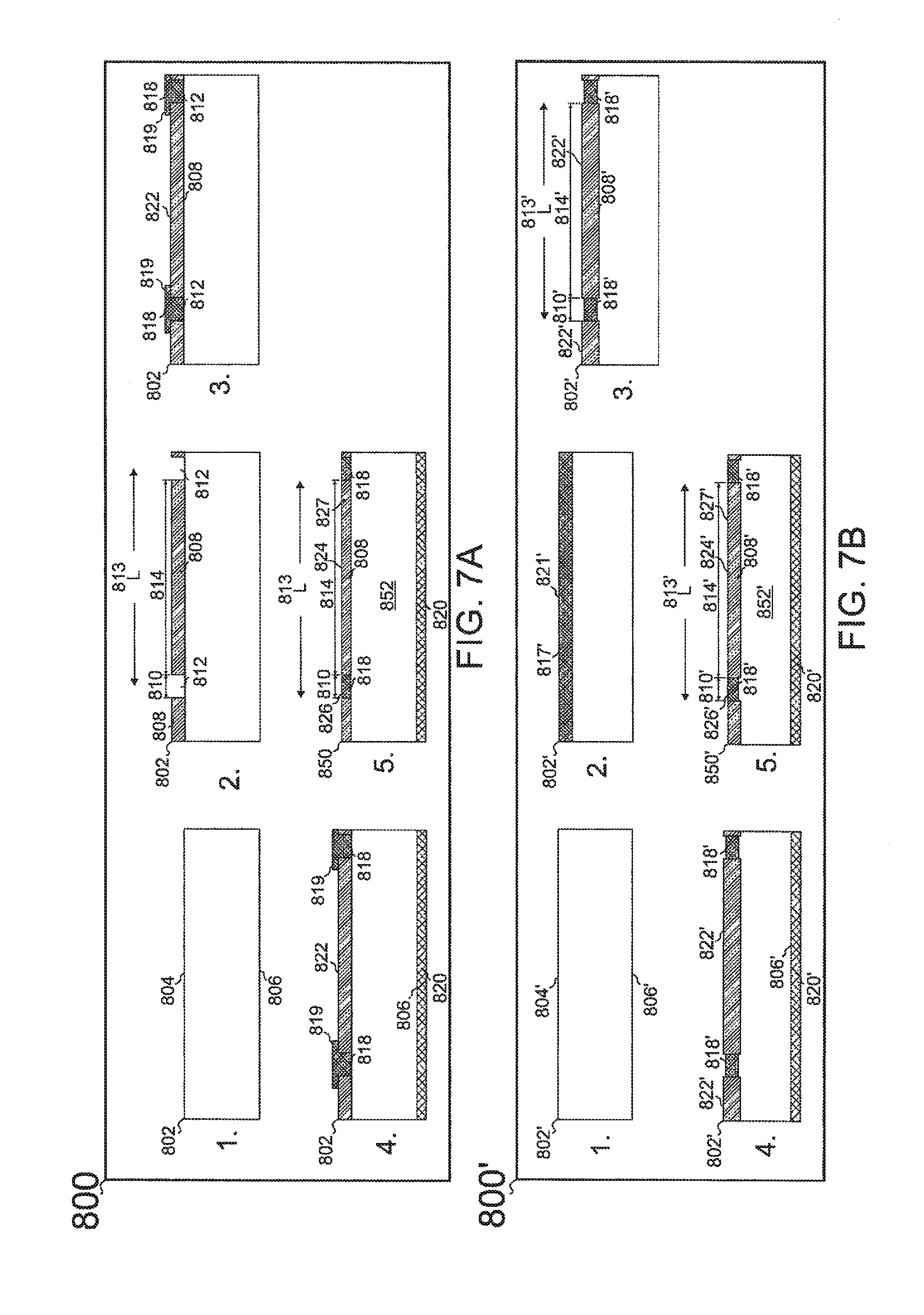
D00013
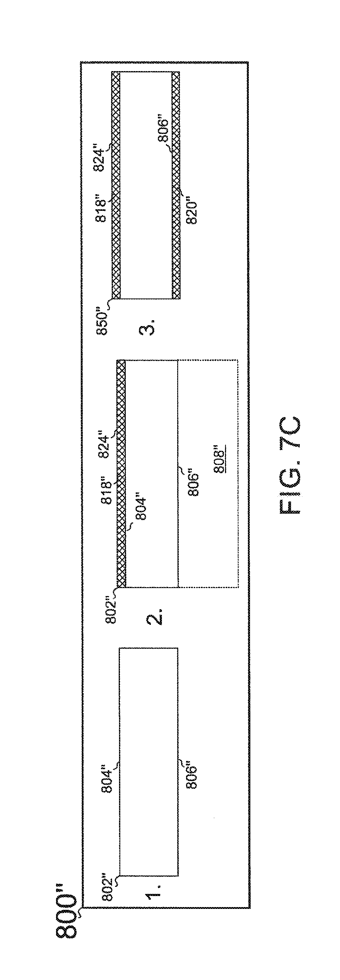
D00014
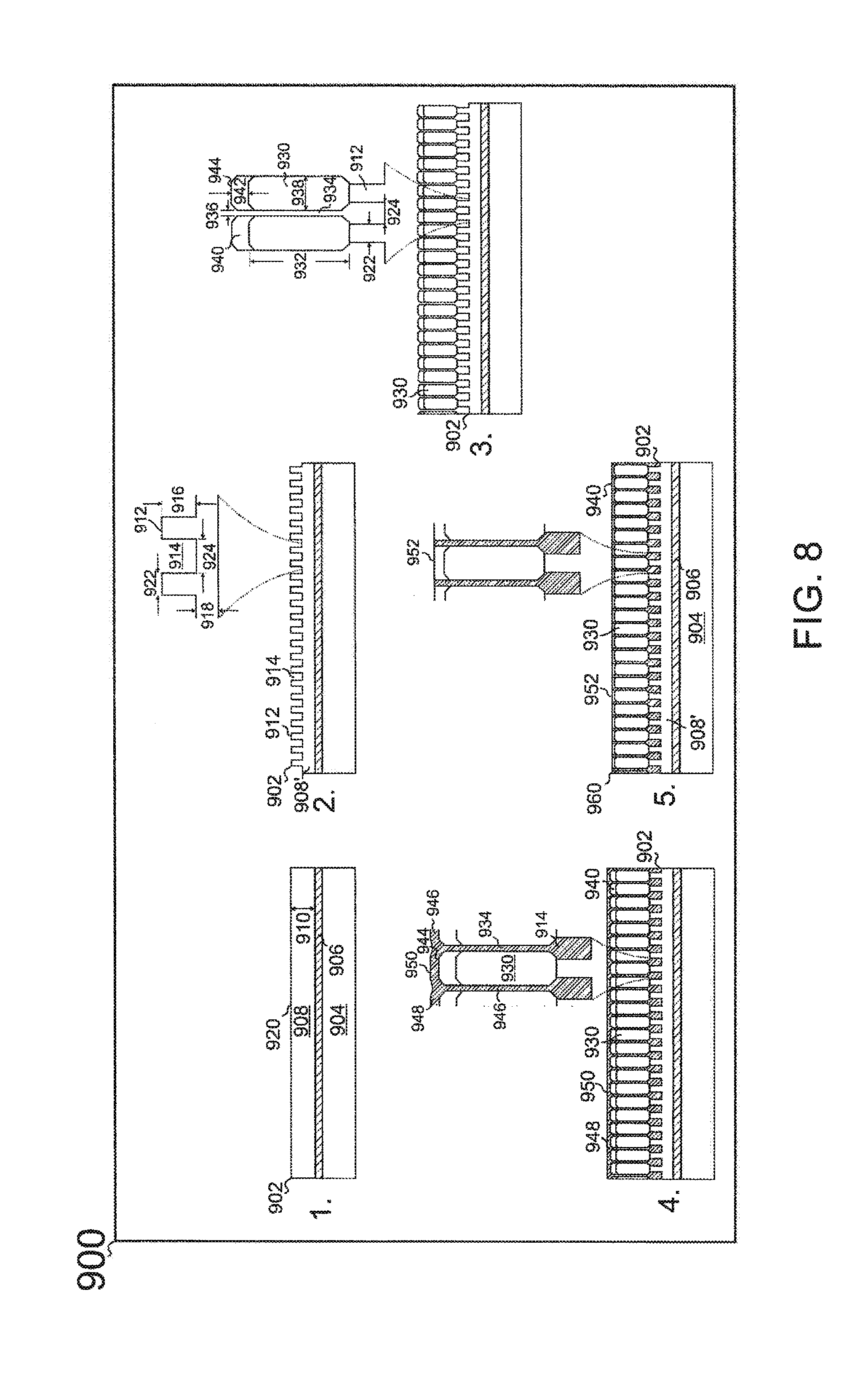
D00015
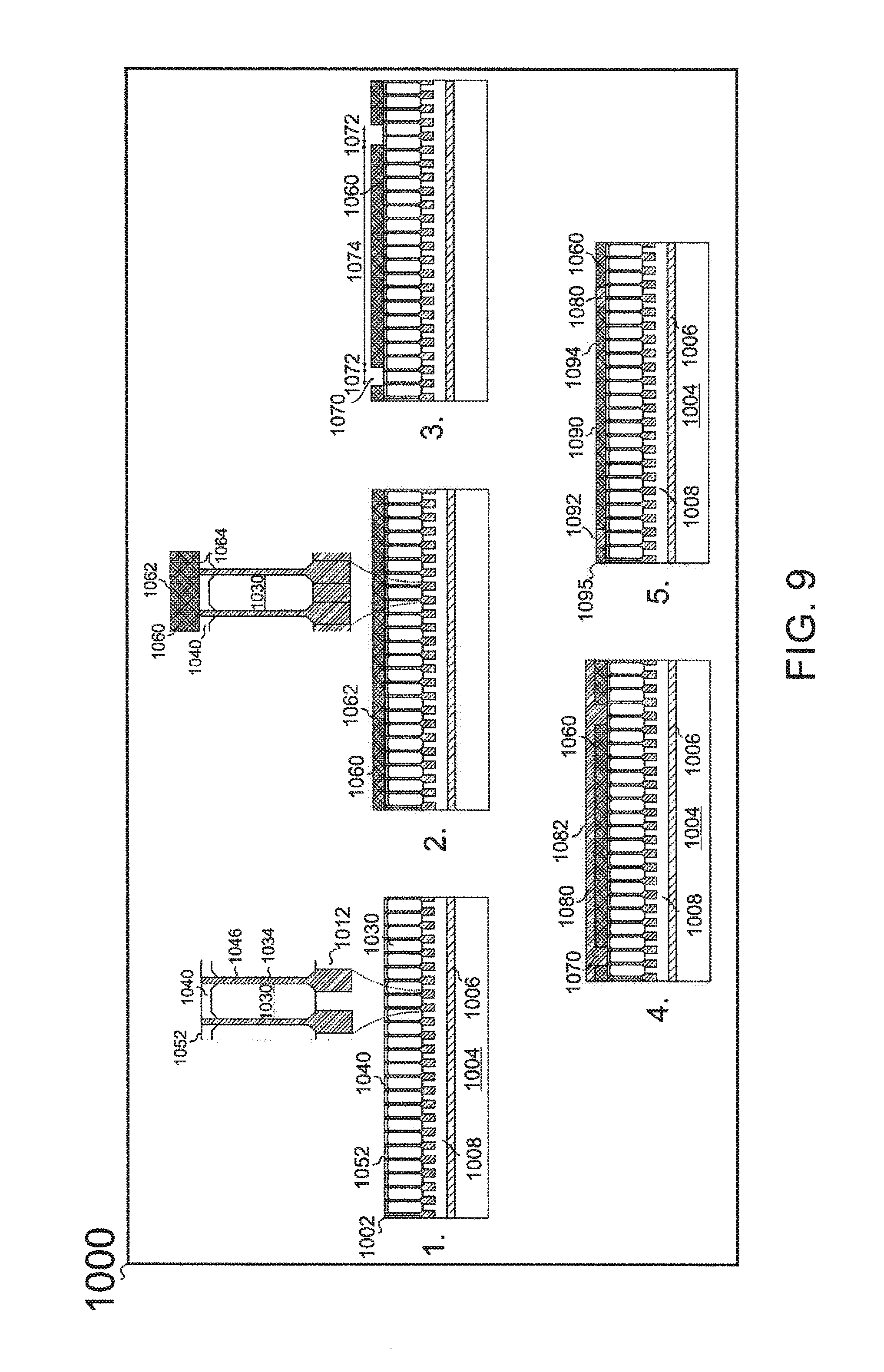
D00016
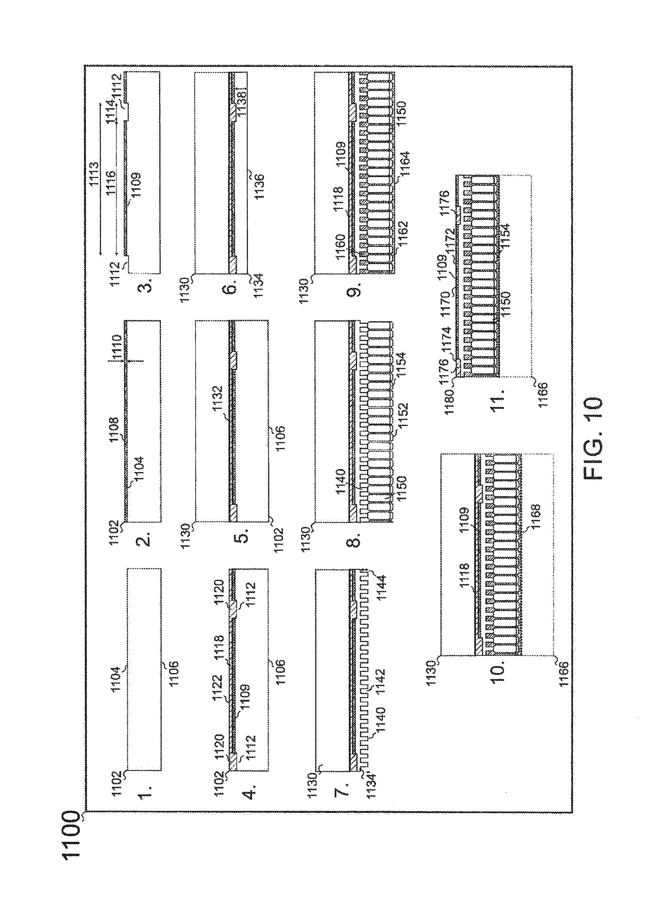
D00017
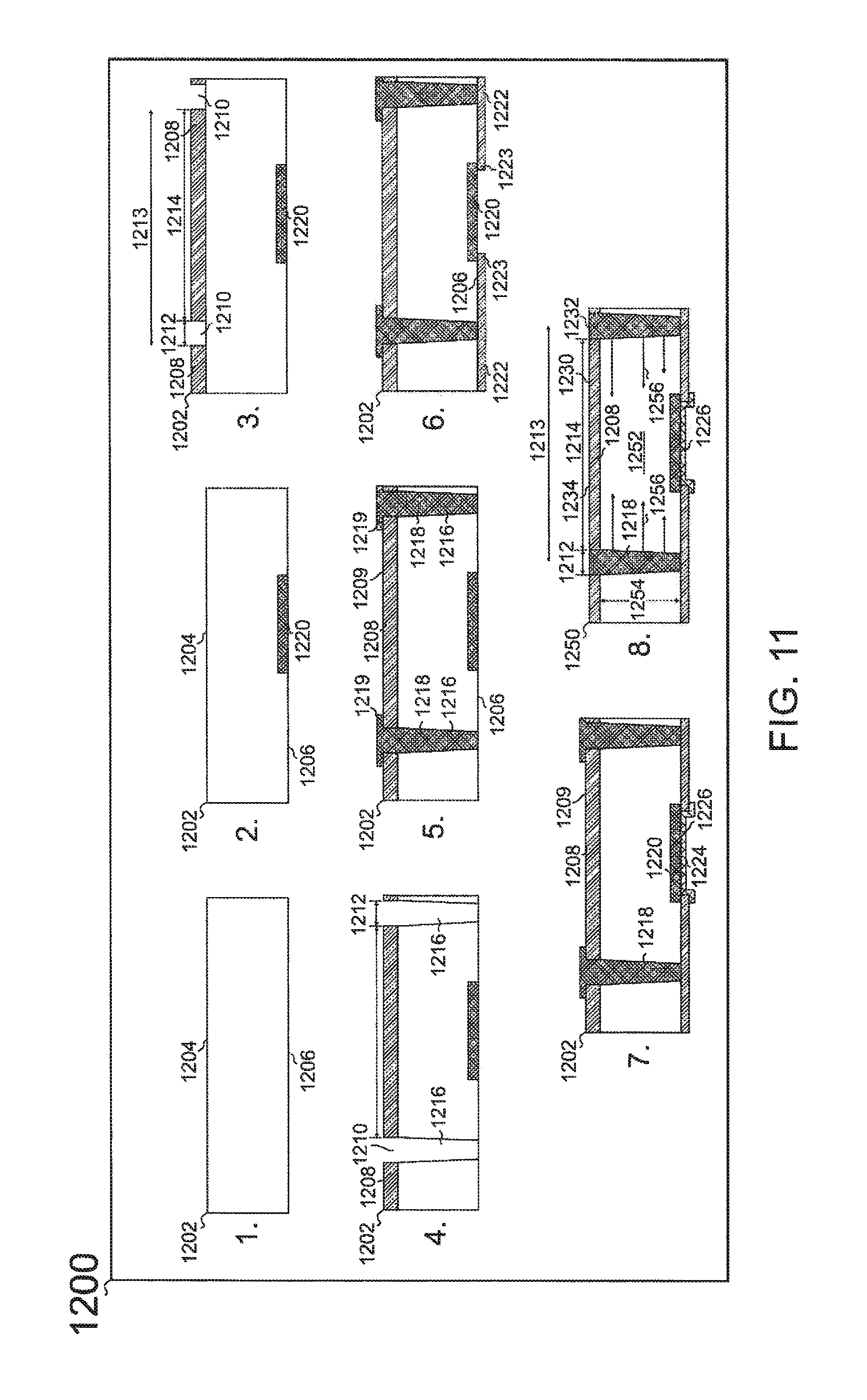
D00018
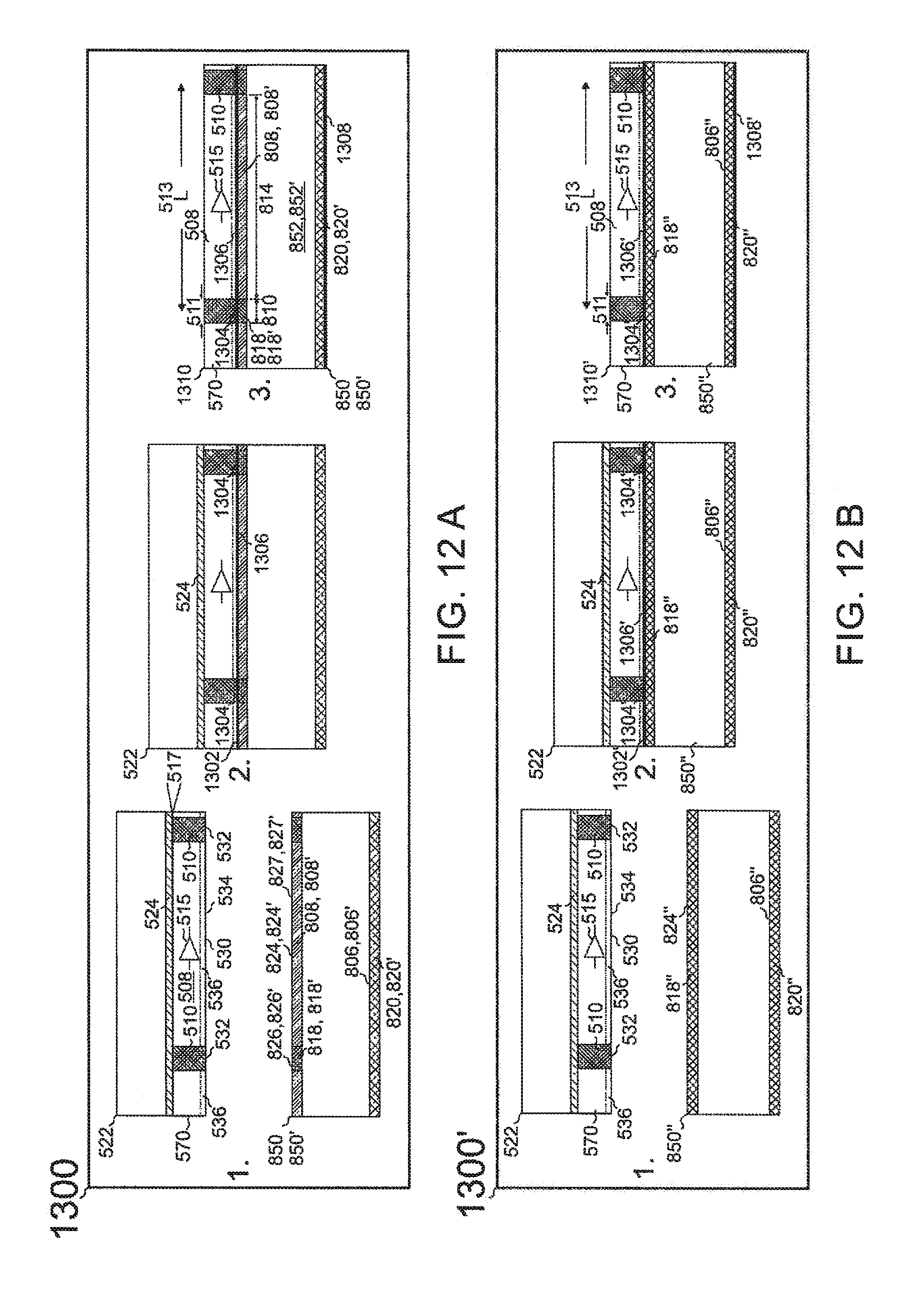
D00019
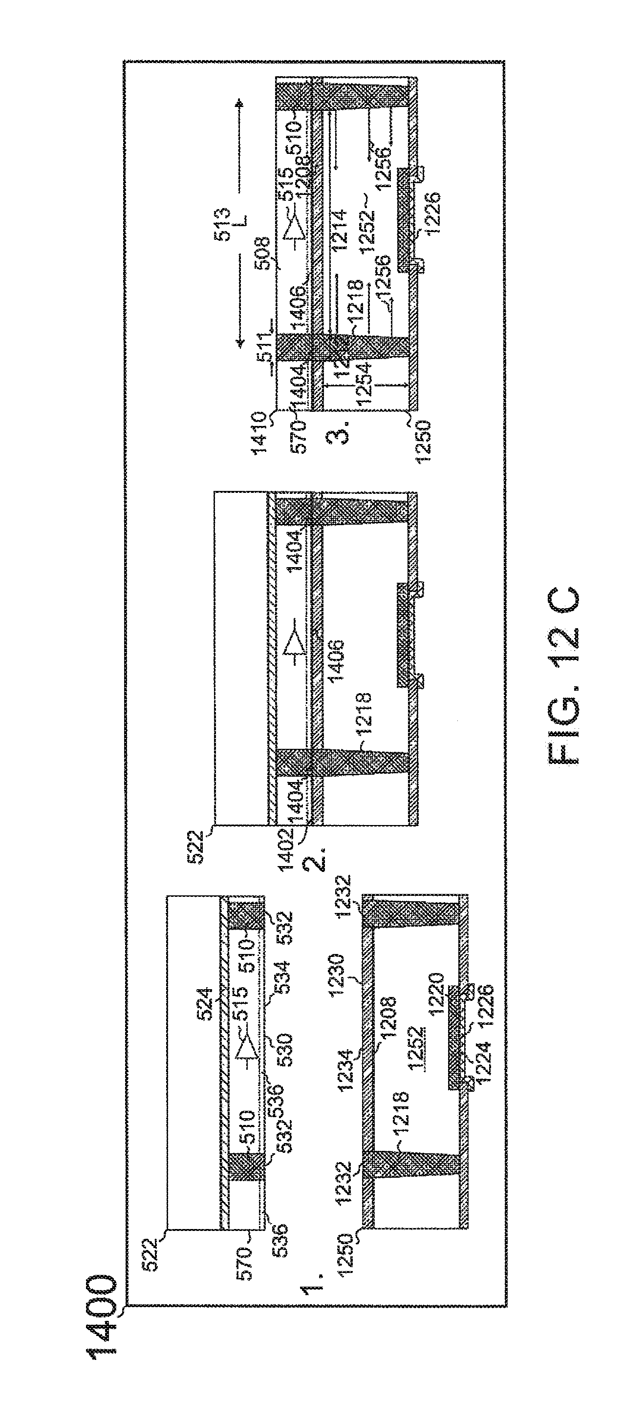
D00020
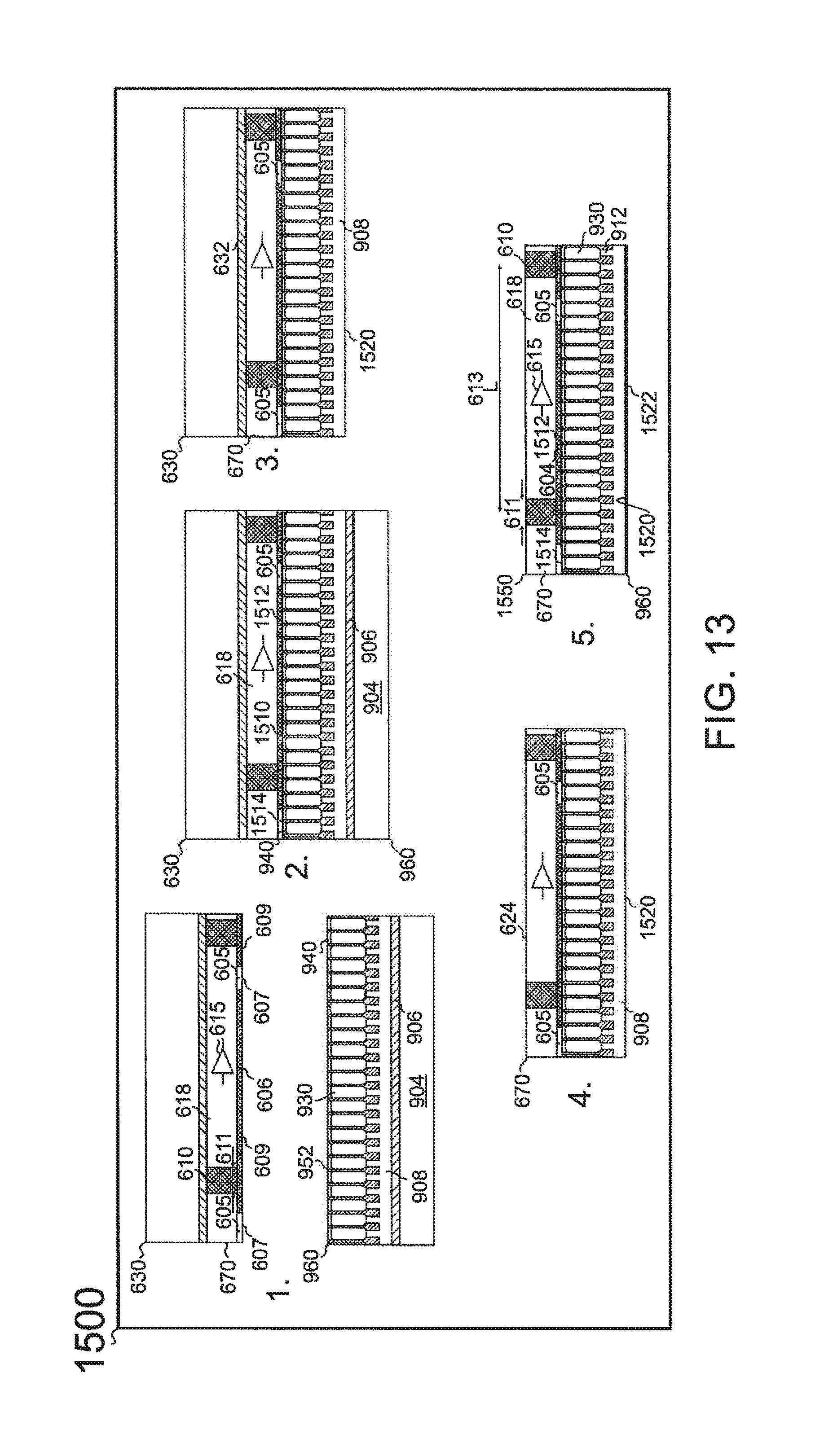
D00021
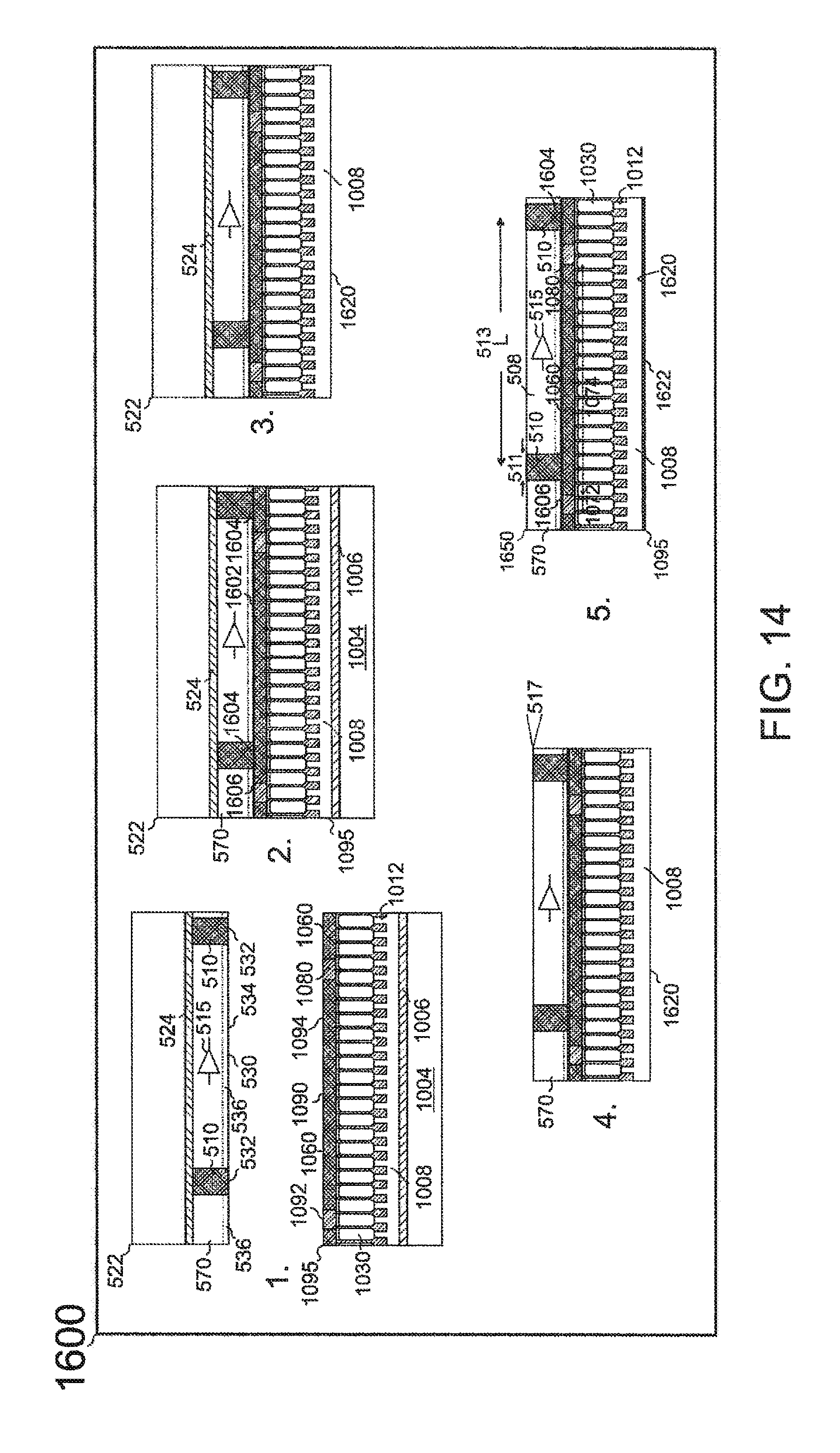
D00022
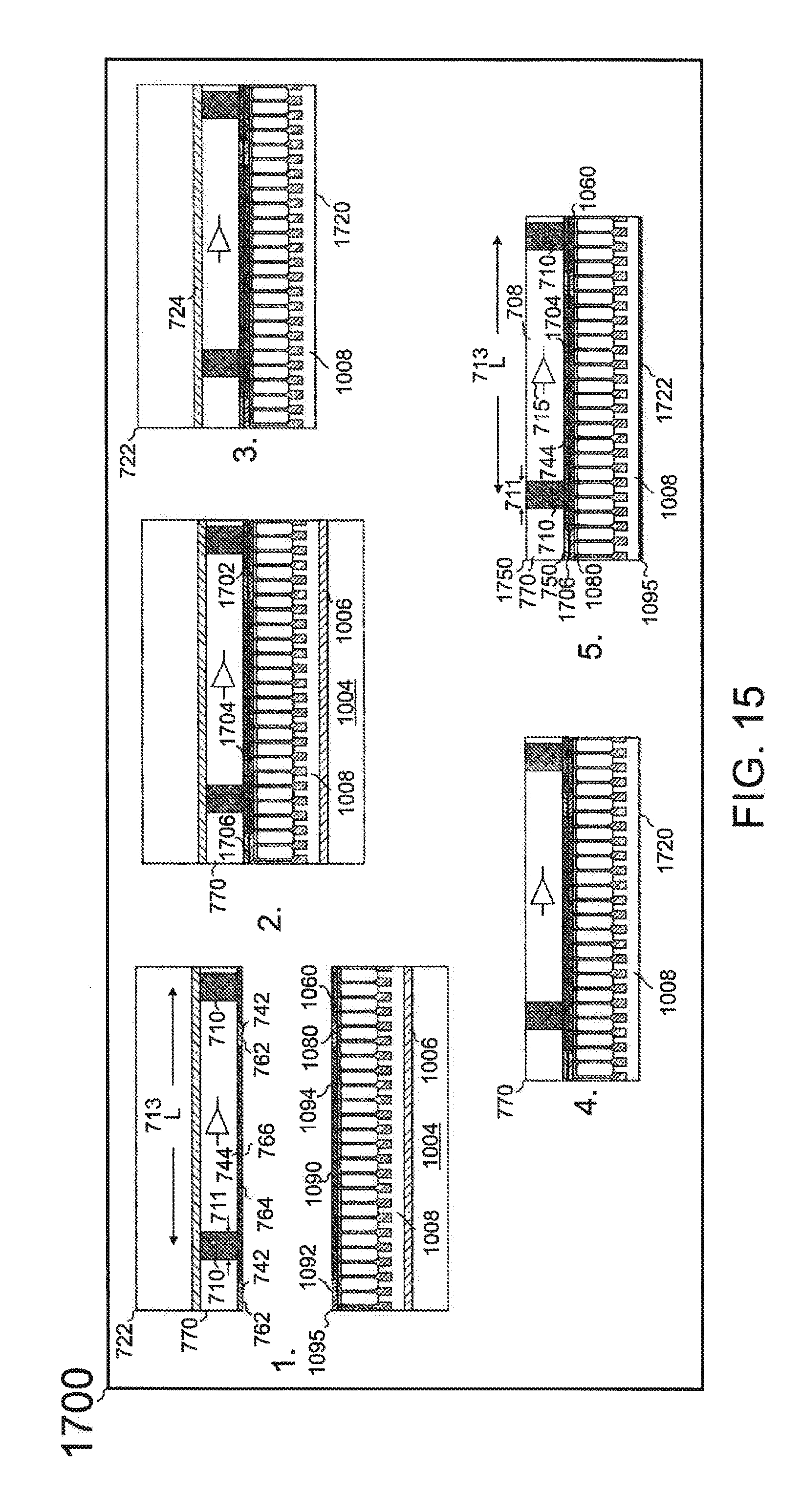
D00023
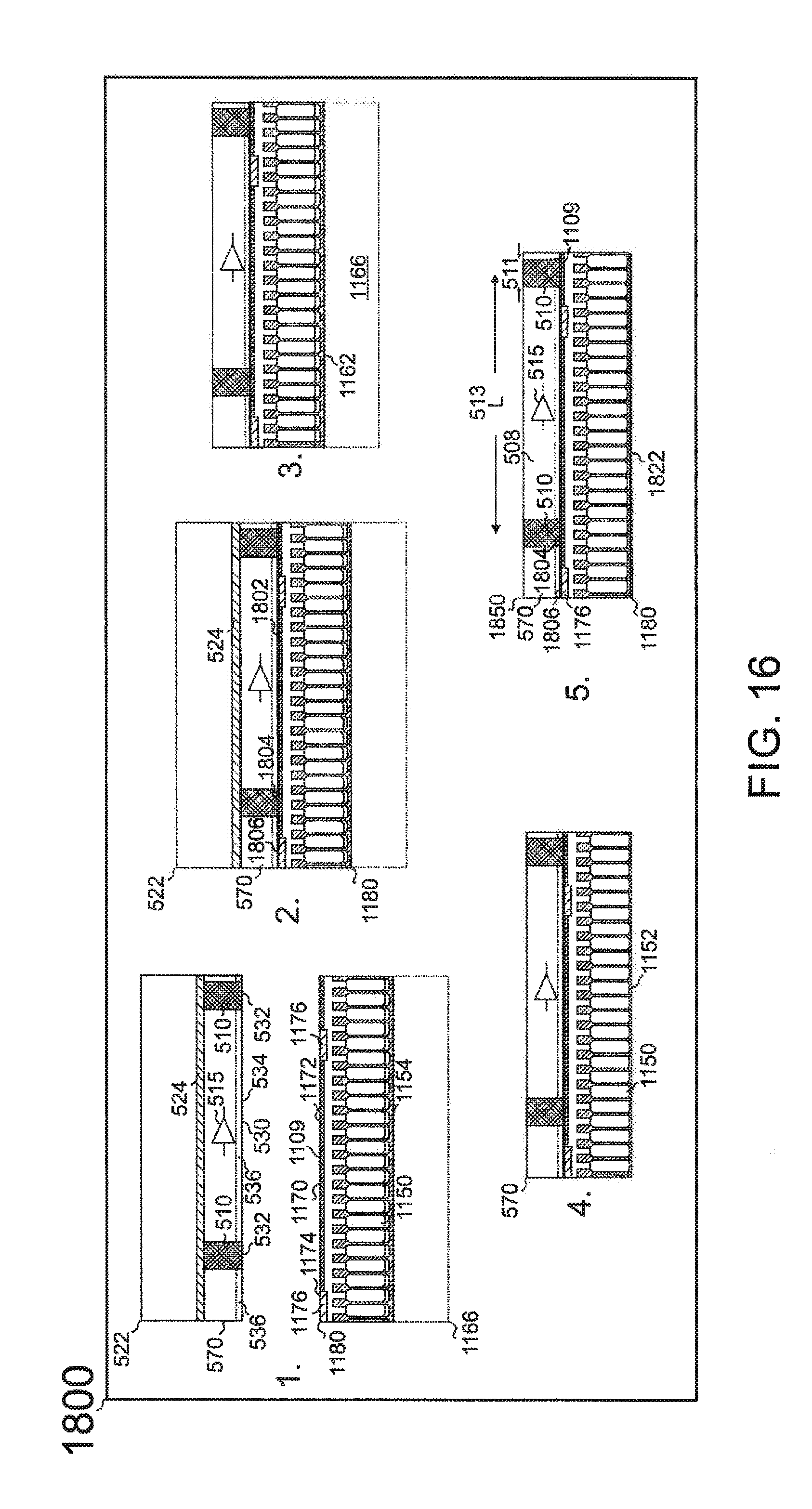
D00024
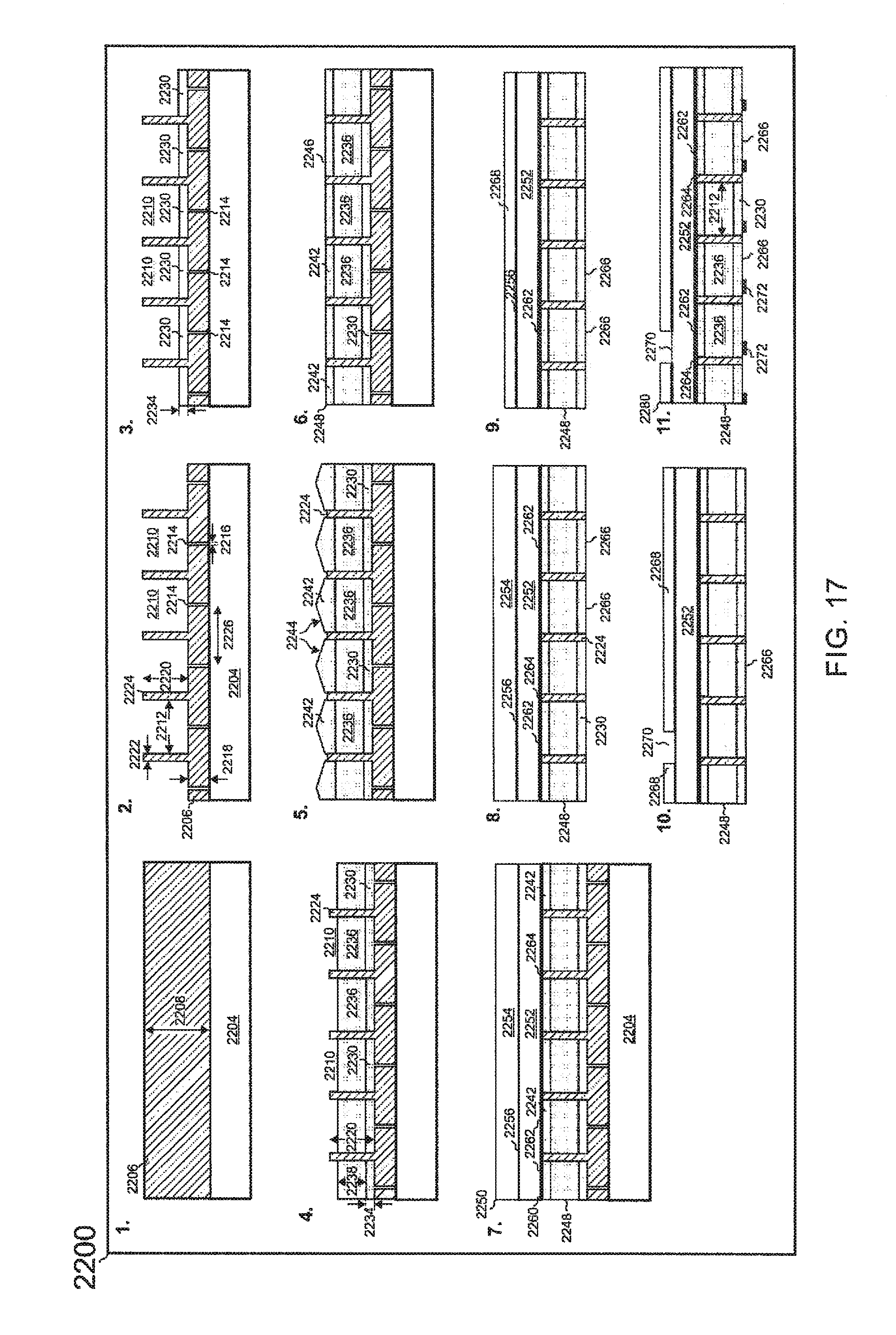
D00025
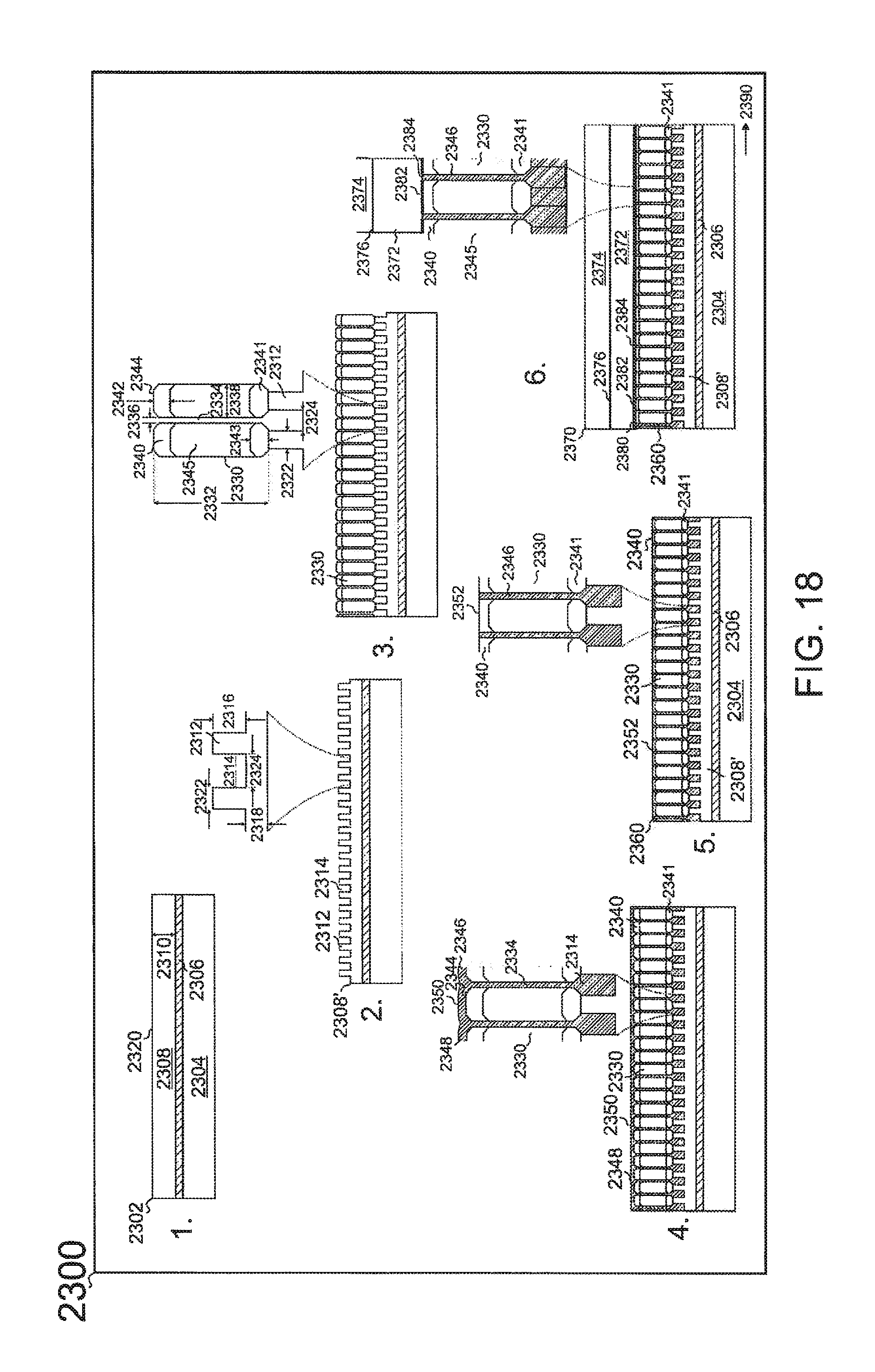
D00026
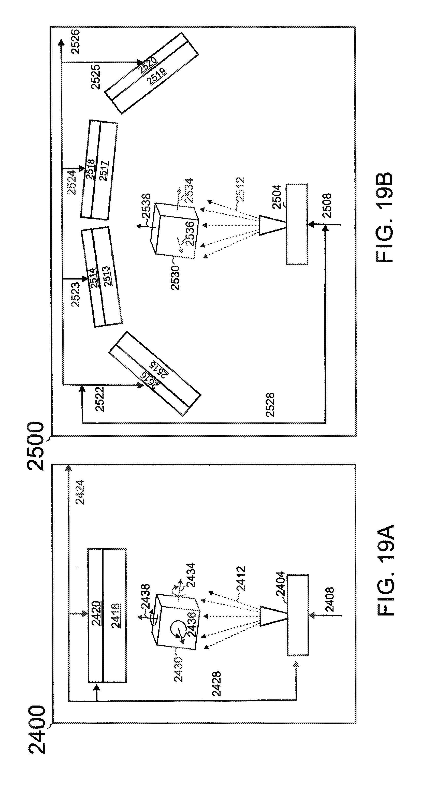
D00027
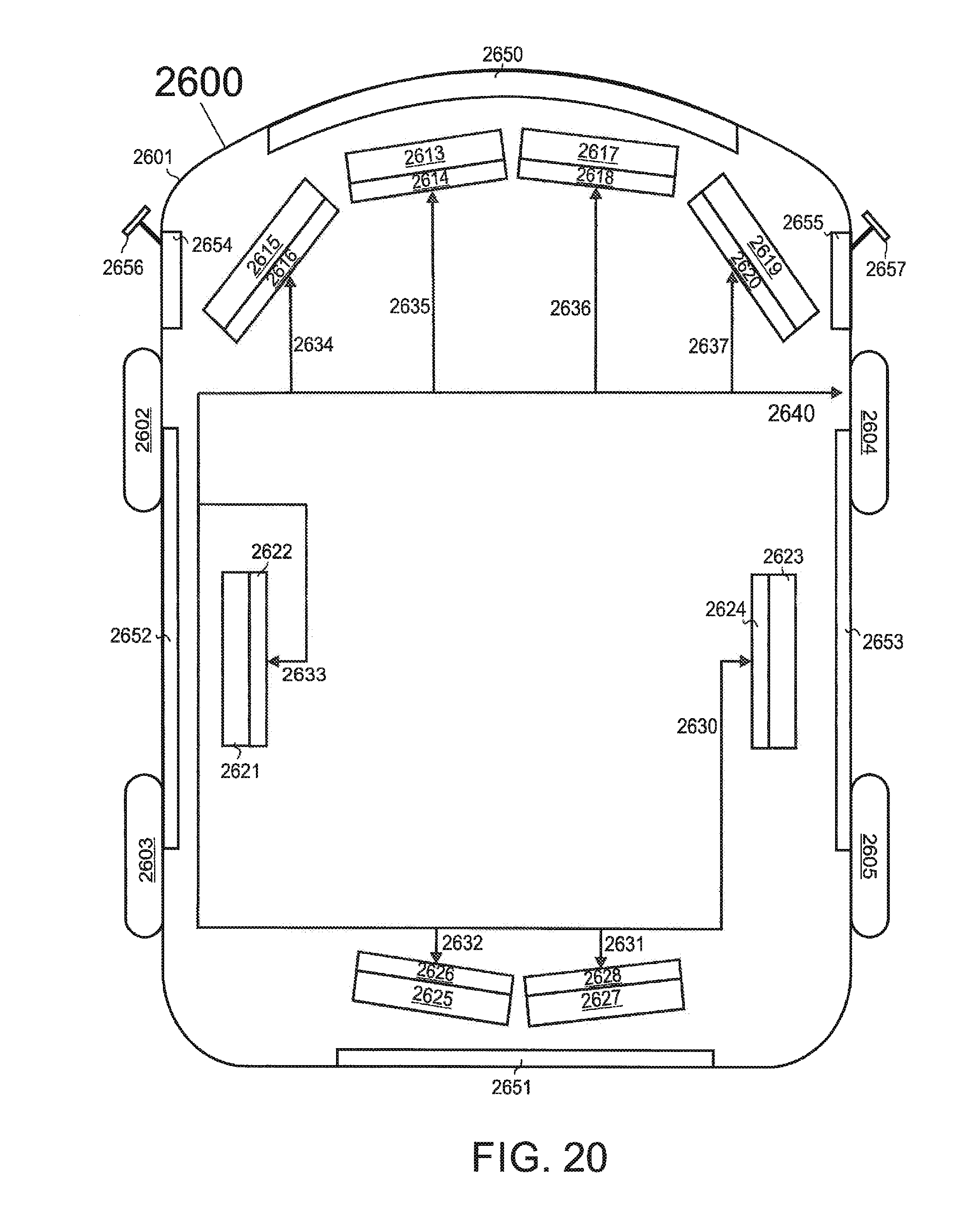
XML
uspto.report is an independent third-party trademark research tool that is not affiliated, endorsed, or sponsored by the United States Patent and Trademark Office (USPTO) or any other governmental organization. The information provided by uspto.report is based on publicly available data at the time of writing and is intended for informational purposes only.
While we strive to provide accurate and up-to-date information, we do not guarantee the accuracy, completeness, reliability, or suitability of the information displayed on this site. The use of this site is at your own risk. Any reliance you place on such information is therefore strictly at your own risk.
All official trademark data, including owner information, should be verified by visiting the official USPTO website at www.uspto.gov. This site is not intended to replace professional legal advice and should not be used as a substitute for consulting with a legal professional who is knowledgeable about trademark law.