Semiconductor Device And Manufacturingmethod Thereof
Ooshima; Kazuhiro
U.S. patent application number 16/119945 was filed with the patent office on 2019-09-19 for semiconductor device and manufacturingmethod thereof. This patent application is currently assigned to Toshiba Memory Corporation. The applicant listed for this patent is Toshiba Memory Corporation. Invention is credited to Kazuhiro Ooshima.
| Application Number | 20190287925 16/119945 |
| Document ID | / |
| Family ID | 67906057 |
| Filed Date | 2019-09-19 |


View All Diagrams
| United States Patent Application | 20190287925 |
| Kind Code | A1 |
| Ooshima; Kazuhiro | September 19, 2019 |
SEMICONDUCTOR DEVICE AND MANUFACTURINGMETHOD THEREOF
Abstract
A semiconductor device includes a semiconductor substrate, at least two first films, a bridge portion, and a conductive member. The two first films are spaced apart from each other, along a first direction which is an in-plane direction of the semiconductor substrate, and along a second direction which is in the in-plane direction of the semiconductor substrate and is perpendicular to the first direction. The bridge portion connects portions of side facing surfaces of the two first films to each other, and has a flat bottom surface. The conductive member is provided under the bottom surface of the bridge portion.
| Inventors: | Ooshima; Kazuhiro; (Kuwana Mie, JP) | ||||||||||
| Applicant: |
|
||||||||||
|---|---|---|---|---|---|---|---|---|---|---|---|
| Assignee: | Toshiba Memory Corporation Tokyo JP |
||||||||||
| Family ID: | 67906057 | ||||||||||
| Appl. No.: | 16/119945 | ||||||||||
| Filed: | August 31, 2018 |
| Current U.S. Class: | 1/1 |
| Current CPC Class: | H01L 21/76877 20130101; H01L 27/11582 20130101; H01L 23/5329 20130101; H01L 27/11565 20130101; H01L 27/11548 20130101; H01L 23/53257 20130101; H01L 27/11556 20130101; H01L 23/528 20130101; H01L 23/5226 20130101; H01L 21/76831 20130101; H01L 2221/1063 20130101; H01L 21/76802 20130101; H01L 23/562 20130101 |
| International Class: | H01L 23/00 20060101 H01L023/00; H01L 23/522 20060101 H01L023/522; H01L 23/528 20060101 H01L023/528; H01L 23/532 20060101 H01L023/532; H01L 21/768 20060101 H01L021/768 |
Foreign Application Data
| Date | Code | Application Number |
|---|---|---|
| Mar 19, 2018 | JP | 2018-050578 |
Claims
1. A semiconductor device comprising: a semiconductor substrate; at least two first films spaced apart from each other along a first direction which is an in-plane direction of the semiconductor substrate, and along a second direction which is in the in-plane direction of the semiconductor substrate and is perpendicular to the first direction; a bridge portion connecting portions of opposed side surfaces of the two first films to each other, the bridge portion having a flat bottom surface; and a conductor provided under the bottom surface of the bridge portion.
2. The semiconductor device according to claim 1, wherein the two first films are stacked films constructed by alternately stacking a conductive layer made of a same material as the conductor, and an insulating layer.
3. The semiconductor device according to claim 2, wherein the bottom surface of the bridge portion is located on the conductive layer as an uppermost layer.
4. The semiconductor device according to claim 2, wherein the conductive layer contains tungsten.
5. The semiconductor device according to claim 1, wherein the bridge portion is formed at a top surface portion of each of the at least two first films.
6. The semiconductor device according to claim 1, wherein the bridge portion is a silicon monoxide film.
7. The semiconductor device according to claim 1, wherein at least one of the two first films is a single-layer film.
8. The semiconductor device according to claim 2, wherein the conductive layer and the insulating layer are alternately stacked on the substrate.
9. The semiconductor device according to claim 1, wherein the conductor is disposed in a space between the at least two first films.
10. A method of manufacturing a semiconductor device, the method comprising: forming a processing target film on a substrate; dividing the processing target film by a groove; filling the groove with a sacrificial film; forming, on the sacrificial film, a mask patterned sous to partially expose the sacrificial film; etching the sacrificial film to a predetermined depth using the mask; burying a bridge portion at a location where the sacrificial film is etched; removing the sacrificial film; and filling a location where the sacrificial film is removed with a conductor.
11. The method according to claim 10, further comprising alternately stacking a first insulating layer and a second insulating layer to form stacked films, the stacked films forming the processing target film.
12. The method according to claim 11, further comprising: replacing the second insulating layer with a conductive layer made of a same material as the conductor.
13. The method according claim 11, wherein the predetermined depth is set to be equal to or less than a distance from an uppermost surface of the stacked films to a top surface of the second insulating layer as an uppermost layer.
14. The method according to claim 11, further comprising: forming, as the sacrificial film, a first sacrificial film that covers a surface of the stacked films and is made of a same material as the second insulating layer, and a second sacrificial film filled in the groove; removing the second sacrificial film; and removing the first sacrificial film and the second insulating layer simultaneously.
15. The method according to claim 12, wherein the conductive layer contains tungsten.
16. The method according to claim 14, wherein the first sacrificial film and the second sacrificial film are formed of different materials.
17. The method according to claim 11, wherein the conductive layer and the insulating layer are alternately stacked on the substrate.
18. The method according to claim 11, wherein the conductor is disposed in a space between stacked films which are separated from each other.
19. The method according to claim 14, further comprising burying the bridge portion in a location where the first sacrificial film and the second sacrificial film are etched.
20. The method according to claim 10, wherein the bridge portion is a silicon monoxide film,
Description
CROSS-REFERENCE TO RELATED APPLICATION
[0001] This application is based upon and claims the benefit of priority from Japanese Patent Application No. 2018-050578, filed Mar. 19, 2018, the entire contents of which are incorporated herein by reference.
FIELD
[0002] Embodiments described herein relate generally to a semiconductor device and a manufacturing method thereof.
BACKGROUND
[0003] In a manufacturing process of a semiconductor device, for example, elongated films may be formed by dividing a film provided on a substrate by a groove. In this case, when the divided film is thick, warpage of the substrate tends to occur. Therefore, there has been proposed a technique of connecting films to each other by a bridge portion.
DESCRIPTION OF THE DRAWINGS
[0004] FIG. 1 is a plan view of a semiconductor device according to some embodiments.
[0005] FIGS. 2A and 2B are sectional views taken along a section line A-A and a section line B-B, respectively.
[0006] FIG. 3 is a sectional view illustrating a process of forming stacked films.
[0007] FIG. 4 is a sectional view illustrating a process of forming a groove.
[0008] FIG. 5 is a sectional view illustrating a process of forming a first sacrificial film.
[0009] FIG. 6 is a sectional view illustrating a process of forming a second sacrificial film.
[0010] FIGS. 7A and 7B are sectional views illustrating a process of forming a resist film.
[0011] FIGS. 8A and 88 are sectional views illustrating a process of etching the sacrificial films.
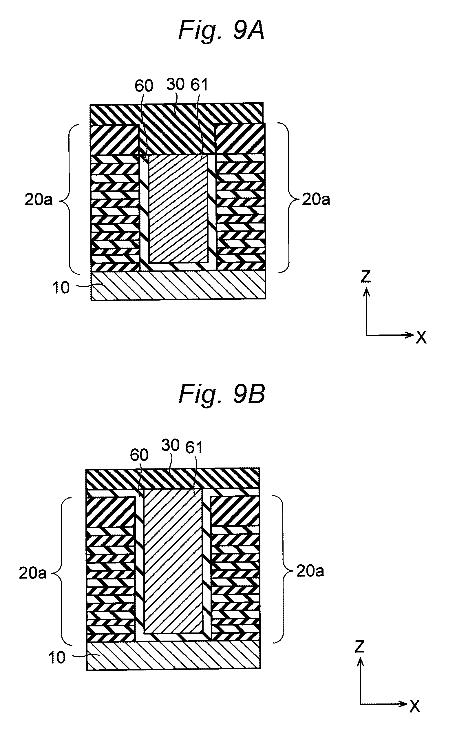
[0012] FIGS. 9A and 98 are sectional views illustrating a process of forming a bridge portion.
[0013] FIGS. 10A and 108 are sectional views illustrating a process of polishing the bridge portion.
[0014] FIGS. 11A and 118 are sectional views illustrating a process of etching the second sacrificial film.
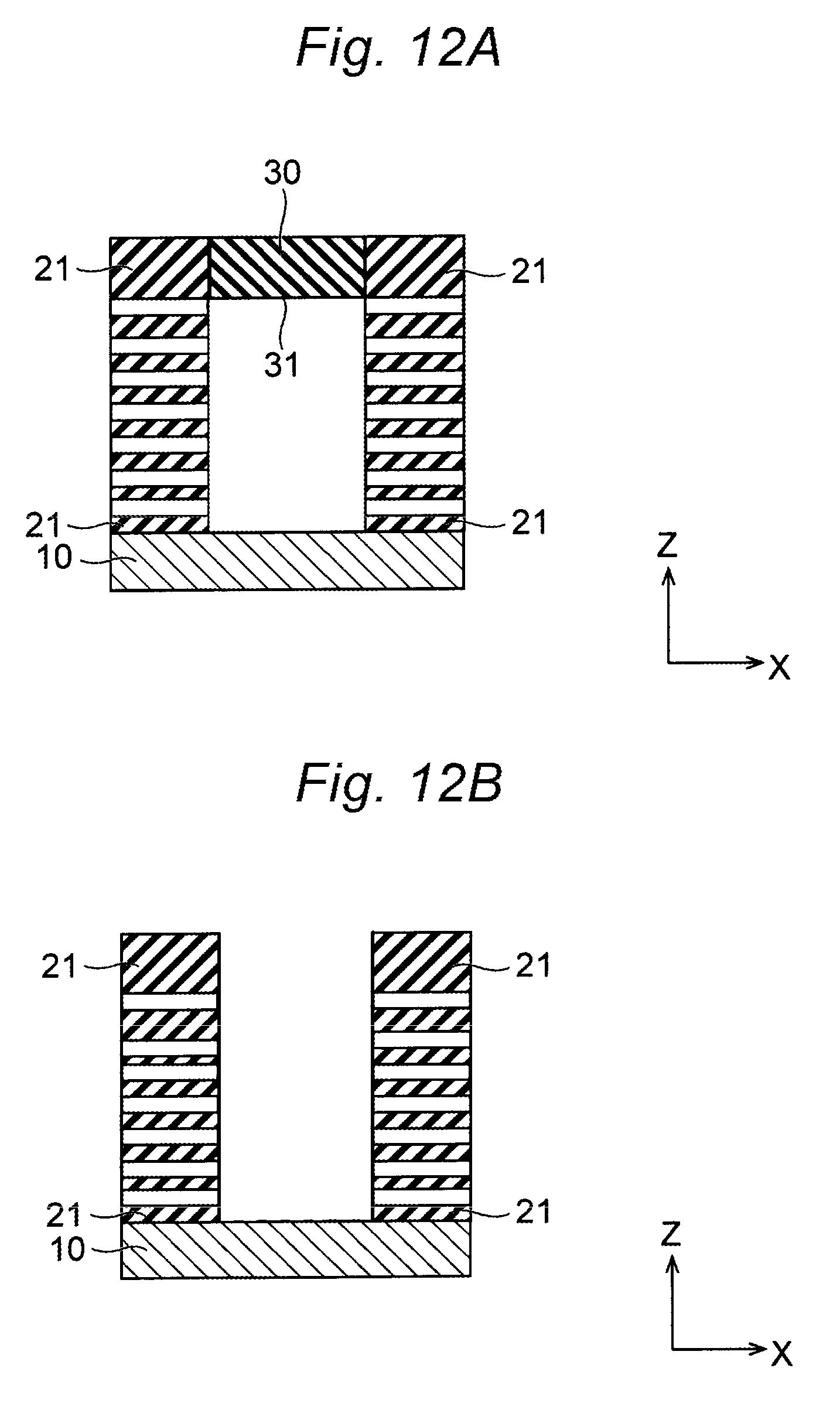
[0015] FIGS. 12A and 128 are sectional views illustrating a process of etching the first sacrificial film and an insulating layer.
[0016] FIGS. 13A and 138 are sectional views illustrating a process of replacing the insulating layer with a conductive layer.
[0017] FIG. 14 is a sectional view illustrating the structure of a bridge portion according to a comparative example.
DETAILED DESCRIPTION
[0018] In the afore-described structures, a bridge portion may be provided, as mentioned above. Coverage of the bridge portion may affect subsequent processing. Embodiments disclosed herein provide a semiconductor device and a manufacturing method thereof in which the coverage of a bridge portion can be improved while the warpage of a substrate can be reduced.
[0019] In general, according to some embodiments, a semiconductor device includes a semiconductor substrate, at least two first films, a bridge portion, and a conductive member. The two first films are spaced apart from each other, along a first direction which is an in-plane direction of the semiconductor substrate, and along a second direction which is in the in-plane direction of the semiconductor substrate and is perpendicular to the first direction. The bridge portion connects portions of opposed side surfaces of the two first films to each other, and has a planar, flat bottom surface. The conductive member is provided under the bottom surface of the bridge portion.
[0020] Hereinafter, certain embodiments will be described with reference to drawings. The embodiments do not limit the present disclosure.
[0021] FIG. 1 is a plan view of a semiconductor device according to an exemplary embodiment. FIG. 2A is a sectional view taken along a section line A-A illustrated in FIG. 1. FIG. 2B is a sectional view taken along a section line B-B illustrated in FIG. 1. The semiconductor device 1 according to the exemplary embodiment is a semiconductor storage device having a three-dimensional structure in which memory cells are stacked.
[0022] As illustrated in FIG. 1, FIG. 2A, and FIG. 2B, the semiconductor device 1 includes a substrate 10, a plurality of stacked films 20, a bridge portion 30, and a conductive member (a conductor) 40. The substrate 10 is a semiconductor substrate containing silicon or the like.
[0023] The plurality of stacked films 20 are spaced apart from each other, as illustrated in FIG. 1, along the X direction (the first direction) which is the in-plane direction of the substrate 10, and along the Y direction (the second direction) which is in the in-plane direction of the substrate 10 and perpendicular to the X direction. Each stacked film 20 includes insulating layers 21 and conductive layers 22. The insulating layers 21 and the conductive layers 22 are alternately stacked in the Z direction perpendicular to the X direction. The insulating layers 21 are silicon oxide (SiO.sub.2) layers. The conductive layers 22 are metal layers containing, for example, tungsten (W).
[0024] A plurality of memory holes 23 are formed in the stacked films 20 (see FIG. 1). The memory holes 23 pass through the stacked films 20. A memory cell (not illustrated) is formed within each memory hole 23 to be electrically connected to the conductive layers 22. The stacked films 20 may be referred to as a first film. An insulating film or a conductive film may be formed between the substrate 10 and the stacked films 20.
[0025] The bridge portion 30 connects portions of side surfaces of the stacked films 20, which are opposed to each other in the X direction, to each other. The bridge portion 30 may reduce the warpage of the substrate 10. The bridge portion 30 has a flat bottom surface 31. In some embodiments, the bottom surface 31 is located on the uppermost conductive layer 22.
[0026] The conductive member 40 is filled in a space present between the stacked films 20. The conductive member 40 is, for example, made of the same material as the conductive layer 22.
[0027] Hereinafter, a method of manufacturing the semiconductor device 1 according to some embodiments will be described. FIGS. 3 to 6 are sectional views corresponding to FIG. 2A. FIGS. 7A, 8A, 9A, 10A, 11A, 12A, and 13A are sectional views corresponding to FIG. 2A, and FIGS. 7B, 8B, 9B, 10B, 11B, 12B, and 13B are sectional views corresponding to FIG. 2B.
[0028] First, as illustrated in FIG. 3, stacked films 20a are formed by alternately stacking the insulating layers 21 and an insulating layer 22a on the substrate 10. The insulating layer 22a is formed as, for example, a silicon nitride (SiN) layer. The stacked films 20a, the insulating layer 21, and the insulating layer 22a may be referred to as processing target films, a first insulating layer, and a second insulating layer, respectively.
[0029] Next, as illustrated in FIG. 4, a groove 50 is formed to divide the stacked films 20a. The groove 50 is formed using, for example, a lithography technique and reactive ion etching (RIE).
[0030] Next, as illustrated in FIG. 5, a first sacrificial film 60 is formed on the surfaces of the stacked films 20a and the bottom surface of the groove 50. The first sacrificial film 60 is made of, for example, the same material as the insulating layer 22a, such as silicon nitride.
[0031] Next, as illustrated in FIG. 6, a second sacrificial film 61 is filled in the groove 50. The second sacrificial film 61 is formed as, for example, a polysilicon film.
[0032] As illustrated in FIGS. 7A and 7B, a resist film 70 (as may also be referred to as a mask) is formed. The resist film 70 is formed as, for example, an organic film. The resist film 70 is, as illustrated in FIG. 7A, patterned so that the first sacrificial film 60 and the second sacrificial film 61 are exposed at a location where the bridge portion 30 is formed.
[0033] Next, as illustrated in FIGS. 8A and 8B, the first sacrificial film 60 and the second sacrificial film 61 are etched using the resist film 70 as a mask. In this process, the etching depth Hi may be equal to or less than, for example, a distance D1 from the uppermost surface of the stacked films 20a to the top surface of the uppermost insulating layer 22a.
[0034] Next, as illustrated in FIG. 9A, the bridge portion 30 is buried in a location where the first sacrificial film 60 and the second sacrificial film 61 are etched. Here, as illustrated in FIG. 9E, the bridge portion 30 is also formed on the top surfaces of the stacked films 20a. The bridge portion 30 is formed as, for example, a silicon monoxide (SiO) or silicon oxide (SiO.sub.2) film. As a result, the stacked films 20a are connected to each other by the bridge portion 30.
[0035] Next, as illustrated in FIGS. 10A and 10B, for example, the bridge portion 30 is flattened by chemical mechanical polishing (CMP) Accordingly, the bridge portion 30 formed on the top surfaces of the stacked films 20a is removed.
[0036] Next, as illustrated in FIGS. 11A and 11B, the second sacrificial film 61 is selectively etched. Here, for example, phosphoric acid at a high temperature is used as an etching solution. Here, the second sacrificial film 61 is removed by isotropic etching, and thus, the bottom surface 31 of the bridge portion 30 is flattened.
[0037] Next, as illustrated in FIGS. 12A and 12B, the first sacrificial film 60 and the insulating layers 22a are simultaneously removed. The first sacrificial film 60 and the insulating layers 22a are made of the same material, and thus may be simultaneously removed.
[0038] Next, as illustrated in FIGS. 13A and 13B, the insulating layers 22a is replaced with the conductive layers 22. Accordingly, the stacked films 20 are completed. Finally, referring back to FIGS. 2A and 2B, the conductive member 40 is buried.
[0039] FIG. 14 is a view illustrating the structure of a bridge portion according to a comparative example. The film of a bridge portion 130 illustrated in FIG. 14 is formed by growing or being deposited from opposed side surfaces of the groove 50. Thus, as illustrated in FIG. 14, the bottom surface of the bridge portion 130 is likely to have an uneven shape with a small contact angle. Therefore, for example, in a process after the bridge portion 130 is formed, foreign matter 100 is likely to adhere to the uneven-shaped portion.
[0040] Meanwhile, in some embodiments, the first sacrificial film 60 and the second sacrificial film 61 are formed under the bridge portion 30 in advance, and the respective sacrificial films are removed after the bridge portion 30 is formed. Therefore, the bottom surface 31 of the bridge portion 30 is flattened, and thus the adherence of the foreign matter 100 is avoided or lessened. In this manner, the coverage of the bridge portion 30 may be improved, so that the space under the bridge portion 30 may be utilized as a wiring composed of the conductive member 40. With respect to the flatness of the bottom surface 31, after the insulating layers 22a are replaced with the conductive layers 22, an unevenness which is less than a minimum contact angle of a solution for etching back a film forming material may be tolerated.
[0041] In some embodiments, the etching amounts of the first sacrificial film 60 and the second sacrificial film 61 may be adjusted to control the depth of the bridge portion 30. Thus, according to the structure of the stacked films 20, the location of the bottom surface 31 of the bridge portion 30 may be freely controlled. For example, when the bottom surface 31 is located on the uppermost insulating layer 22a as in some embodiments, it is possible to prevent the bridge portion 30 from interfering with the replacement of the insulating layers 22a by the conductive layers 22.
[0042] In some embodiments, a film connected by the bridge portion 30 may be the stacked films 20, but may be a single layer film.
[0043] While certain embodiments have been described, these embodiments have been presented by way of example only, and are not intended to limit the scope of the inventions. Indeed, the novel embodiments described herein may be embodied in a variety of other forms; furthermore, various omissions, substitutions and changes in the form of embodiments described herein may be made without departing from the spirit of the inventions. The accompanying claims and their equivalents are intended to cover such forms or modifications as would fall within the scope and spirit of the inventions.
* * * * *
D00000
D00001
D00002
D00003
D00004
D00005
D00006
D00007
D00008
D00009
D00010
D00011
D00012

XML
uspto.report is an independent third-party trademark research tool that is not affiliated, endorsed, or sponsored by the United States Patent and Trademark Office (USPTO) or any other governmental organization. The information provided by uspto.report is based on publicly available data at the time of writing and is intended for informational purposes only.
While we strive to provide accurate and up-to-date information, we do not guarantee the accuracy, completeness, reliability, or suitability of the information displayed on this site. The use of this site is at your own risk. Any reliance you place on such information is therefore strictly at your own risk.
All official trademark data, including owner information, should be verified by visiting the official USPTO website at www.uspto.gov. This site is not intended to replace professional legal advice and should not be used as a substitute for consulting with a legal professional who is knowledgeable about trademark law.