Reactor, System Including The Reactor, And Methods Of Manufacturing And Using Same
Blomberg; Tom ; et al.
U.S. patent application number 15/923834 was filed with the patent office on 2019-09-19 for reactor, system including the reactor, and methods of manufacturing and using same. The applicant listed for this patent is ASM IP Holding B.V.. Invention is credited to Tom Blomberg, Varun Sharma, Chiyu Zhu.
| Application Number | 20190287769 15/923834 |
| Document ID | / |
| Family ID | 67904533 |
| Filed Date | 2019-09-19 |


| United States Patent Application | 20190287769 |
| Kind Code | A1 |
| Blomberg; Tom ; et al. | September 19, 2019 |
REACTOR, SYSTEM INCLUDING THE REACTOR, AND METHODS OF MANUFACTURING AND USING SAME
Abstract
A reactor for processing substrates and methods for manufacturing and using the reactor are disclosed. Specifically, the reactor can include a material that forms gas compounds. The gas compounds are then easily removed from the reactor, thus reducing or avoiding contamination of the substrates in the reactor that would otherwise arise.
| Inventors: | Blomberg; Tom; (Vantaa, FI) ; Sharma; Varun; (Helsinki, FI) ; Zhu; Chiyu; (Helsinki, FI) | ||||||||||
| Applicant: |
|
||||||||||
|---|---|---|---|---|---|---|---|---|---|---|---|
| Family ID: | 67904533 | ||||||||||
| Appl. No.: | 15/923834 | ||||||||||
| Filed: | March 16, 2018 |
| Current U.S. Class: | 1/1 |
| Current CPC Class: | H01L 21/68757 20130101; H01J 37/32357 20130101; H01J 37/32715 20130101; H01J 37/32504 20130101; H01L 21/67069 20130101; H01J 37/3244 20130101; H01J 2237/3341 20130101 |
| International Class: | H01J 37/32 20060101 H01J037/32; H01L 21/67 20060101 H01L021/67; H01L 21/687 20060101 H01L021/687 |
Claims
1. A semiconductor processing system comprising: a reaction chamber, the reaction chamber comprising a first material; a susceptor, the susceptor comprising a second material and being configured to hold a substrate for processing; a showerhead, the showerhead comprising a third material; and a first gas source, the first gas source providing a first gas precursor to the reaction chamber in a process of etching a film on the substrate, wherein the first material, the second material, and the third material react with one or more of the first gas precursor and a second gas precursor to form a gas compound.
2. The semiconductor processing system of claim 1, wherein the first gas precursor comprises one or more of or is derived from one or more of: TiCl.sub.4, TiF.sub.4, TiCl.sub.x, TiF.sub.x, MoCl.sub.x, MoF.sub.x, WCl.sub.x, WF.sub.x, NbCl.sub.x, NbF.sub.x, TaCl.sub.x, TaF.sub.x, VCl.sub.x, VF.sub.x, AlCl.sub.x, HfCl.sub.x or ZrCl.sub.x.
3. The semiconductor processing system of claim 1, wherein the first material comprises at least one of: tungsten, molybdenum, titanium, niobium, tantalum, vanadium, aluminum, hafnium, zirconium, zinc, vanadium alloy, zinc alloy, quartz, borosilicate quartz, and stainless steel.
4. The semiconductor processing system of claim 1, wherein the second material comprises at least one of: tungsten, molybdenum, titanium, niobium, tantalum, vanadium, aluminum, hafnium, zirconium, zinc, vanadium alloy, zinc alloy, quartz, borosilicate quartz, and stainless steel.
5. The semiconductor processing system of claim 1, wherein the third material comprises at least one of: tungsten, molybdenum, titanium, niobium, tantalum, vanadium, aluminum, hafnium, zirconium, zinc, vanadium alloy, zinc alloy, quartz, borosilicate quartz, and stainless steel.
6. The semiconductor processing system of claim 1, further comprising a reaction chamber lining disposed on an interior wall of the reaction chamber, the reaction chamber lining comprising a fourth material that reacts with one or more of the first gas precursor and the second gas precursor to form a gas compound.
7. The semiconductor processing system of claim 6, wherein the fourth material comprises at least one of: tungsten, molybedenum, titanium, niobium, tantalum, vanadium, aluminum, hafnium, zirconium, zinc, vanadium alloy, zinc alloy, quartz, borosilicate quartz, and stainless steel.
8. The semiconductor processing system of claim 6, wherein the reaction chamber lining has a thickness ranging: between 0.1 mm and 10 mm, between 0.5 and 5 mm, between 1 and 3 mm, between 0.0001 and 0.001 mm, between 0.001 and 0.01 mm, or between 0.01 and 0.1 mm, below 10 mm and greater than 10 nm, greater than 100 nm, greater than 1 .mu.m, greater than 10 .mu.m, or greater than 100 .mu.m.
9. The semiconductor processing system of claim 1, wherein the first gas source provides a gas comprising at least one of: a non-metal halide, an organic halide, and a metaloxyhalide.
10. A method of forming a semiconductor processing reactor, the method comprising: providing a reaction chamber, the reaction chamber comprising a first material; providing a susceptor, the susceptor comprising a second material and being configured to hold a substrate for processing; providing a showerhead, the showerhead comprising a third material; and providing a first gas source, the first gas source providing a first gas precursor to the reaction chamber in a process of etching a film on the substrate, wherein the first material, the second material, and the third material react with one or more of the first gas precursor and a second gas precursor to form a gas compound.
11. The method of claim 10, wherein the first material comprises at least one of: tungsten, molybedenum, titanium, niobium, tantalum, vanadium, aluminum, hafnium, zirconium, zinc, vanadium alloy, zinc alloy, quartz, borosilicate quartz, and stainless steel.
12. The method of claim 10, wherein the second material comprises at least one of: tungsten, molybdenum, titanium, niobium, tantalum, vanadium, aluminum, hafnium, zirconium, zinc, vanadium alloy, zinc alloy, quartz, borosilicate quartz, and stainless steel.
13. The method of claim 10, wherein the third material comprises at least one of: tungsten, molybdenum, titanium, niobium, tantalum, vanadium, aluminum, hafnium, zirconium, zinc, vanadium alloy, zinc alloy, quartz, borosilicate quartz, and stainless steel.
14. The method of claim 10, wherein the first gas precursor comprises one or more of or is derived from one or more of: TiCl.sub.4, TiF.sub.4, TiCl.sub.x, TiF.sub.x, MoCl.sub.x, MoF.sub.x, WCl.sub.x, WF.sub.x, NbCl.sub.x, NbF.sub.x, TaCl.sub.x, TaF.sub.x, VCl.sub.x, VF.sub.x, , AlCl.sub.x, HfCl.sub.x and ZrCl.sub.x.
15. The method of claim 10, further comprising: providing a reaction chamber lining disposed on an interior wall of the reaction chamber, the reaction chamber lining comprising a fourth material that reacts with one or more of the first gas precursor and the second gas precursor to form a gas compound.
16. The method of claim 15, wherein the fourth material comprises at least one of: tungsten, molybdenum, titanium, niobium, tantalum, vanadium, aluminum, hafnium, zirconium, zinc, vanadium alloy, zinc alloy, quartz, borosilicate quartz, and stainless steel.
17. The method of claim 15, wherein the reaction chamber lining has a thickness ranging: between 0.1 mm and 10 mm, between 0.5 and 5 mm, between 1 and 3 mm, between 0.0001 and 0.001 mm, between 0.001 and 0.01 mm, between 0.01 and 0.1 mm, below 10 mm and greater than 10 nm, greater than 100 nm, greater than 1 greater than 10 .mu.m, or greater than 100 .mu.m.
18. The method of claim 10, wherein the first gas source provides a gas comprising at least one of: a non-metal halide, an organic halide, and a metaloxyhalide.
19. A semiconductor processing system comprising: a reaction chamber, the reaction chamber comprising a first material; a susceptor, the susceptor comprising a second material and being configured to hold a substrate for processing; a gas distribution structure in the reaction chamber or coupled to the reaction chamber, the gas distribution structure comprising a third material; and a first gas source, the first gas source providing a first gas precursor to the reaction chamber in a process of etching a film on the substrate, wherein the first material, the second material, and the third material react with one or more of the first gas precursor and a second gas precursor to form a gas compound.
20. The semiconductor processing system of claim 19, wherein the gas distribution structure comprises a showerhead.
21. The semiconductor processing system of claim 19, wherein the reaction chamber is a cross-flow reaction chamber.
Description
FIELD OF INVENTION
[0001] The present disclosure generally relates to gas-phase systems, reactors, and methods. More particularly, the disclosure relates to gas-phase reactors, systems, and methods that can be used in the production of devices, such as semiconductor devices.
BACKGROUND OF THE DISCLOSURE
[0002] Semiconductor device manufacturing can include a dry etching process in a substrate processing reactor. The dry etching process may comprise exposing a substrate to a bombardment of ions generated by reactive gases, for example. The reactive gases may include halide chemistries, such as gases with fluoride or chloride atoms. The dry etching process may utilize remote plasma or direct plasma in order to activate the reactive gases--e.g., to form the ions and/or other reactive species.
[0003] The substrate may have materials that are corrosion resistant, such as transition metal nitrides, transition metal oxides, or transition metal carbides, for example, to be etched during the dry etch process. These corrosion-resistant materials may require strongly reactive etch gases to react with the corrosion-resistant materials. During an etch process, the strongly reactive gases may not only etch materials from the substrate, but may also react with walls of the substrate processing reactor. This may lead to formation of contaminants and deposition of the contaminants onto the substrate being processed. The contamination issue may be increased when the reactors operate at higher temperatures and/or with particular chemistries.
[0004] As a result, a reactor, system, and method that mitigate or reduce contaminants on the substrate are desired.
SUMMARY OF THE DISCLOSURE
[0005] Various embodiments of the present disclosure provide improved systems, reactors, and methods for processing a substrate in a reactor. While the ways in which the various drawbacks of the prior art are discussed in greater detail below, in general, the systems, reactors, and methods can be used to fabricate devices, while mitigating contamination on a surface of a substrate that might otherwise occur.
[0006] In accordance with at least one embodiment of the disclosure, a system (e.g., a semiconductor processing system) includes a reaction chamber comprising a first material; a susceptor comprising a second material and being configured to hold a substrate for processing; a gas distribution structure (e.g., a showerhead) comprising a third material; and a first gas source for providing a first gas precursor to the reaction chamber in a process of etching a film on the substrate, wherein the first material, the second material, and the third material react with one or more of the first gas precursor and a second gas precursor to form a (e.g., volatile) gas compound that can be purged from the reaction chamber.
[0007] In accordance with at least one other embodiment of the disclosure, a method of forming a semiconductor processing device includes the steps of providing a reaction chamber comprising a first material; providing a susceptor comprising a second material and being configured to hold a substrate for processing; providing a gas distribution structure (e.g., a showerhead) comprising a third material; and providing a first gas source providing a first gas precursor to the reaction chamber in a process of etching a film on the substrate, wherein the first material, the second material, and the third material react with one or more of the first gas precursor and a second gas precursor to form a (e.g., volatile) gas compound that can be purged from the reaction chamber.
[0008] For purposes of summarizing the invention and the advantages achieved over the prior art, certain objects and advantages of the invention have been described herein above. Of course, it is to be understood that not necessarily all such objects or advantages may be achieved in accordance with any particular embodiment of the invention. Thus, for example, those skilled in the art will recognize that the invention may be embodied or carried out in a manner that achieves or optimizes one advantage or group of advantages as taught or suggested herein without necessarily achieving other objects or advantages as may be taught or suggested herein.
[0009] All of these embodiments are intended to be within the scope of the invention herein disclosed. These and other embodiments will become readily apparent to those skilled in the art from the following detailed description of certain embodiments having reference to the attached figures, the invention not being limited to any particular embodiment(s) disclosed.
BRIEF DESCRIPTION OF THE DRAWING FIGURES
[0010] These and other features, aspects, and advantages of the invention disclosed herein are described below with reference to the drawings of certain embodiments, which are intended to illustrate and not to limit the invention.
[0011] FIG. 1 illustrates a cross-sectional view of a reactor in accordance with at least one embodiment of the invention.
[0012] FIG. 2 illustrates a cross-sectional view of another reactor in accordance with at least one embodiment of the invention.
[0013] It will be appreciated that elements in the figures are illustrated for simplicity and clarity and have not necessarily been drawn to scale. For example, the dimensions of some of the elements in the figures may be exaggerated relative to other elements to help improve understanding of illustrated embodiments of the present disclosure.
DETAILED DESCRIPTION OF EXEMPLARY EMBODIMENTS
[0014] Although certain embodiments and examples are disclosed below, it will be understood by those in the art that the invention extends beyond the specifically disclosed embodiments and/or uses of the invention and obvious modifications and equivalents thereof. Thus, it is intended that the scope of the invention disclosed should not be limited by the particular disclosed embodiments described below.
[0015] As set forth in more detail below, exemplary embodiments of the disclosure are directed to reactors, in which films on substrates are etched, to systems including such reactors, and to methods of forming and using the reactors and systems. By way of examples, embodiments of the disclosure may be related to methods of etching via atomic layer etch (ALE) processes. Examples of films that can be etched using systems and methods described herein include transition metal nitrides, transition metal oxides, and transition metal carbides. The types of gases used to etch these films include mixed halide chemistries, particularly those with fluorine, chlorine, and/or bromine chemistries.
[0016] These mixed halide chemistries typically also etch materials that form the walls and parts of reactors. With conventional reactors, for example, a reaction chamber made of nickel, severe contamination on a substrate surface can arise when a combination of fluorine and chlorine gas chemistries are used to process the substrate within the reaction chamber. In this case, the gases can react with the nickel reaction chamber, forming a nickel halide that can contaminate the substrate surface.
[0017] FIG. 1 illustrates a reactor 100 in accordance with at least one embodiment of the invention. The (e.g., etching) reactor 100 may comprise a reaction chamber 110, a susceptor 120, and a showerhead 130 or other suitable gas distribution structure. The showerhead/gas distribution structure 130 may disperse gas precursors that come from a remote plasma unit 140. The susceptor 120 holds a substrate 150 that is to be processed.
[0018] The reactor 100 may also comprise a first gas source 160 and a second gas source 170. The first gas source 160 and the second gas source 170 are illustrated as feeding gas to the remote plasma unit 140, but may additionally or alternatively provide gas directly to the reaction chamber 110 without the gas(es) passing through the remote plasma unit 140. The first gas source 160 and/or the second gas source 170 may provide a metal halide gas, for example, a transition metal or aluminum halide, such as fluorine, chlorine or bromine comprising one or more of TiCl.sub.4, TiF.sub.4, TiCl.sub.x, TiF.sub.x, MoCl.sub.x, MoF.sub.x, WCl.sub.x, WF.sub.x, NbCl.sub.x, NbF.sub.x, TaCl.sub.x, TaF.sub.x, VCl.sub.x, VF.sub.x, AlCl.sub.x, HfCl.sub.x, and/or ZrCl.sub.x, for example. The first gas source 160 and/or the second gas source 170 may provide halide gas comprising non-metal halides like SbF.sub.5, organic halides like CCl.sub.4, and/or metaloxyhalides like WOCl.sub.4 and WOF.sub.4. As described in more detail below, precursors from the first gas source 160 and/or the second gas source 170 can react with reaction chamber 110 material(s) and/or material(s) deposited onto portions of the reaction chamber 110 to produce gas compounds that can be relatively easily removed--e.g., purged from the reaction chamber 110. As used herein, "precursor" or "gas precursor" refers to a compound that participates in a chemical reaction that produces another compound. A precursor can include a gas from a gas source (e.g., gas source 160, 170) and/or other chemistries, such as chemical species that arise when a gas is exposed to a plasma, which may be direct or remote from a reaction chamber, such as reaction chamber 110. A characteristic of the precursor(s) (e.g., metal halide gas(es)) and the gas compounds may be high saturation vapor pressure, in order to allow efficient purging, relatively little or no condensation, as well as to promote or facilitate contaminants staying low within the reaction chamber. The first and/or the second gas sources 160, 170 may provide precursor(s) containing at least one halide atom, such as chlorine, fluorine, or bromine, from NbF.sub.5 or CCl.sub.4, for example. Although illustrated with two gas sources, reactor 100 can include any suitable number of gas sources, including purge, carrier, and/or other reactant gas sources.
[0019] In some embodiments, the reaction chamber may be held at reaction or process temperatures of below 1000.degree. C. and greater than about 20.degree. C., greater than about 100.degree. C., greater than about 200.degree. C., greater than about 300.degree. C., greater than about 400.degree. C., greater than about 450.degree. C. or from about 20 to about 700.degree. C., from about 100 to about 700.degree. C., from about 200 to about 500.degree. C., or from about 250 to about 450.degree. C. Suitable reaction gases and process conditions may be found in U.S. application Ser. No. 15/835,262, filed Dec. 7, 2017,entitled "THERMAL ATOMIC LAYER ETCHING PROCESSES" and PCT Application No. PCT/US2017/065170, filed Dec. 7, 2017 entitled "THERMAL ATOMIC LAYER ETCHING PROCESSES," the contents of both of which are incorporated herein by reference to the extent such contents do not conflict with the present disclosure.
[0020] Components of the reactor 100 may be made of materials that react with the precursors derived from gases from the first and/or second gas sources 160, 170--e.g., metal halide gases--to form (e.g., volatile) gas compounds. In particular, the reaction chamber 110, the susceptor 120, and/or the showerhead 130 can be made of materials that would react with the metal halide gases to form the gas compounds. The materials include at least one of: tungsten; molybedenum; titanium; niobium; tantalum; vanadium; aluminum; hafnium; zirconium; zinc and mixtures and alloys of those; vanadium alloy; zinc alloy; quartz; borosilicate quartz; or stainless steel, for example. Other components of the reactor 100 that can be made of the materials listed above include gas lines, gas distribution blocks, heater plates, and gaskets, as each of these are capable of being sources of contamination.
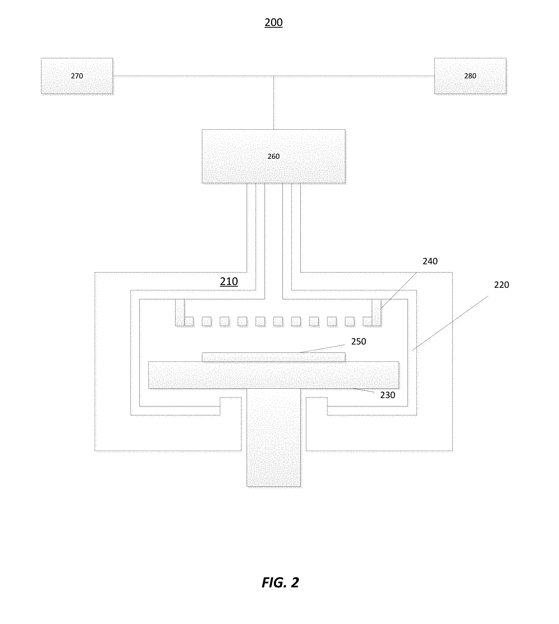
[0021] FIG. 2 illustrates another reactor 200 in accordance with at least one embodiment of the disclosure. The reactor 200 may comprise a reaction chamber 210, a reaction chamber lining 220, a susceptor 230, and a gas distribution structure (e.g., a showerhead 240). The reaction chamber lining 220 may be a coating comprising a material deposited onto the reaction chamber 210. Additionally or alternatively, the reactor 200 parts downstream and/or upstream from the reaction chamber, such as gas and pump lines, may be coated as well. Similar to reactor 100, although illustrated as a vertical-flow reactor with showerhead 240, reactor 200 may alternatively comprise a cross-flow reaction chamber instead of the showerhead type of reaction chamber. The showerhead 240 may disperse gas precursors that come from a remote plasma unit 260 and/or first or second gas sources, described below. The susceptor 230 holds a substrate 250 that is to be processed.
[0022] The reactor 200 may also comprise a first gas source 270 and a second gas source 280. The first gas source 270 and the second gas source 280 are illustrated as feeding gas to the remote plasma unit 260, but may additionally or alternatively provide gas directly to the reaction chamber 210 without passing through the remote plasma unit 260. The first gas source 270 and/or the second gas source 280 may provide a metal halide gas, such as a transition metal or aluminum halide, such as fluorine, chlorine or bromine comprising one or more of TiCl.sub.4, TiF.sub.4, TiCl.sub.x, TiF.sub.x, MoCl.sub.x, MoF.sub.x, WCl.sub.x, WF.sub.x, NbCl.sub.x, NbF.sub.x, TaCl.sub.x, TaF.sub.x, VCl.sub.x, VF.sub.x, AlCl.sub.x, HfCl.sub.x, or ZrCl.sub.x, for example. First gas source 270 and/or second gas source 280 may provide halide gas comprising non-metal halides like SbF.sub.5, organic halides like CCl.sub.4 or metaloxyhalides, such as WOF.sub.4, for example. Precursors from the first gas source 270 and/or the second gas source 280 can react with the chamber lining 220 to form gas compounds, with high saturation vapor pressure, in order to allow efficient purging, no or little condensation, as well as for contaminants to stay low within the reaction chamber 210. The first and the second gas sources 270, 280 may provide precursor containing at least one halide atom, such as chlorine, fluorine and/or bromine, for example, NbF.sub.5 or CCl.sub.4.
[0023] Components, including lining 220, of the reactor 200 may be made of materials that react with the precursors from one or more gas sources 270, 280 (e.g., one or more metal halide gases) to form (e.g., volatile) gas compounds. In particular, the reaction chamber lining 220, the susceptor 230, and/or the showerhead 240 can be made of materials that would react with the first and/or second precursor to form the gas compounds. The materials can include at least one of: tungsten; molybedenum; titanium; niobium; tantalum; vanadium; aluminum; hafnium; zirconium; zinc; vanadium alloy; zinc alloy; quartz; borosilicate quartz; stainless steel, for example. Other components of the reactor 200 that can be made of and/or coated with the materials listed above include gas lines, gas distribution blocks, heater plates, and gaskets, as each of these are capable of being sources of contamination. In accordance with some embodiments, the components made of and/or coated with material that reacts with first and/or second precursor comprise surfaces of components located below or downstream from showerhead plate up to a pumpline. In accordance with exemplary embodiments, the components made of and/or coated with material that reacts with the first and/or second precursor comprise surfaces of components located downstream from the point in which gases are entering the space above showerhead plate up to the pumpline. In some embodiments the components made of and/or coated with material that reacts with the first and/or second precursor comprise surfaces of components located downstream from the point of last valve before the reaction chamber up to the pumpline. In some embodiments, the components made of and/or coated with material that reacts with the first and/or second precursor comprise surfaces of components located downstream from the point of a second-to-last valve before the reaction chamber up to the pumpline. In some embodiments, the components made of and/or coated with material that reacts with the first and/or second precursor comprise surfaces of components located within a region having temperature difference between the reaction chamber temperature and edge of a reaction region of less than about 400.degree. C., less than about 300.degree. C., less than about 200.degree. C., less than about 150.degree. C., less than about 100.degree. C., less than about 50.degree. C. or less than about 25.degree. C. The point of a pumpline can be considered to be a point downstream from the reaction chamber or substrate from which point the chemicals, reaction by-products, particles or other materials cannot anymore affect the product or substrate in the reaction chamber or the reaction chamber lifetime in a detrimental way or have any other detrimental effects to the process, product, substrate or operation of the reactor.
[0024] The reaction chamber lining 220 may be formed on surfaces within the reaction chamber 210 using various methods, including, for example, atomic layer deposition (ALD) and/or chemical vapor deposition (CVD) and/or by liquid coating/deposition methods, such as electrodeposition. The reaction chamber lining 220 can have a thickness ranging between 0.1 mm and 10 mm, between 0.5 and 5 mm, between 1 and 3 mm, between 0.0001 and 0.001 mm, between 0.001 and 0.01 mm, or between 0.01 and 0.1 mm, or in some instances below 10 mm, but greater than about 10 nm, greater than about 100 nm, greater than about 1 .mu.m, greater than about 10 .mu.m or greater than about 100 .mu.m. With these thicknesses, the lifetime of the chamber can be quite long as the etch rate could be significantly less, on the order of 1-10 nm/min or even less, leading to a lifetime ranging between 1-5 years or more than about 1 week, more than about 1 month, more than about 0.5 years, more than about 1 year, more than about 2 years, more than about 3 years, more than about 4 years or more than about 5 years. In some embodiments, the etch rate of the reaction chamber material or lining is from about 0.1 to about 100 nm/min, about 0.5 to about 50 nm/min, about 1 to about 50 nm/min or more than 0.1 nm/min, but less than about 5 nm/min, less than about 10 nm/min, less than about 25 nm/min, less than about 50 nm/min or less than about 100 nm/min. In some embodiments the etch rate of the reaction chamber material or lining is from about 0.001 to about 10 nm, from about 0.01 to about 5 nm, from about 0.02 to about 2 nm, from about 0.02 to about 1 nm per one pulse or cycle of the etching chemical, or more than 0.001 nm/min per one pulse or cycle of the etching chemical, but less than about 10 nm, less than about 5 nm, less than about 1 nm, less than about 0.5 nm, or less than about 0.1 nm per one pulse or cycle of the etching chemical.
[0025] By applying or utilizing a reaction chamber material and/or lining/coating that is etched by one or more or combination of reaction gases (e.g., precursors derived from one or more gases from the gas sources, such as gas sources 160, 170, 270, 280), the impurity or contamination level of substrate that is etched can be effectively reduced. In some embodiments, when the reaction chamber material or lining/coating which is etched by one or more or combination of reaction gases, the substrate has less than about 5 at-%, less than about 1 at-%, less than about 0.5 at-%, less than about 0.1 at-%, less than about 0.05 at-%, less than about 0.01 at-%, less than about 0.005 at-% or less than about 0.001 at-% of impurities from reaction chamber, for example, as a metal contamination. In some instances, when the reaction chamber material or lining/coating which is etched by one or more or combination of reaction gases, the substrate has less than 10000 ppm, less than 1000 ppm, less than 100 ppm, less than 50 ppm or less than 10 ppm or in some cases undetectable amount impurities from reaction chamber, for example, as a metal contamination.
[0026] The particular implementations shown and described are illustrative of the invention and its best mode and are not intended to otherwise limit the scope of the aspects and implementations in any way. Indeed, for the sake of brevity, conventional manufacturing, connection, preparation, and other functional aspects of the system, reactor, or method may not be described in detail. Furthermore, the connecting lines shown in the various figures are intended to represent exemplary functional relationships and/or physical couplings between the various elements. Many alternative or additional functional relationships or physical connections may be present in the practical system, and/or may be absent in some embodiments.
[0027] It is to be understood that the configurations and/or approaches described herein are exemplary in nature, and that these specific embodiments or examples are not to be considered in a limiting sense, because numerous variations are possible. The specific routines or methods described herein may represent one or more of any number of processing strategies. Thus, the various acts illustrated may be performed in the sequence illustrated, in other sequences, or omitted in some cases.
[0028] The subject matter of the present disclosure includes all novel and nonobvious combinations and subcombinations of the various processes, systems, reactors, and configurations, and other features, functions, acts, and/or properties disclosed herein, as well as any and all equivalents thereof.
* * * * *
D00000
D00001
D00002
XML
uspto.report is an independent third-party trademark research tool that is not affiliated, endorsed, or sponsored by the United States Patent and Trademark Office (USPTO) or any other governmental organization. The information provided by uspto.report is based on publicly available data at the time of writing and is intended for informational purposes only.
While we strive to provide accurate and up-to-date information, we do not guarantee the accuracy, completeness, reliability, or suitability of the information displayed on this site. The use of this site is at your own risk. Any reliance you place on such information is therefore strictly at your own risk.
All official trademark data, including owner information, should be verified by visiting the official USPTO website at www.uspto.gov. This site is not intended to replace professional legal advice and should not be used as a substitute for consulting with a legal professional who is knowledgeable about trademark law.