Thermoelectric Conversion Element And Method For Producing The Same
BANIECKI; John David ; et al.
U.S. patent application number 16/416182 was filed with the patent office on 2019-09-12 for thermoelectric conversion element and method for producing the same. The applicant listed for this patent is FUJITSU LIMITED. Invention is credited to John David BANIECKI, Masatoshi ISHII, Kazuaki KURIHARA.
| Application Number | 20190280180 16/416182 |
| Document ID | / |
| Family ID | 54018248 |
| Filed Date | 2019-09-12 |


| United States Patent Application | 20190280180 |
| Kind Code | A1 |
| BANIECKI; John David ; et al. | September 12, 2019 |
THERMOELECTRIC CONVERSION ELEMENT AND METHOD FOR PRODUCING THE SAME
Abstract
A thermoelectric conversion element includes a film composed of a conductive oxide, a first electrode disposed on one end of the film composed of the conductive oxide, and a second electrode disposed on another end of the film composed of the conductive oxide, wherein the conductive oxide has a tetragonal crystal structure expressed by ABO.sub.3-x, where 0.1<x<1, wherein the conductive oxide has a band structure in which a Fermi level intersects seven bands between a .GAMMA. point and an R point, and wherein the first electrode and the second electrode are disposed on the film composed of the conductive oxide so that electrical charge moves in a direction of a smallest vector among three primitive translation vectors of the crystal structure.
| Inventors: | BANIECKI; John David; (Zama, JP) ; ISHII; Masatoshi; (Kawasaki, JP) ; KURIHARA; Kazuaki; (Atsugi, JP) | ||||||||||
| Applicant: |
|
||||||||||
|---|---|---|---|---|---|---|---|---|---|---|---|
| Family ID: | 54018248 | ||||||||||
| Appl. No.: | 16/416182 | ||||||||||
| Filed: | May 18, 2019 |
Related U.S. Patent Documents
| Application Number | Filing Date | Patent Number | ||
|---|---|---|---|---|
| 14636629 | Mar 3, 2015 | 10347810 | ||
| 16416182 | ||||
| Current U.S. Class: | 1/1 |
| Current CPC Class: | H01L 35/22 20130101; H01L 35/34 20130101; H01L 35/32 20130101 |
| International Class: | H01L 35/34 20060101 H01L035/34; H01L 35/22 20060101 H01L035/22; H01L 35/32 20060101 H01L035/32 |
Foreign Application Data
| Date | Code | Application Number |
|---|---|---|
| Mar 6, 2014 | JP | 2014-044141 |
Claims
1-6. (canceled)
7. A method for producing a thermoelectric conversion element, the method comprising: disposing a first electrode on one end of a film composed of a conductive oxide; and disposing a second electrode on another end of the film composed of the conductive oxide, wherein the conductive oxide has a tetragonal crystal structure expressed by ABOJ-x, where 0.1<x<1, wherein the conductive oxide has a band structure in which a Fermi level intersects seven bands between a r point and an R point, wherein the first electrode and the second electrode are disposed on the film composed of the conductive oxide so that electrical charge moves in a direction of a smallest vector among three primitive translation vectors of the crystal structure.
8. The method for producing a thermoelectric conversion element according to claim 7, further comprising: forming the film composed of the conductive oxide on a substrate; forming a mask on the film composed of the conductive oxide; forming a conductive film on a side surface of the film composed of the conductive oxide, the side surface being a surface on which the first electrode or the second electrode is disposed, and on an upper surface of the mask; and removing the mask and a portion of the conductive film formed on the upper surface of the mask to leave the remaining portion of the conductive film as the first electrode and the second electrode.
9. The method for producing a thermoelectric conversion element according to claim 7, wherein A of AB03-x expressing the crystal structure is Sr.
10. The method for producing a thermoelectric conversion element according to claim 7, wherein B of AB03-x expressing the crystal structure is Ti.
11. The method for producing a thermoelectric conversion element according to claim 7, wherein the Fermi level of the conductive oxide is higher than a lowest conduction band of the conductive oxide by 0.15 eV or more.
12. The method for producing a thermoelectric conversion element according to claim 7, wherein a defect band of the conductive oxide is higher than a lowest conduction band of the conductive oxide by 0.2 eV or more.
Description
CROSS-REFERENCE TO RELATED APPLICATION
[0001] This application is based upon and claims the benefit of priority of the prior Japanese Patent Application No. 2014-044141, filed on Mar. 6, 2014, the entire contents of which are incorporated herein by reference.
FIELD
[0002] The embodiments discussed herein are related to a thermoelectric conversion element, a method for producing the thermoelectric conversion element, and the like.
BACKGROUND
[0003] Recently, attention has been focused on use of SrTiO.sub.3 as a material for thermoelectric conversion elements because SrTiO.sub.3 has a high power factor and causes a low environmental load (for example, see Japanese Laid-open Patent Publication No. 5-218511, Japanese Laid-open Patent Publication No. 2012-186230, and J. D. Baniecki et al., Journal of Applied Physics 113, 013701, 2013).
[0004] However, it has been difficult to realize a sufficient thermoelectric performance even using a thermoelectric conversion element including SrTiO.sub.3.
[0005] Accordingly it is desired a thermoelectric conversion element that allows a higher thermoelectric performance to be achieved, a method for producing such a thermoelectric conversion element, and the like.
SUMMARY
[0006] According to an aspect of the invention, a thermoelectric conversion element includes a film composed of a conductive oxide, a first electrode disposed on one end of the film composed of the conductive oxide, and a second electrode disposed on another end of the film composed of the conductive oxide, wherein the conductive oxide has a tetragonal crystal structure expressed by ABO.sub.3-x, where 0.1<x<1, wherein the conductive oxide has a band structure in which a Fermi level intersects seven bands between a .GAMMA. point and an R point, and wherein the first electrode and the second electrode are disposed on the film composed of the conductive oxide so that electrical charge moves in a direction of a smallest vector among three primitive translation vectors of the crystal structure.
[0007] The object and advantages of the invention will be realized and attained by means of the elements and combinations particularly pointed out in the claims.
[0008] It is to be understood that both the foregoing general description and the following detailed description are exemplary and explanatory and are not restrictive of the invention, as claimed.
BRIEF DESCRIPTION OF DRAWINGS
[0009] FIG. 1 is a cross-sectional view of a thermoelectric conversion element according to the first embodiment, which illustrates the structure of the thermoelectric conversion element;
[0010] FIG. 2A is a diagram illustrating the band structure of SrTiO.sub.2.875;
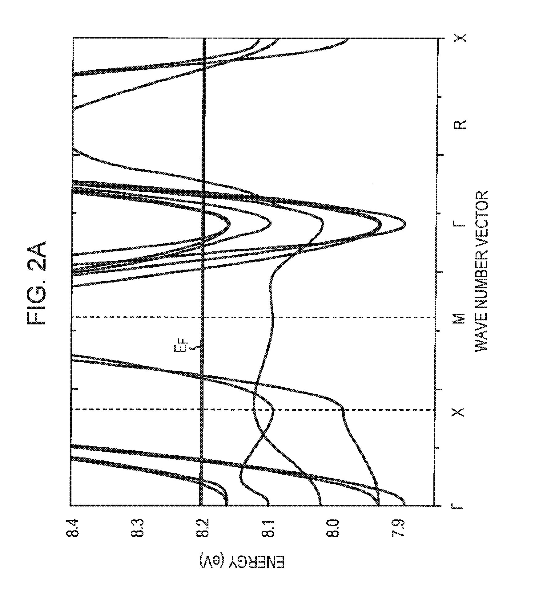
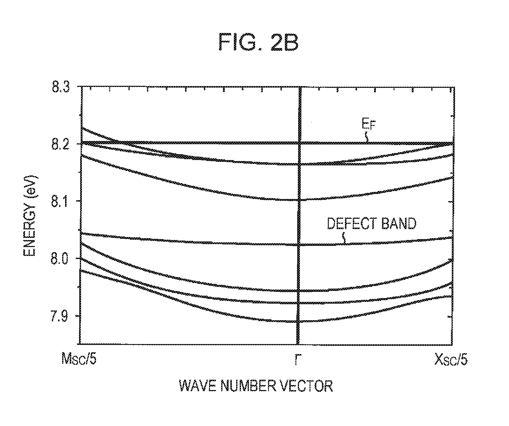
[0011] FIG. 2B is a diagram illustrating the band structure of SrTiO.sub.2.875;
[0012] FIGS. 3A to 3D are cross-sectional views of a thermoelectric conversion element according to the first embodiment, which illustrate steps of a method for producing the thermoelectric conversion element in order;
[0013] FIG. 4 is a cross-sectional view of a thermoelectric conversion device according to the second embodiment, which illustrates the structure of the thermoelectric conversion device;
[0014] FIG. 5 is a diagram illustrating an example of use of a thermoelectric conversion device according to the second embodiment; and
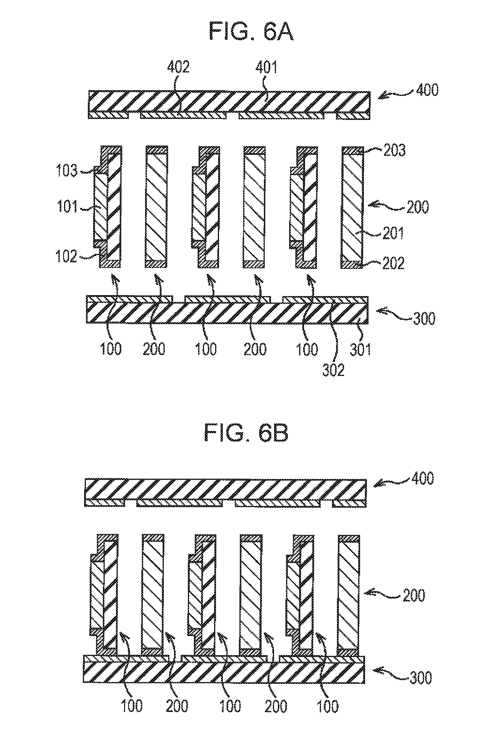
[0015] FIGS. 6A and 6B are cross-sectional views of a thermoelectric conversion device according to the second embodiment, which illustrate steps of a method for producing the thermoelectric conversion device in order.
DESCRIPTION OF EMBODIMENTS
[0016] Hereinafter, the embodiments discussed herein are described specifically with reference to the attached drawings.
First Embodiment
[0017] The first embodiment is described below. The first embodiment relates to a thermoelectric conversion element. FIG. 1 is a cross-sectional view of the thermoelectric conversion element according to the first embodiment, which illustrates the structure of the thermoelectric conversion element.
[0018] As illustrated in FIG. 1, a thermoelectric conversion element 100 according to the first embodiment includes a conductive oxide film 101 formed on a substrate 104, an electrode 102 disposed on one end of the conductive oxide film 101, and an electrode 103 disposed on the other end of the conductive oxide film 101.
[0019] The conductive oxide film 101 is composed of a conductive oxide, which has a tetragonal crystal structure expressed by ABO.sub.3-x (0.1<x<1). The electrodes 102 and 103 are disposed on the conductive oxide film 101 so that electrical charge moves in the direction of the smallest vector among three primitive translation vectors of the crystal structure. The conductive oxide has a band structure in which the Fermi level intersects seven bands between the r point and the R point.
[0020] For example, the conductive oxide film 101 is composed of SrTiO.sub.2.875 (x=0.125). The lengths of the three axes of the unit crystal lattice of SrTiO.sub.2.875 are about 3.849 .ANG., 3.849 .ANG., and 3.860 .ANG., and the electrodes 102 and 103 are disposed on the conductive oxide film 101 so that electrical charge moves in a direction parallel to the axis having a length of about 3.849 .ANG.. As illustrated in FIG. 2A, SrTiO.sub.2.875 has a band structure in which the Fermi level E.sub.F intersects seven bands between the .GAMMA. point and the R point.
[0021] Generally, power factor PF is calculated as PF=S.sup.2.times..sigma., where S represents the Seebeck coefficient and .sigma. represents electric conductivity. The larger the number of bands that intersect the Fermi level between the .GAMMA. point and the R point, the higher the Seebeck coefficient. The number of such bands is seven in the first embodiment while the number of such bands is six in SrTiO.sub.3. Thus, according to the first embodiment, a Seebeck coefficient S and a power factor PF that are higher than those of a thermoelectric conversion element including SrTiO.sub.3 may be achieved.
[0022] In a conductive oxide having a band structure in which the Fermi level intersects seven bands between the .GAMMA. point and the R point, the Fermi level is higher than the lowest conduction band by 0.15 eV or more and the defect band is higher than the lowest conduction band by 0.2 eV or more. In FIGS. 2A and 2B, the Fermi level E.sub.F is higher than the lowest conduction band by 0.15 eV or more. This allows a high thermoelectric performance to be realized.
[0023] The value of x in ABO.sub.3-x is more than 0.1 because, if x is 0.1 or less, a sufficiently high power factor PF may fail to be achieved due to an insufficient amount of oxygen vacancies. The value of x in ABO.sub.3-x is less than 1 because, if x is 1 or more, a sufficiently high power factor PF may fail to be achieved due to an excessive amount of oxygen vacancies, which results in the inconsistency of characteristics of the thermoelectric conversion element.
[0024] FIG. 7 summarizes the characteristics of various materials having a tetragonal crystal structure expressed by ABO.sub.3-x. In FIG. 7, S.sub.L and S.sub.S represent the Seebeck coefficients measured in a direction parallel to the longest axis among three axes of the unit crystal lattice, that is, the L-direction, and in a direction parallel to the shortest axis among three axes of the unit crystal lattice, that is, the S-direction, respectively. In FIG. 7, .sigma..sub.L/.tau..sub.0 and .sigma..sub.S/.tau..sub.0 represent values obtained by dividing electric conductivities measured in the L-direction and S-direction by relaxation time .tau..sub.0, respectively. In FIG. 7, PF.sub.L and PF.sub.S represent power factors measured in the L-direction and S-direction, respectively, which are calculated as PF.sub.L=S.sub.L.sup.2.times..sigma..sub.L/.tau..sub.0 and PF.sub.S=S.sub.S.sup.2.times..sigma..sub.S/.tau..sub.0.
TABLE-US-00001 TABLE 1-1 .sigma..sub.L/.tau..sub.0 .sigma..sub.S/.tau..sub.0 No. Composition S.sub.L (.mu.V/K) S.sub.S (.mu.V/K) (.times.10.sup.19 Sm.sup.-1sec.sup.-1) (.times.10.sup.19 Sm.sup.-1sec.sup.-1) 1 SrTiO.sub.2.875 -37.68 -36.64 8.14 12.88 2 Sr.sub.0.875La.sub.0.125TiO.sub.3 -41.3 -41.3 8.10 8.10 3 Sr.sub.0.5La.sub.0.5TiO.sub.3 -11.67 -11.67 25.90 25.90 4 SrTiO.sub.2.9375 -40.3 -39.1 6.14 8.88 5 SrTiO.sub.2.00 -14.5 -10.6 64.20 122.2
TABLE-US-00002 TABLE 1-2 PF.sub.L/.tau..sub.0 PF.sub.S/.tau..sub.0 No. (.times.10.sup.10 Wm.sup.-1K.sup.-2sec.sup.-1) (.times.10.sup.10 Wm.sup.-1K.sup.-2sec.sup.-1) Remarks 1 11.56 16.4 Example 2 13.81 13.81 Comparative example 3 3.53 3.53 Comparative example 4 9.97 13.58 Comparative example 5 13.5 13.73 Comparative example
[0025] As summarized in Tables 1-1 and 1-2, a markedly high power factor is obtained in the S direction of SrTiO.sub.2.875. Note, each values in the row of No. 1 in the tables 1-1 and 1-2 indicate the values of SrTiO.sub.2.875, and the values in the row of No. 2 indicate the values of Sr.sub.0.875La.sub.0.125TiO.sub.3, for example.
[0026] The thermoelectric conversion element 100 according to the first embodiment may be used as an n-type thermoelectric conversion element.
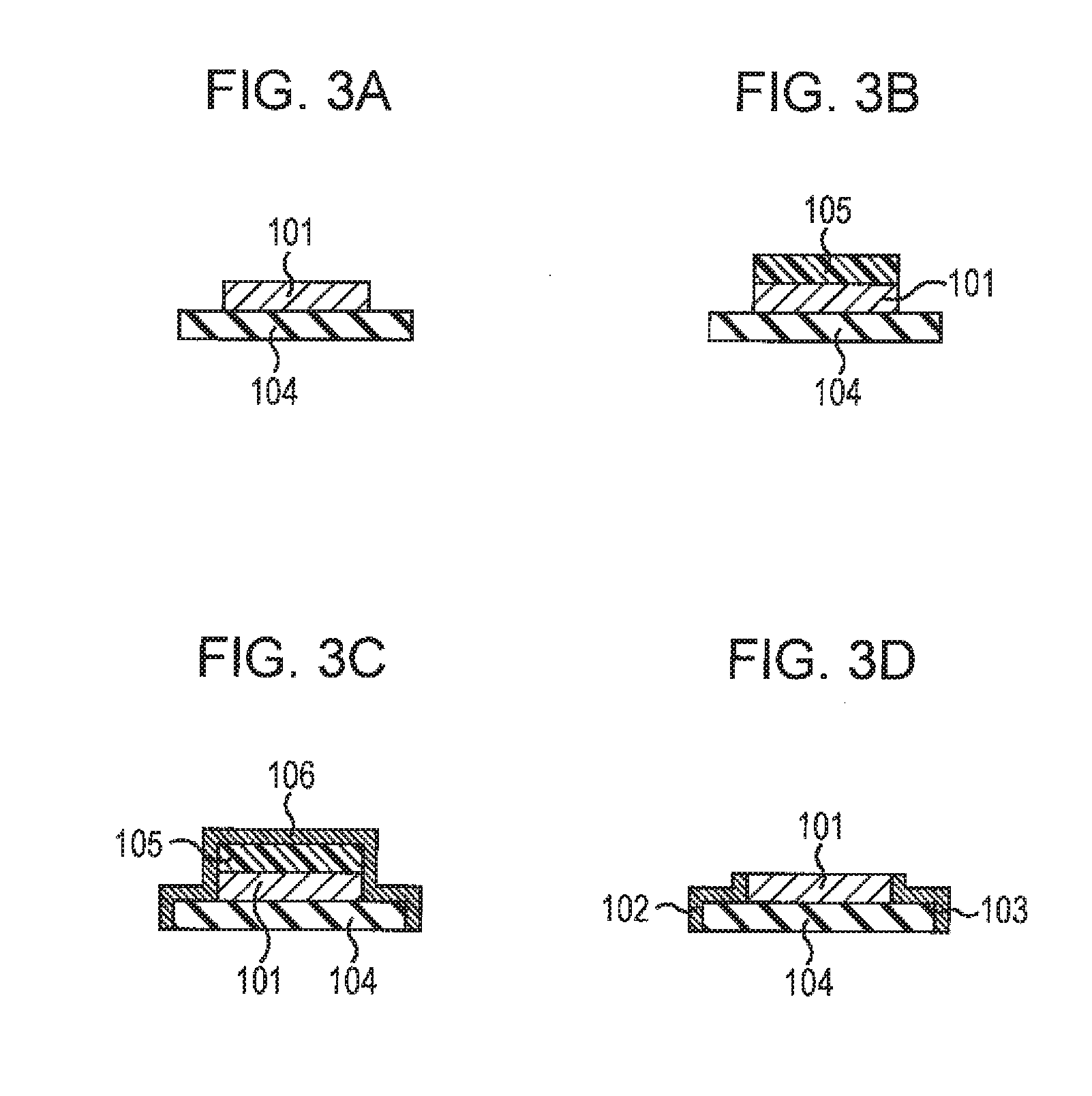
[0027] A method for producing the thermoelectric conversion element according to the first embodiment is described below. FIGS. 3A to 3D are cross-sectional views of the thermoelectric conversion element according to the first embodiment, which illustrate steps of the method for producing the thermoelectric conversion element in order.
[0028] As illustrated in FIG. 3A, a conductive oxide film 101 including oxygen vacancies is formed on a substrate 104. The substrate 104 may be, for example, a single-crystal substrate of (La.sub.0.3Sr.sub.0.7)(Al.sub.0.65Ta.sub.0.35)O.sub.3 (LSAT). The planar shape of the substrate 104 may be, for example, 15-mm square. The thickness of the substrate 104 may be, for example, 0.5 mm.
[0029] An SrTiO.sub.2.5 film that serves as the conductive oxide film 101 may be formed, for example, under the following conditions. An SrTiO.delta. single-crystal film is formed using an SrTiO.sub.3 target and a Q-switch Nd:YAG laser at a pulse rate of 10 Hz with an irradiation energy of 0.62 J/cm.sup.2. The spacing between the substrate 104 and the target is set to, for example, 5 cm. The temperature of the substrate 104 is set to, for example, 900.degree. C. The pressure inside the chamber is set to, for example, 10.sup.-6 Torr. After the single-crystal film is formed, the temperature is kept at 900.degree. C., the pressure inside the chamber is reduced to 10.sup.-9 Torr, and the resulting substrate is maintained for 3 hours. The substrate may optionally be annealed in an atmosphere including a reducing gas after the formation of the single-crystal film, which increases the amount of oxygen vacancies. For example, the substrate may be annealed in a 95-vol % Ar and 5-vol % H.sub.2 mixed gas atmosphere at 1 atm. An oxygen gas may optionally be charged into the chamber during the formation of the single-crystal film, which reduces the amount of oxygen vacancies. For example, during the formation of the single-crystal film, the temperature of the substrate 104 is set to 600.degree. C. and the oxygen pressure inside the chamber is set to 50 mTorr. The irradiation energy may be set to 0.4 J/cm.sup.2.
[0030] After the formation of the conductive oxide film 101, as illustrated in FIG. 313, a mask 105 is formed on the conductive oxide film 101. The mask 105 may be, for example, a metal mask or a photoresist mask.
[0031] As illustrated in FIG. 3C, a conductive film 106 is formed on the upper and side surfaces of the mask 105, the side surface of the conductive oxide film 101, and the upper and side surfaces of the substrate 104. The conductive film 106 is, for example, a multilayer body including a Cr film having a thickness of 25 nm and an Au film having a thickness of 500 nm which are formed by sputtering. At this time, for example, the RF power is set to 80 W, the temperature is set to room temperature (about 25.degree. C.), and the atmosphere is set to a 0.1-Pa Ar gas atmosphere.
[0032] As illustrated in FIG. 3D, subsequently, the mask 105 and a portion of the conductive film 106 formed on the upper and side surfaces of the mask 105 are removed. As a result, the remaining portion of the conductive film 106 is left on the side surface of the conductive oxide film 101 and the upper and side surfaces of the substrate 104, which serve as the electrode 102 and the electrode 103.
[0033] Thus, the thermoelectric conversion element is produced.
Second Embodiment
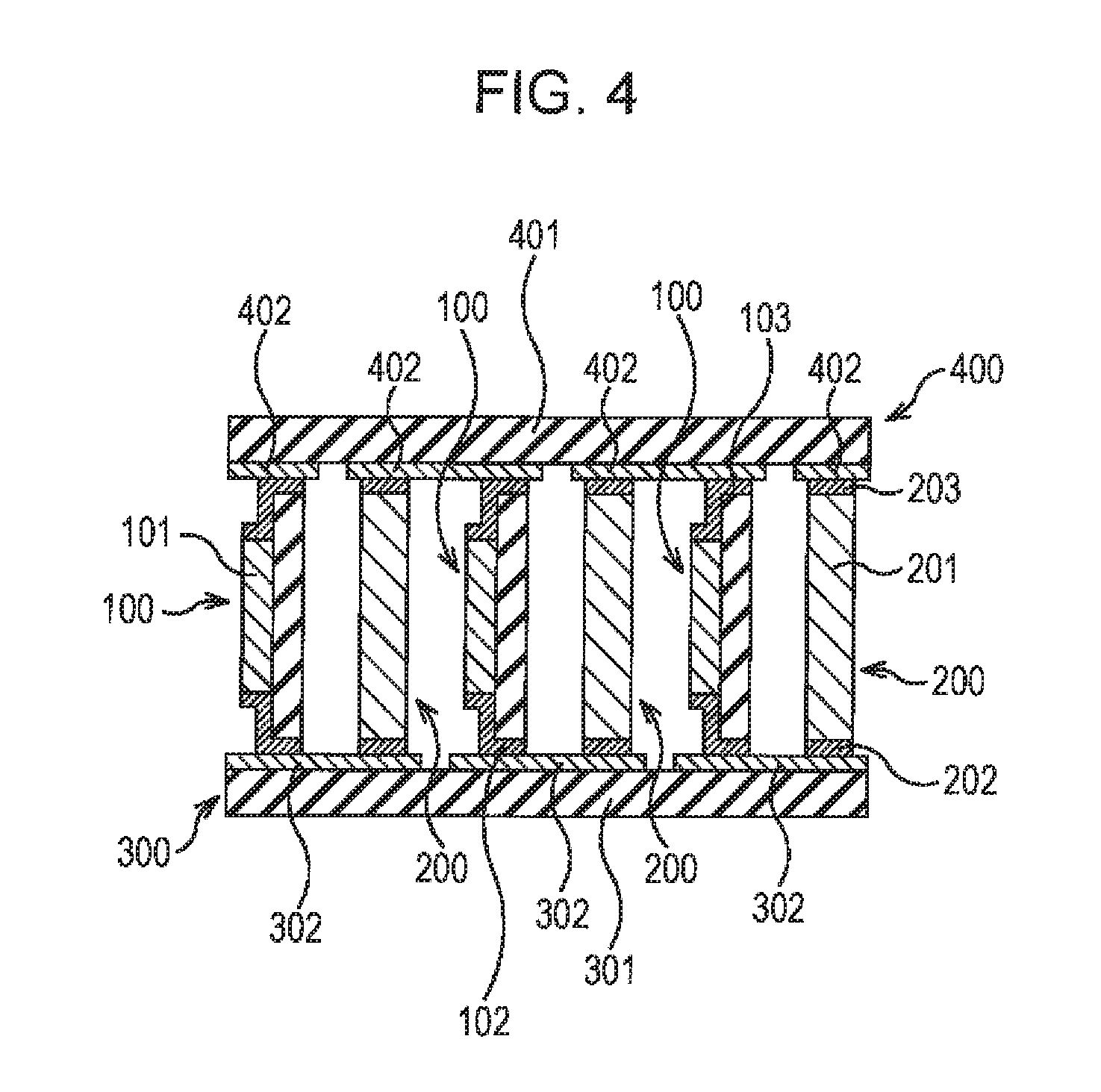
[0034] The second embodiment is described below. The second embodiment relates to a thermoelectric conversion device including the thermoelectric conversion element. FIG. 4 is a cross-sectional view of the thermoelectric conversion device according to the second embodiment, which illustrates the structure of the thermoelectric conversion device.
[0035] In the second embodiment, as illustrated in FIG. 4, a plurality of thermoelectric conversion elements 100 and a plurality of thermoelectric conversion elements 200 are disposed between a low-temperature-side substrate 300 and a high-temperature-side substrate 400. The low-temperature-side substrate 300 includes an insulating substrate 301 and a plurality of wires 302 formed on the insulating substrate 301. The high-temperature-side substrate 400 includes an insulating substrate 401 and a plurality of wires 402 formed on the insulating substrate 401. The thermoelectric conversion element 200 includes a p-type semiconductor film 201, an electrode 202 disposed on one end of the p-type semiconductor film 201, and an electrode 203 disposed on the other end of the p-type semiconductor film 201. The electrode 102 and the electrode 202 are connected to the wire 302, the electrode 103 and the electrode 203 are connected to the wire 402, and thereby the thermoelectric conversion elements 100 and the thermoelectric conversion elements 200 are alternately connected to each other in series.
[0036] In the thermoelectric conversion device, as illustrated in FIG. 5, a current flows when a load 500 is connected between two wires 402 located at the respective ends of the high-temperature-side substrate 400, heat is supplied from a heat source to the high-temperature-side substrate 400, and the low-temperature-side substrate 300 is provided so that heat is dissipated from the low-temperature-side substrate 300.
[0037] A method for producing the thermoelectric conversion device according to the second embodiment is described below. FIGS. 6A and 6B are cross-sectional views of the thermoelectric conversion device according to the second embodiment, which illustrates steps of the method for producing the thermoelectric conversion device in order.
[0038] As illustrated in FIG. 6A, thermoelectric conversion elements 100, thermoelectric conversion elements 200, a low-temperature-side substrate 300, and a high-temperature-side substrate 400 are prepared. A p-type semiconductor film 201 of the thermoelectric conversion element 200 may be, for example, a BiTe film. Electrodes 202 and Electrodes 203 may be, for example, multilayer bodies including a Cr film and a Au film similarly to the electrodes 102 and the electrodes 103 described above. An insulating substrate 301 and an insulating substrate 401 are preferably substrates having a high heat conductivity, such as SrTiO.sub.3 substrates. Wires 302 and 402 may be, for example, Cu wires.
[0039] As illustrated in FIG. 68, the electrodes 102 of the thermoelectric conversion elements 100 and the electrodes 202 of the thermoelectric conversion elements 200 are fixed to the respective wires 302 of the low-temperature-side substrate 300 using, for example, a conductive paste. Subsequently, the electrodes 103 of the thermoelectric conversion elements 100 and the electrodes 203 of the thermoelectric conversion elements 200 are fixed to the respective wires 402 of the high-temperature-side substrate 400.
[0040] Thus, the thermoelectric conversion device is produced.
[0041] The conductive oxide may be SrZrO.sub.3-x (0.1<x<1), Sr(Ti,Zr)O.sub.3-x (0.1<x<1), BaTiO.sub.3-x (0.1<x<1), BaZrO.sub.3-x (0.1<x<1), Ba(Ti,Zr)O.sub.3-x (0.1<x<1), (Ba,Sr)TiO.sub.3-x (0.1<x<1), (Ba,Sr)ZrO.sub.3-x (0.1<x<1), or (Ba,Sr)(Ti,Zr)O.sub.3-x (0.1<x<1). These conductive oxides may be doped with La and/or Nb. A method for forming the conductive oxide film is not particularly limited. The thickness of the conductive oxide film is not particularly limited.
[0042] All examples and conditional language recited herein are intended for pedagogical purposes to aid the reader in understanding the invention and the concepts contributed by the inventor to furthering the art, and are to be construed as being without limitation to such specifically recited examples and conditions, nor does the organization of such examples in the specification relate to a showing of the superiority and inferiority of the invention. Although the embodiments of the present invention have been described in detail, it should be understood that the various changes, substitutions, and alterations could be made hereto without departing from the spirit and scope of the invention.
* * * * *
D00000
D00001
D00002
D00003
D00004
D00005
D00006
D00007
XML
uspto.report is an independent third-party trademark research tool that is not affiliated, endorsed, or sponsored by the United States Patent and Trademark Office (USPTO) or any other governmental organization. The information provided by uspto.report is based on publicly available data at the time of writing and is intended for informational purposes only.
While we strive to provide accurate and up-to-date information, we do not guarantee the accuracy, completeness, reliability, or suitability of the information displayed on this site. The use of this site is at your own risk. Any reliance you place on such information is therefore strictly at your own risk.
All official trademark data, including owner information, should be verified by visiting the official USPTO website at www.uspto.gov. This site is not intended to replace professional legal advice and should not be used as a substitute for consulting with a legal professional who is knowledgeable about trademark law.