Method For Depositing A Metal Chalcogenide On A Substrate By Cyclical Deposition
Mattinen; Miika ; et al.
U.S. patent application number 16/417938 was filed with the patent office on 2019-09-05 for method for depositing a metal chalcogenide on a substrate by cyclical deposition. The applicant listed for this patent is ASM IP Holding B.V.. Invention is credited to Markku Leskela, Miika Mattinen, Mikko Ritala.
| Application Number | 20190272993 16/417938 |
| Document ID | / |
| Family ID | 65993432 |
| Filed Date | 2019-09-05 |


View All Diagrams
| United States Patent Application | 20190272993 |
| Kind Code | A1 |
| Mattinen; Miika ; et al. | September 5, 2019 |
METHOD FOR DEPOSITING A METAL CHALCOGENIDE ON A SUBSTRATE BY CYCLICAL DEPOSITION
Abstract
A method for depositing a metal chalcogenide on a substrate by cyclical deposition is disclosed. The method may include, contacting the substrate with at least one metal containing vapor phase reactant and contacting the substrate with at least one chalcogen containing vapor phase reactant. Semiconductor device structures including a metal chalcogenide deposited by the methods of the disclosure are also provided.
| Inventors: | Mattinen; Miika; (Helsinki, FI) ; Ritala; Mikko; (Espoo, FI) ; Leskela; Markku; (Espoo, FI) | ||||||||||
| Applicant: |
|
||||||||||
|---|---|---|---|---|---|---|---|---|---|---|---|
| Family ID: | 65993432 | ||||||||||
| Appl. No.: | 16/417938 | ||||||||||
| Filed: | May 21, 2019 |
Related U.S. Patent Documents
| Application Number | Filing Date | Patent Number | ||
|---|---|---|---|---|
| 15729485 | Oct 10, 2017 | 10319588 | ||
| 16417938 | ||||
| Current U.S. Class: | 1/1 |
| Current CPC Class: | C23C 16/56 20130101; H01L 29/66969 20130101; H01L 29/78696 20130101; C23C 16/306 20130101; H01L 21/02664 20130101; H01L 21/02381 20130101; H01L 21/02568 20130101; H01L 21/02488 20130101; C23C 16/45553 20130101; H01L 29/78681 20130101; H01L 29/778 20130101; C23C 16/30 20130101; H01L 21/0262 20130101; H01L 29/24 20130101; C23C 16/52 20130101; H01L 29/742 20130101 |
| International Class: | H01L 21/02 20060101 H01L021/02; C23C 16/30 20060101 C23C016/30; H01L 29/24 20060101 H01L029/24; C23C 16/56 20060101 C23C016/56; C23C 16/455 20060101 C23C016/455; H01L 29/786 20060101 H01L029/786 |
Claims
1. A method for depositing a metal chalcogenide on a substrate by cyclical deposition, the method comprising: contacting the substrate with at least one metal containing vapor phase reactant comprising, a partial chemical structure represented by the formula M-O--C, wherein "M" represents a metal atom, wherein "0" represents an oxygen atom, and wherein "C" represents a carbon atom, and wherein the metal atom is bonded to the oxygen atom, and wherein the oxygen atom is bonded to the carbon atom; and contacting the substrate with at least one chalcogen containing vapor phase reactant.
2. The method of claim 1, wherein the metal chalcogenide comprises a metal dichalcogenide.
3. The method of claim 1, wherein the at least one chalcogen containing vapor phase reactant comprises S, Se, or Te.
4. The method of claim 1, wherein the metal chalcogenide comprises an oxygen (O) content less than 10 atomic-%.
5. The method of claim 1, wherein the cyclical deposition comprises atomic layer deposition.
6. The method of claim 1, wherein the cyclical deposition comprises cyclical chemical vapor deposition.
7. The method of claim 1, wherein the metal containing vapor phase reactant comprises at least one of a tin (Sn) containing vapor phase reactant, or a germanium (Ge) containing vapor phase reactant.
8. The method of claim 7, wherein the at least one tin (Sn) containing vapor phase reactant is represented by the chemical formula Sn(OR).sub.x, wherein R is a C.sub.1-C.sub.5 alkyl group and x is an integer from 2-6.
9. The method of claim 7, wherein the at least one tin (Sn) containing vapor phase reactant comprises tin (IV) acetate.
10. The method of claim 7, wherein the at least one tin (Sn) containing vapor phase reactant is represented by the partial formula: ##STR00004## wherein a tin (Sn) atom is bonded to two oxygen (O) atoms, and said oxygen (O) atoms are bonded to a carbon atom (C) through one single bond and one double bond, and R comprises a hydrocarbon group.
11. The method of claim 7, wherein the at least one tin (Sn) containing vapor phase reactant is represented by the partial formula: ##STR00005## wherein a tin (Sn) atom is bonded to two oxygen (O) atoms, and said oxygen (O) atoms are bonded to a carbon atom (C) through one single bond and one double bond, and R is a hydrocarbon group, and L is a further hydrocarbon group.
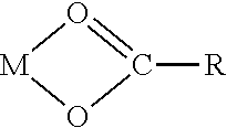
12. The method of claim 7, wherein the at least one tin (Sn) containing vapor phase reactant is represented by the partial chemical formula: L-Sn--O--C wherein a tin (Sn) atom is bonded to an oxygen (O) atom, and said oxygen (O) atom is bonded to a carbon atom (C), and L is a hydrocarbon group.
13. The method of claim 1, wherein the at least one chalcogen containing vapor phase reactant comprises hydrogen sulfide (H.sub.2S), hydrogen selenide (H.sub.2Se), dimethyl sulfide ((CH.sub.3).sub.2S), or dimethyl telluride (CH.sub.3).sub.2Te.
14. The method of claim 1, wherein the method comprises at least one deposition cycle in which the substrate is alternately and sequentially contacted with the at least metal containing vapor phase reactant and the at least one chalcogen containing vapor phase reactant.
15. The method of claim 14, wherein the deposition cycle is repeated two or more times.
16. The method of claim 1, further comprising heating the substrate to a temperature of approximately greater than 150.degree. C.
17. The method of claim 16, further comprising heating the substrate to a temperature of less than approximately 500.degree. C.
18. The method of claim 1, wherein the metal chalcogenide comprises tin disulfide.
19. The method of claim 1, wherein the metal chalcogenide comprises germanium disulfide.
20. The method of claim 1, further comprising a post-deposition annealing of the metal chalcogenide at a temperature between approximately 150.degree. C. and approximately 300.degree. C.
21. The method of claim 20, wherein the post-deposition annealing of the metal chalcogenide is performed in a hydrogen sulfide (H.sub.2S) atmosphere.
22. A semiconductor device structure comprising a metal chalcogenide deposited by the method of claim 1.
23. The semiconductor device structure of claim 24, wherein the metal chalcogenide comprises at least a portion of the channel region in a transistor structure.
24. A reaction system configured to perform the method of claim 1.
Description
CROSS REFERENCE TO RELATED APPLICATIONS
[0001] This application is a continuation of U.S. patent application Ser. No. 15/729,485 filed Oct. 10, 2017 and entitled "METHOD FOR DEPOSITING A METAL CHALCOGENIDE ON A SUBSTRATE BY CYCLICAL DEPOSITION," the disclosure of which is hereby incorporated by reference in its entirety for all purposes.
PARTIES OF JOINT RESEARCH AGREEMENT
[0002] The invention claimed herein was made by, or on behalf of, and/or in connection with a joint research agreement between the University of Helsinki and ASM Microchemistry Oy. The agreement was in effect on and before the date the claimed invention was made, and the claimed invention was made as a result of activities undertaken within the scope of the agreement.
FIELD OF INVENTION
[0003] The present disclosure relates generally to methods for depositing a metal chalcogenide on a substrate by cyclical deposition and particularly to the cyclical deposition of tin disulfide or germanium disulfide. The disclosure also relates to semiconductor device structures including a metal chalcogenide thin film formed by cyclical deposition.
BACKGROUND OF THE DISCLOSURE
[0004] The interest in two-dimensional (2D) materials has increased dramatically in recent years due to their potential in improving performance in next generation electronic devices. For example, graphene has been the most studied 2D material to date and exhibits high mobility, transmittance, mechanical strength and flexibility. However, the lack of a band gap in pure graphene has limited its performance in semiconductor device structures, such as transistors. Such limitations in graphene have stimulated research in alternative 2D materials as analogues of graphene. Recently, transition metal chalcogenides, and particularly transition metal dichalcogenides, have attracted considerable research attention as an alternative to graphene. Transition metal dichalcogenides may have stoichiometry of MX.sub.2, which describes a transition metal sandwiched between two layers of chalcogen atoms, with strong in-plane covalent bonding between the metal-chalcogen and weak out-of-plane van der Walls bonding between the layers.
[0005] However, there are few scalable, low temperature methods to produce 2D materials. Currently, mechanical exfoliation of bulk crystals is the most commonly used method of formation, but although this method produces good quality crystals, the method is unable to produce continuous films and is very labor intensive, making such a method not viable for industrial production. Chemical vapor deposition (CVD) has been used to deposit 2D materials, but current CVD processes for metal chalcogenides, such as, for example, tin disulfide (SnS.sub.2), operate at temperatures above 600.degree. C. and are unable to produce continuous, large area 2D materials. Accordingly, methods are desirable that are capable of producing 2D materials with a suitable band gap, at a reduced deposition temperature and with atomic level film thickness control.
SUMMARY OF THE DISCLOSURE
[0006] This summary is provided to introduce a selection of concepts in a simplified form. These concepts are described in further detail in the detailed description of example embodiments of the disclosure below. This summary is not intended to identify key features or essential features of the claimed subject matter, nor is it intended to be used to limit the scope of the claimed subject matter.
[0007] In some embodiments, methods for depositing a metal chalcogenide on a substrate by cyclical deposition are provided. The method may comprise; contacting the substrate with at least one metal containing vapor phase reactant comprising, a partial chemical structure represented by the chemical formula M-O--C wherein a metal atom is bonded to an oxygen atom (O), and said oxygen (O) atom is bonded to a carbon (C) atom; and contacting the substrate with at least one chalcogen containing vapor phase reactant. The embodiments of the disclosure also provide semiconductor device structures comprising a metal chalcogenide deposited by the methods described herein.
[0008] For the purpose of summarizing the invention and the advantages achieved over the prior art, certain objects and advantages of the invention have been described herein above. Of course, it is to be understood that not necessarily all such objects or advantages may be achieved in accordance with any particular embodiment of the invention. Thus, for example, those skilled in the art will recognize that the invention may be embodied or carried out in a manner that achieves or optimizes one advantage or group of advantages as taught or suggested herein without necessarily achieving other objects or advantages as may be taught or suggested herein.
[0009] All of these embodiments are intended to be within the scope of the invention herein disclosed. These and other embodiments will become readily apparent to those skilled in the art from the following detailed description of certain embodiments having reference to the attached figures, the invention not being limited to any particular embodiment(s) disclosed.
BRIEF DESCRIPTION OF THE DRAWING FIGURES
[0010] While the specification concludes with claims particularly pointing out and distinctly claiming what are regarded as embodiments of the invention, the advantages of embodiments of the disclosure may be more readily ascertained from the description of certain examples of the embodiments of the disclosure when read in conjunction with the accompanying drawings, in which:
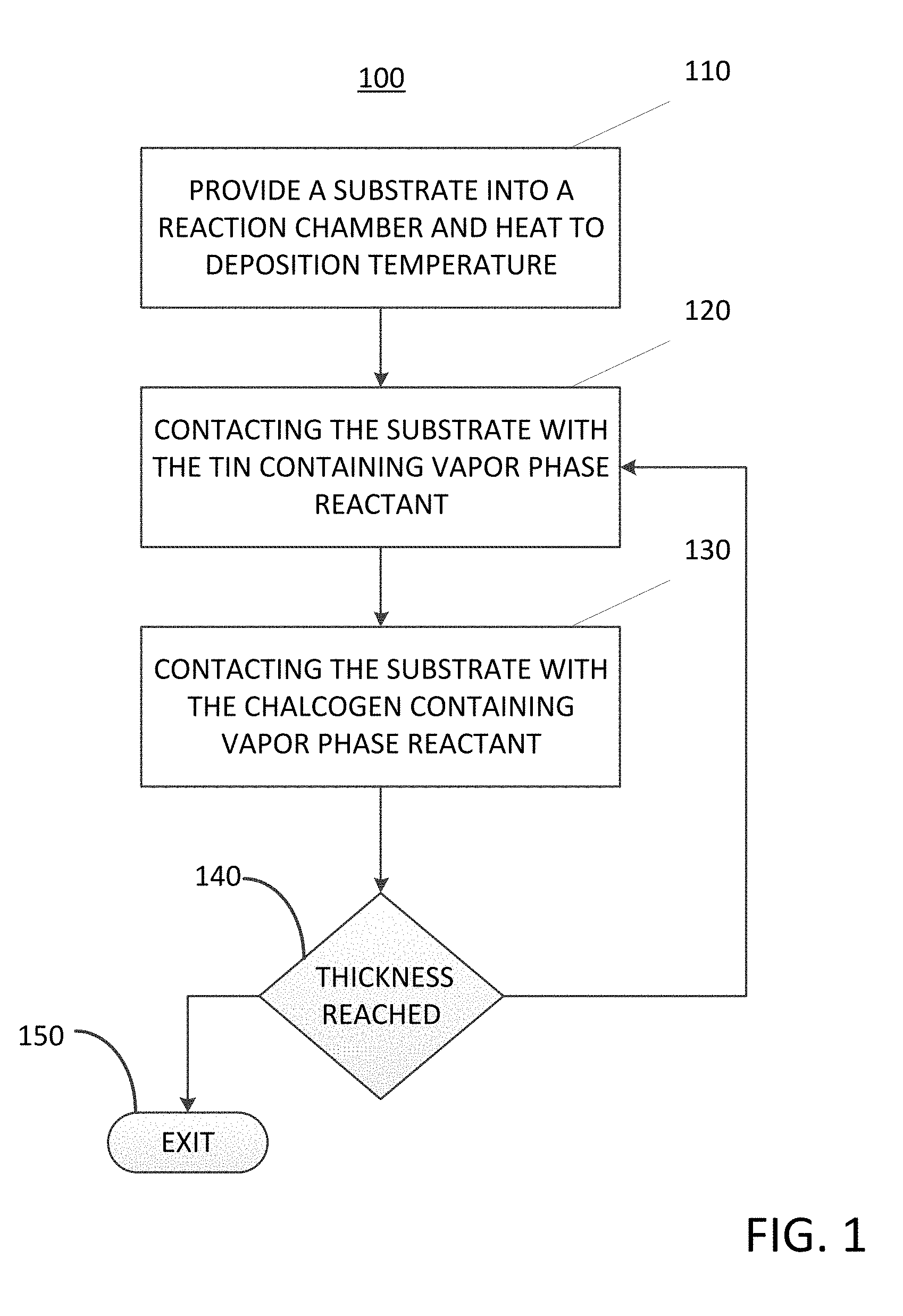
[0011] FIG. 1 is a process flow diagram illustrating an exemplary cyclical deposition method according to the embodiments of the disclosure;
[0012] FIG. 2 illustrates grazing incidence x-ray diffraction (GIXRD) data for tin dichalcogenide thin films deposited according to the embodiments of the disclosure;
[0013] FIG. 3 illustrates further grazing incidence x-ray diffraction (GIXRD) data for tin dichalcogenide thin films deposited according to the embodiments of the disclosure;
[0014] FIG. 4 is a high-angle annular dark-field scanning transmission electron microscopy (HAADF-STEM) image of a structure comprising a tin dichalcogenide 2D material deposited according to the embodiments of the disclosure;
[0015] FIG. 5 illustrates a Raman spectrum obtained from a tin dichalcogenide thin film deposited according to the embodiments of the disclosure;
[0016] FIG. 6 illustrates an exemplary semiconductor device structure including a metal chalcogenide thin film deposited according to the embodiments of the disclosure;
[0017] FIG. 7 illustrates an exemplary reaction system which may be used to deposit metal chalcogenide thin films according to the embodiments of the disclosure.
DETAILED DESCRIPTION OF EXEMPLARY EMBODIMENTS
[0018] Although certain embodiments and examples are disclosed below, it will be understood by those in the art that the invention extends beyond the specifically disclosed embodiments and/or uses of the invention and obvious modifications and equivalents thereof. Thus, it is intended that the scope of the invention disclosed should not be limited by the particular disclosed embodiments described below.
[0019] The illustrations presented herein are not meant to be actual views of any particular material, structure, or device, but are merely idealized representations that are used to describe embodiments of the disclosure.
[0020] As used herein, the term "substrate" may refer to any underlying material or materials that may be used, or upon which, a device, a circuit or a film may be formed.
[0021] As used herein, the term "cyclic deposition" may refer to the sequential introduction of precursors (reactants) into a reaction chamber to deposit a film over a substrate and includes deposition techniques such as atomic layer deposition and cyclical chemical vapor deposition.
[0022] As used herein, the term "atomic layer deposition" (ALD) may refer to a vapor deposition process in which deposition cycles, preferably a plurality of consecutive deposition cycles, are conducted in a process chamber. Typically, during each cycle the precursor is chemisorbed to a deposition surface (e.g., a substrate surface or a previously deposited underlying surface such as material from a previous ALD cycle), forming a monolayer or sub-monolayer that does not readily react with additional precursor (i.e., a self-limiting reaction). Thereafter, if necessary, a reactant (e.g., another precursor or reaction gas) may subsequently be introduced into the process chamber for use in converting the chemisorbed precursor to the desired material on the deposition surface. Typically, this reactant is capable of further reaction with the precursor. Further, purging steps may also be utilized during each cycle to remove excess precursor from the process chamber and/or remove excess reactant and/or reaction byproducts from the process chamber after conversion of the chemisorbed precursor. Further, the term "atomic layer deposition," as used herein, is also meant to include processes designated by related terms such as, "chemical vapor atomic layer deposition," "atomic layer epitaxy" (ALE), molecular beam epitaxy (MBE), gas source MBE, or organometallic MBE, and chemical beam epitaxy when performed with alternating pulses of precursor composition(s), reactive gas, and purge (e.g., inert carrier) gas.
[0023] As used herein, the term "cyclical chemical vapor deposition" may refer to any process wherein a substrate is sequentially exposed to two or more volatile precursors, which react and/or decompose on a substrate to produce a desired deposition.
[0024] As used herein, the term "chalcogen containing vapor phase reactant" may refer to a reactant (precursor) containing a chalcogen, wherein a chalcogen is an element from Group VI of the periodic including sulphur, selenium, and tellurium.
[0025] As used herein, the term "film" and "thin film" may refer to any continuous or non-continuous structures and material deposited by the methods disclosed herein. For example, "film" and "thin film" could include 2D materials, nanorods, nanotubes, or nanoparticles or even partial or full molecular layers or partial or full atomic layers or clusters of atoms and/or molecules. "Film" and "thin film" may comprise material or a layer with pinholes, but still be at least partially continuous.
[0026] As used herein, the term "partial chemical structure" may refer to the chemical structure of a portion of a chemical compound, i.e., the chemical structure of less than the whole chemical compound.
[0027] As used herein, the term "2D material" or "two-dimensional material" may refer to a nanometer scale crystalline material one, two or three atoms in thickness. In addition "2D materials" or "two-dimensional material" may also refer to an ordered nanometer scale crystalline structure composed of multiple monolayers of crystalline materials of approximately three atoms in thickness per monolayer.
[0028] The embodiments of the disclosure may include methods for depositing a metal chalcogenide on a substrate by cyclical deposition and particularly methods for depositing a tin disulfide (SnS.sub.2) thin film or a germanium disulfide (GeS.sub.2) thin film by atomic layer deposition processes. As a non-limiting example, Tin disulfide is an emerging material, which has a 2D crystal structure, similar to the well-known transition metal dichalcogenides (TMDCs), such as, for example, molybdenum disulfide (MoS.sub.2). In comparison to the most studied 2D material, graphene, tin disulfide has a sizable band gap (bulk .about.1.8-2.2 eV, monolayer 2.8 eV), which makes tin disulfide more suitable in semiconductor device structures, such as, for example, field effect transistors (FETs). Initial research involving tin disulfide as the channel material in a FET device have shown electrical properties comparable to molybdenum disulfide, such as, for example, a mobility up to 50-200 cm.sup.2V.sup.-1s.sup.-1 and on/off ratios of 10.sup.6 to 10.sup.8, as well as a strong photoresponsivity of 100 AW.sup.-1. Other possible application areas for tin disulfide thin films include, but are not limited to, catalysis, energy storage, and photovoltaics.
[0029] Current methods for forming a tin disulfide thin film are not suitable for forming high quality, conformal, low temperature thin films. Tin disulfide crystals may be formed by mechanical exfoliation of a bulk tin disulfide crystal, but such methods are not suitable for forming tin disulfide to a thickness accuracy on the atomic scale on suitable substrates. In addition, chemical vapor deposition of tin disulfide has been demonstrated but such processes operate at high deposition temperatures (greater than 600.degree. C.) and are unsuitable to produce nanoscale, conformal, thin films.
[0030] Cyclical deposition methods, such as cyclical chemical vapor deposition and atomic layer deposition techniques, are inherently scalable and offer atomically accurate film thickness control, which is crucial in the deposition of high quality 2D materials. In addition, cyclic deposition methods, such as atomic layer deposition, are characteristically conformal, thereby providing the ability to uniformly coat three dimensional structures. Atomic layer deposition of tin disulfide has been demonstrated utilizing Sn(NMe.sub.2).sub.4 and H.sub.2S as the tin and chalcogenide precursors respectively, Ham et al., ACS Applied Material Interfaces, 5, (2013) 8880. However, such prior art atomic layer deposition processes for forming tin disulfide may be problematic. For example, the tin disulfide may need to be deposited over a narrow temperature range and require post-deposition annealing processes to crystallize the tin disulfide. In addition, the Sn(NMe.sub.2).sub.4 precursor may be somewhat unstable, which may result in poor quality films over large area substrates, such as, for example, 200 mm or 300 mm substrates.
[0031] Accordingly, methods are desired which are capable of depositing metal dichalcogenide films at low temperature, conformally and with atomic thickness accuracy. In addition, semiconductor device structures comprising a metal dichalcogenide film are desirable.
[0032] A non-limiting example embodiment of a cyclical deposition process may include ALD, wherein ALD is based on typically self-limiting reactions, whereby sequential and alternating pulses of reactants are used to deposit about one atomic (or molecular) monolayer of material per deposition cycle. The deposition conditions and precursors are typically selected to provide self-saturating reactions, such that an absorbed layer of one reactant leaves a surface termination that is non-reactive with the vapor phase reactants of the same reactant. The substrate is subsequently contacted with a different reactant that reacts with the previous termination to enable continued deposition. Thus, each cycle of alternating pulsed reactants typically leaves no more than about one monolayer of the desired material. However, as mentioned above, the skilled artisan will recognize that in one or more ALD cycles more than one monolayer of material may be deposited, for example, if some gas phase reactions occur despite the alternating nature of the process.
[0033] In an ALD-type process for depositing a metal chalcogenide films, one deposition cycle may comprise exposing the substrate to a first reactant, removing any unreacted first reactant and reaction byproducts from the reaction space and exposing the substrate to a second reactant, followed by a second removal step. The first reactant may comprise a metal containing precursor, such as a tin or a germanium containing precursor, and the second reactant may comprise a chalcogen containing precursor.
[0034] Precursors may be separated by inert gases, such as argon (Ar) or nitrogen (N.sub.2), to prevent gas phase reactions between reactants and enable self-saturating surface reactions. In some embodiments, however, the substrate may be moved to separately contact a first vapor phase reactant and a second vapor phase reactant. Because the reactions self-saturate, strict temperature control of the substrates and precise dosage control of the precursor may not be required. However, the substrate temperature is preferably such that an incident gas species does not condense into monolayers nor decompose on the substrate surface. Surplus chemicals and reaction byproducts, if any, are removed from the substrate surface, such as by purging the reaction space or by moving the substrate, before the substrate is contacted with the next reactive chemical. Undesired gaseous molecules can be effectively expelled from the reaction space with the help of an inert purging gas. A vacuum pump may be used to assist in the purging process.
[0035] Reactors capable of being used to deposit or grow thin films can be used for the deposition. Such reactors include ALD reactors, as well as CVD reactors equipped with appropriate equipment and means for providing the precursors. According to some embodiments, a showerhead reactor may be used.
[0036] Examples of suitable reactors that may be used include commercially available single substrate (or single wafer) deposition equipment such as Pulsar.RTM. reactors (such as the Pulsar.RTM. 2000 and the Pulsar.RTM. 3000 and Pulsar.RTM. XP ALD), and EmerALD.RTM. XP and the EmerALD.RTM. reactors, available from ASM America, Inc. of Phoenix, Ariz. and ASM Europe B.V., Almere, Netherlands. Other commercially available reactors include those from ASM Japan K.K (Tokyo, Japan) under the tradename Eagle.RTM. XP and XP8. In some embodiments the reactor is a spatial ALD reactor, in which the substrates moves or rotates during processing.
[0037] In some embodiments a batch reactor may be used. Suitable batch reactors include, but are not limited to, Advance.RTM. 400 Series reactors commercially available from and ASM Europe B.V. (Almere, Netherlands) under the trade names A400 and A412 PLUS. In some embodiments, a vertical batch reactor is utilized in which the boat rotates during processing, such as the A412. Thus, in some embodiments, the wafers rotate during processing. In other embodiments, the batch reactor comprises a mini-batch reactor configured to accommodate 10 or fewer wafers, 8 or fewer wafers, 6 or fewer wafers, 4 or fewer wafers, or 2 wafers. In some embodiments in which a batch reactor is used, wafer-to-wafer non-uniformity is less than 3% (1 sigma), less than 2%, less than 1% or even less than 0.5%.
[0038] The deposition processes described herein can optionally be carried out in a reactor or reaction space connected to a cluster tool. In a cluster tool, because each reaction space is dedicated to one type of process, the temperature of the reaction space in each module can be kept constant, which improves the throughput compared to a reactor in which the substrate is heated up to the process temperature before each run. Additionally, in a cluster tool it is possible to reduce the time to pump the reaction space to the desired process pressure levels between substrates.
[0039] A stand-alone reactor can be equipped with a load-lock. In that case, it is not necessary to cool down the reaction space between each run. In some embodiments, a deposition process for depositing a thin film comprising a metal dichalcogenide thin film may comprise a plurality of deposition cycles, for example ALD cycles.
[0040] In some embodiments, cyclical deposition processes are used to form metal chalcogenide thin films on a substrate and the cyclical deposition process may be an ALD type process. In some embodiments, the cyclical deposition may be a hybrid ALD/CVD or cyclical CVD process. For example, in some embodiments the deposition or growth rate of the ALD process may be low compared with a CVD process. One approach to increase the growth rate may be that of operating at a higher substrate temperature than that typically employed in an ALD process, resulting in a chemical vapor deposition process, but still taking advantage of the sequential introduction or precursor, such a process may be referred to as cyclical CVD.
[0041] According to some embodiments of the disclosure, ALD processes are used to form metal chalcogenide thin films on a substrate, such as an integrated circuit workpiece. In some embodiments, each ALD cycle may comprise two distinct deposition steps or phases. In a first phase of the deposition cycle ("the metal phase"), the substrate surface on which deposition is desired is contacted with a first vapor phase reactant comprising at least one tin (Sn) containing vapor phase reactant or at least one germanium (Ge) containing vapor phase reactant which chemisorbs onto the substrate surface, forming no more than about one monolayer of reactant species on the surface of the substrate. In a second phase of the deposition cycle ("the chalcogen phase"), the substrate surface on which deposition is desired is contacted with a second vapor phase reactant comprising at least one chalcogen containing vapor phase reactant which reacts with the previously chemisorbed species to form a tin dichalcogenide thin film.
[0042] In some embodiments, the at least one metal containing vapor phase reactant, also referred to here as the "metal compound" may comprise a partial chemical structure represented by the formula:
M-O--C
wherein a metal (M) is bonded to an oxygen (O) atom, and said oxygen (O) atom is bonded to a carbon (C) atom. In some embodiments, the bonds between the atoms may comprise one or more single bonds whereas in other embodiments the bonds between the atoms may comprise one or more double bonds. In some embodiments of the disclosure, the metal containing vapor phase reactant comprises at least one of a tin (Sn) containing vapor phase reactant, or a germanium (Ge) containing vapor phase reactant,
[0043] In some embodiments, the tin (Sn) containing vapor phase reactant or tin (Sn) precursor, also referred to here as the "tin compound" may comprise at least one tin (Sn) containing vapor phase reactant with a partial chemical structure represented by the formula;
Sn--O--C
[0044] wherein a tin (Sn) atom is bonded to an oxygen (O) atom, and said oxygen (O) atom is bonded to a carbon (C) atom, wherein the bonds between the disclosed atoms may comprise single or double bonds. In some embodiments of the disclosure, the at least one tin (Sn) containing vapor phase reactant is represented by the chemical formula Sn(OR).sub.x, wherein R is a C.sub.1-C.sub.5 alkyl group, or R is an OCCH.sub.3 group, and x in an integer from 2-6. As a non-limiting example, in some embodiments, the tin (Sn) containing vapor phase reactant may comprise tin (IV) acetate (Sn(OAc).sub.4). As a further non-limiting example, in some embodiments, the tin (Sn) containing vapor phase reactant may comprise tin (IV) tert-butoxide (Sn(O.sup.tBu).sub.4).
[0045] In some embodiments, the tin (Sn) precursor, also referred to here as the "tin compound" may comprise at least one tin (Sn) containing vapor phase reactant with a partial chemical structure represented by the formula;
##STR00001##
[0046] wherein a tin (Sn) atom is bonded or coordinated to two oxygen (O) atoms, and said oxygen (O) atom is bonded to a carbon atom (C) through one single bond and one double bond and R can be hydrocarbon group, substituted or unsubstituted, such as C.sub.1-C.sub.3 alkyl, for example --CH.sub.3.
[0047] In some embodiments, the tin (Sn) precursor, also referred to here as the "tin compound" may comprise a monodentate ligand. In some embodiments, the tin (Sn) precursor, also referred to here as the "tin compound" may comprise a bidentate ligand. In some embodiments, the tin (Sn) precursor, also referred to here as the "tin compound" may comprise a multidentate ligand. In some embodiments, the tin (Sn) precursor may not comprise a monodentate ligand. In some embodiments, the tin (Sn) precursor does not consist of a monodentate ligand. In some embodiments, the tin (Sn) precursor may not comprise a betadiketonate ligand, such as acetylacetonate (acac) or 2,2,6,6-tetramethyl-3,5-heptanedionate (thd) ligand. In some embodiments, the tin (Sn) precursor may not comprise more than two betadiketonate ligands, such as acetylacetonate (acac) or 2,2,6,6-tetramethyl-3,5-heptanedionate (thd) ligand. In some embodiments, the tin (Sn) precursor may not comprise an adduct ligand, whereas in other embodiments the tin (Sn) precursor may comprise one or more adduct ligands. In some embodiments, Sn in the tin (Sn) precursor has oxidation state of +IV. In some embodiments, Sn in the tin (Sn) precursor has oxidation state of +II. In some embodiments, Sn in the tin (Sn) precursor has not oxidation state of +II.
[0048] In some embodiments, the tin (Sn) precursor, also referred to here as the "tin compound" may comprise at least one tin (Sn) containing vapor phase reactant with a partial chemical structure represented by the formula;
##STR00002##
[0049] wherein a tin (Sn) atom is bonded or coordinated to two oxygen (O) atoms, and said oxygen (O) atom is bonded to a carbon atom (C) through one single bond and one double bond and R can be a hydrocarbon group, substituted or unsubstituted, such as C.sub.1-C.sub.3 alkyl, for example --CH.sub.3 and wherein L is a hydrocarbon group, such as alkyl group, in which the hydrocarbon may or may not contain heteroatoms (i.e., other than C or H).
[0050] In some embodiments, the tin (Sn) precursor, also referred to here as the "tin compound" may comprise at least one tin (Sn) containing vapor phase reactant with a partial chemical structure represented by the formula;
L-Sn--O--C
[0051] wherein a tin (Sn) atom is bonded or coordinated to an oxygen (O) atom, and said oxygen (O) atom is bonded to a carbon atom (C) and wherein L is a hydrocarbon group, such as alkyl group, in which the hydrocarbon may or may not contain heteroatoms (i.e., other than C or H). In some embodiments, the tin (Sn) precursor, also referred to here as the "tin compound" may comprise at least one tin (Sn) containing vapor phase reactant with a partial chemical structure represented by the formula;
X--Sn-L
[0052] wherein X is halide, such as Cl, or other than hydrocarbon containing ligand and L is a hydrocarbon group, such as alkyl group, in which the hydrocarbon may or may not contain heteroatoms (i.e., other than C or H).
[0053] In some embodiments, the tin (Sn) precursor, also referred to here as the "tin compound" may comprise at least one tin (Sn) containing vapor phase reactant with a partial chemical structure represented by the formula;
X.sub.y--Sn-L.sub.w-y
[0054] wherein X is halide, such as Cl, or other than hydrocarbon containing ligand, y is from 0 to w or 1 to w-1, w is from 2 to 4 and L is a hydrocarbon group, such as alkyl group, in which the hydrocarbon may or may not contain heteroatoms (i.e., other than C or H).
[0055] In some embodiments, the tin (Sn) precursor, also referred to here as the "tin compound" may comprise at least one tin (Sn) containing vapor phase reactant with a partial chemical structure represented by the formula;
X.sub.y--Sn-L.sub.4-y
[0056] wherein X is halide, such as Cl, or other than hydrocarbon containing ligand, y is from 0 to 4 or 1 to 3 and L is a hydrocarbon group, such as alkyl group, in which the hydrocarbon may or may not contain heteroatoms (i.e., other than C or H).
[0057] In some embodiments, the metal precursor, also referred to here as the metal compound may comprise at least one of a Sn or Ge containing vapor phase reactant with a partial chemical structure represented by the formula;
-M-O--C--
[0058] wherein a metal atom M (Sn or Ge) is bonded to an oxygen (O) atom, and said oxygen (O) atom is bonded to a carbon (C) atom. For simplicity reasons in this document Ge precursor or Ge is called as "metal compound" or "metal" although it can be also considered to be a semimetal precursor or semimetal, respectively. In some embodiments of the disclosure, the at least one metal containing vapor phase reactant is represented by the chemical formula M(OR).sub.x, wherein R is a C.sub.1-C.sub.5 alkyl group and x in an integer from 2-6 and M is Ge or Sn. As a non-limiting example, in some embodiments, the metal containing vapor phase reactant may comprise metal (IV) acetate (M(OAc).sub.4). As a further non-limiting example, in some embodiments, the metal containing vapor phase reactant may comprise metal (IV) tert-butoxide (M(O.sup.tBu).sup.4).
[0059] In some embodiments, the metal precursor, also referred to here as the metal compound may comprise at least one metal (Sn or Ge) containing vapor phase reactant with a partial chemical structure represented by the formula;
##STR00003##
[0060] wherein a metal atom M (Sn, Ge) is bonded or coordinated to two oxygen (O) atoms, and said oxygen (O) atom is bonded to a carbon atom (C) through one single bond and one double bond and R can be hydrocarbon group, substituted or unsubstituted, such as C.sub.1-C.sub.3 alkyl, for example --CH.sub.3.
[0061] In some embodiments, the metal precursor, also referred to here as the metal compound may comprise a monodentate ligand. In some embodiments, the metal precursor, also referred to here as the metal compound may comprise a bidentate ligand. In some embodiments, the metal precursor, also referred to here as the metal compound, may comprise a multidentate ligand. In some embodiments, the metal precursor, also referred to here as the metal compound may not comprise a monodentate ligand. In some embodiments, the metal precursor, also referred to here as the metal compound does not consist a monodentate ligand. In some embodiments, the metal precursor, also referred to here as the metal compound, may not comprise a betadiketonate ligand, such as acetylacetonate (acac) or 2,2,6,6-tetramethyl-3,5-heptanedionate (thd) ligand. In some embodiments, the metal precursor, also referred to here as the metal compound may not comprise more than two betadiketonate ligands, such as acetylacetonate (acac) or 2,2,6,6-tetramethyl-3,5-heptanedionate (thd) ligand. In some embodiments, the metal precursor, also referred to here as the metal compound, may not comprise an adduct ligand, whereas in other embodiments the metal precursor, also referred to here as the metal compound, may comprise one or more adduct ligands. In some embodiments, Sn or Ge in the metal precursor has oxidation state of +IV. In some embodiments, Sn or Ge in the metal precursor has oxidation state of +II. In some embodiments, Sn or Ge in the metal precursor has not oxidation state of +II.
[0062] In some embodiments, exposing the substrate to the at least one metal containing vapor phase reactant may comprise pulsing the metal precursor over the substrate for a time period between about 0.01 second and about 60 seconds, between about 0.05 seconds and about 10 seconds, or between about 0.1 seconds and about 5.0 seconds. In addition, during the pulsing of the metal precursor over the substrate the flow rate of the metal precursor may be less than 2000 sccm, or less than 500 sccm, or even less than 100 sccm. In addition, during the pulsing of the metal precursor over the substrate the flow rate of the metal precursor may from about 1 to about 2000 sccm, from about 5 to about 1000 sccm, or from about 10 to about 500 sccm.
[0063] Excess metal precursor, such as, for example, tin (Sn) precursor and reaction byproducts (if any) may be removed from the substrate surface, e.g., by pumping with an inert gas. For example, in some embodiments of the disclosure the methods may include a purge cycle wherein the substrate surface is purged for a time period of less than approximately 2.0 seconds. Excess metal precursor and any reaction byproducts may be removed with the aid of a vacuum generated by a pumping system.
[0064] In a second phase of the deposition cycle ("the chalcogen phase") the substrate is contacted with a second vapor phase reactant comprising at least one chalcogen containing vapor phase reactant. In some embodiments of the disclosure, the at least one chalcogenide containing vapor reactant may comprise hydrogen sulfide (H.sub.2S), hydrogen selenide (H.sub.2Se), dimethyl sulfide ((CH.sub.3).sub.2S), or dimethyl telluride (CH.sub.3).sub.2Te.
[0065] It will be understood by one skilled in the art that any number of chalcogen precursors may be used in the cyclical deposition processes disclosed herein. In some embodiments, a chalcogen precursor is selected from the following list: H.sub.2S, H.sub.2Se, H.sub.2Te, (CH.sub.3).sub.2S, (NH.sub.4).sub.2S, dimethylsulfoxide ((CH.sub.3).sub.2SO), (CH.sub.3).sub.2Se, (CH.sub.3).sub.2Te, elemental or atomic S, Se, Te, other precursors containing chalcogen-hydrogen bonds, such as H.sub.2S.sub.2, H.sub.2Se.sub.2, H.sub.2Te.sub.2, or chalcogenols with the formula R--Y--H, wherein R can be a substituted or unsubstituted hydrocarbon, preferably a C.sub.1-C.sub.8 alkyl or substituted alkyl, such as an alkylsilyl group, more preferably a linear or branched C.sub.1-C.sub.5 alkyl group, and Y can be S, Se, or Te. In some embodiments a chalcogen precursor is a thiol with the formula R--S--H, wherein R can be substituted or unsubstituted hydrocarbon, preferably C.sub.1-C.sub.8 alkyl group, more linear or branched preferably C.sub.1-C.sub.5 alkyl group. In some embodiments a chalcogen precursor has the formula (R.sub.3Si).sub.2Y, wherein R.sub.3Si is an alkylsilyl group and Y can be Se or Te. In some embodiments, a chalcogen precursor comprises S or Se. In some embodiments, a chalcogen precursor comprises S. In some embodiments the chalcogen precursor may comprise an elemental chalcogen, such as elemental sulfur. In some embodiments, a chalcogen precursor does not comprise Te. In some embodiments, a chalcogen precursor does comprise Se. In some embodiments, a chalcogen precursor is selected from precursors comprising S, Se or Te. In some embodiments, a chalcogen precursor comprises H.sub.2S.sub.n, wherein n is from 4 to 10.
[0066] Suitable chalcogen precursors may include any number of chalcogen-containing compounds so long as they include at least one chalcogen-hydrogen bond. In some embodiments the chalcogen precursor may comprise a chalcogen plasma, chalcogen atoms or chalcogen radicals. In some embodiments where an energized chalcogen precursor is desired, a plasma may be generated in the reaction chamber or upstream of the reaction chamber. In some embodiments the chalcogen precursor does not comprise an energized chalcogen precursor, such as plasma, atoms or radicals. In some embodiments the chalcogen precursor may comprise a chalcogen plasma, chalcogen atoms or chalcogen radicals formed from a chalcogen precursor comprising a chalcogen-hydrogen bond, such as H.sub.2S. In some embodiments a chalcogen precursor may comprise a chalcogen plasma, chalcogen atoms or chalcogen radicals such as a plasma comprising sulfur, selenium or tellurium, preferably a plasma comprising sulfur. In some embodiments, the plasma, atoms, or radicals comprise tellurium. In some embodiments, the plasma, atoms or radicals comprise selenium. In some embodiments the chalcogen precursor does not comprise a tellurium precursor.
[0067] In some embodiments, exposing the substrate to the chalcogen containing vapor phase reactant may comprise pulsing the chalcogen precursor (e.g., hydrogen sulfide) over the substrate for a time period of between 0.1 seconds and 2.0 seconds or from about 0.01 seconds to about 10 seconds or less than about 20 seconds, less than about 10 seconds or less than about 5 seconds. During the pulsing of the chalcogen precursor over the substrate the flow rate of the substituted chalcogen precursor may be less than 50 sccm, or less than 25 sccm, or less than 15 sccm, or even less than 10 sccm.
[0068] The second vapor phase reactant comprising a chalcogen containing precursor may react with the metal-containing molecules left on the substrate. In some embodiments, the second phase chalcogen precursor may comprise hydrogen sulfide and the reaction may deposit a metal disulfide on the surface of the substrate.
[0069] Excess second source chemical and reaction byproducts, if any, may be removed from the substrate surface, for example, by a purging gas pulse and/or vacuum generated by a pumping system. Purging gas is preferably any inert gas, such as, without limitation, argon (Ar), nitrogen (N.sub.2), or helium (He). A phase is generally considered to immediately follow another phase if a purge (i.e., purging gas pulse) or other reactant removal step intervenes.
[0070] The deposition cycle in which the substrate is alternatively contacted with the first vapor phase reactant (i.e., the metal containing precursor) and the second vapor phase reactant (i.e., the chalcogen containing precursor) may be repeated two or more times until a desired thickness of a metal chalcogenide is deposited. It should be appreciated that in some embodiments of the disclosure, the order of the contacting of the substrate with the first phase reactant and the second vapor phase reactant may be such that the substrate is first contacted with the second vapor phase reactant followed by the first vapor phase reactant. In addition, in some embodiments, the cyclical deposition process may comprise contacting the substrate with the first vapor phase reactant (i.e., the metal containing precursor) one or more times prior to contacting the substrate with the second vapor phase reactant (i.e., the chalcogen containing precursor) one or more times and similarly may alternatively comprise contacting the substrate with the second vapor phase reactant one or more times prior to contacting the substrate with the first vapor phase reactant one or more times. In addition, some embodiments of the disclosure may comprise non-plasma reactants, e.g., the first and second vapor phase reactants are substantially free of ionized reactive species. In some embodiments, the first and second vapor phase reactants are substantially free of ionized reactive species, excited species or radical species. For example, both the first vapor phase reactant and the second vapor phase reactant may comprise non-plasma reactants to prevent ionization damage to the underlying substrate and the associated defects thereby created.
[0071] The cyclical deposition processes described herein, utilizing a metal containing precursor and a chalcogen containing precursor to form a metal chalcogenide thin film, may be performed in an ALD or CVD deposition system with a heated substrate. For example, in some embodiments, methods may comprise heating the substrate to temperature of between approximately 80.degree. C. and approximately 150.degree. C., or even heating the substrate to a temperature of between approximately 80.degree. C. and approximately 120.degree. C. Of course, the appropriate temperature window for any given cyclical deposition process, such as, for an ALD reaction, will depend upon the surface termination and reactant species involved. Here, the temperature varies depending on the precursors being used and is generally at or below about 700.degree. C. In some embodiments, the deposition temperature is generally at or above about 100.degree. C. for vapor deposition processes, in some embodiments the deposition temperature is between about 100.degree. C. and about 250.degree. C., and in some embodiments the deposition temperature is between about 120.degree. C. and about 200.degree. C. In some embodiments the deposition temperature is below about 500.degree. C., below about 400.degree. C. or below about 300.degree. C. In some instances the deposition temperature can be below about 200.degree. C., below about 150.degree. C. or below about 100.degree. C., for example, if additional reactants or reducing agents are used in the process. In some instances the deposition temperature can be above about 20.degree. C., above about 50.degree. C. and above about 75.degree. C. In some embodiments of the disclosure, the deposition temperature i.e., the temperature of the substrate during deposition is approximately 150.degree. C.
[0072] In some embodiments the growth rate of the metal chalcogenide thin film is from about 0.005 .ANG./cycle to about 5 .ANG./cycle, from about 0.01 .ANG./cycle to about 2.0 .ANG./cycle. In some embodiments the growth rate of the film is more than about 0.05 .ANG./cycle, more than about 0.1 .ANG./cycle, more than about 0.15 .ANG./cycle, more than about 0.20 .ANG./cycle, more than about 0.25 .ANG./cycle or more than about 0.3 .ANG./cycle. In some embodiments the growth rate of the film is less than about 2.0 .ANG./cycle, less than about 1.0 .ANG./cycle, less than about 0.75 .ANG./cycle, less than about 0.5 .ANG./cycle or less than about 0.2 .ANG./cycle. In some embodiments of the disclosure, the growth rate of the metal chalcogenide is approximately 0.18 .ANG./cycle.
[0073] The embodiments of the disclosure may comprise a cyclical deposition which may be illustrated in more detail by method 100 of FIG. 1. The method 100 may begin with process block 110 which comprises providing a substrate into a reaction chamber and heating the substrate to the deposition temperature, for example, the substrate may comprise a bulk silicon substrate, the reaction chamber may comprise an atomic layer deposition reaction chamber and the substrate may be heated to a deposition temperature of approximately 150.degree. C. The method 100 may continue with process block 120 which comprises contacting the substrate with a metal containing vapor phase reactant, for example, the substrate may be contacted with tin (IV) acetate (Sn(OAc).sub.4) for a time period of approximately 1 second. Upon contacting the substrate with the metal containing precursor, the excess metal containing precursor and any byproducts may be removed from the reaction chamber by a purge/pump process. The method 100 may continue with process block 130 which comprises contacting the substrate with chalcogen containing vapor phase reactant, for example, the substrate may be contacted with hydrogen sulfide (H.sub.2S) for a time period of approximately 4 seconds. Upon contacting the substrate with the chalcogen containing precursor, the excess chalcogen containing precursor and any byproducts may be removed from the reaction chamber by purge/pump process.
[0074] The method wherein the substrate is alternately and sequentially contacted with the at least one metal containing vapor phase reactant and contacted with the at least one chalcogen containing vapor phase reactant may constitute one deposition cycle. In some embodiments of the disclosure, the method of depositing a metal chalcogenide (e.g., a metal dichalcogenide) may comprise repeating the deposition cycle two or more times. For example, the method 100 may continue with decision gate 140 which determines if the method 100 continues or exits. The decision gate of process block 140 is determined based on the thickness of the metal chalcogenide film deposited, for example, if the thickness of the metal chalcogenide film is insufficient for the desired device structure, then the method 100 may return to process block 120 and the processes of contacting the substrate with a metal containing vapor phase reactant and contacting the substrate with a chalcogen containing vapor phase reactant may be repeated two or more times. Once the metal chalcogenide film has been deposited to a desired thickness the method may exit 150 and the metal chalcogenide film may be subjected to additional processes to form a device structure.
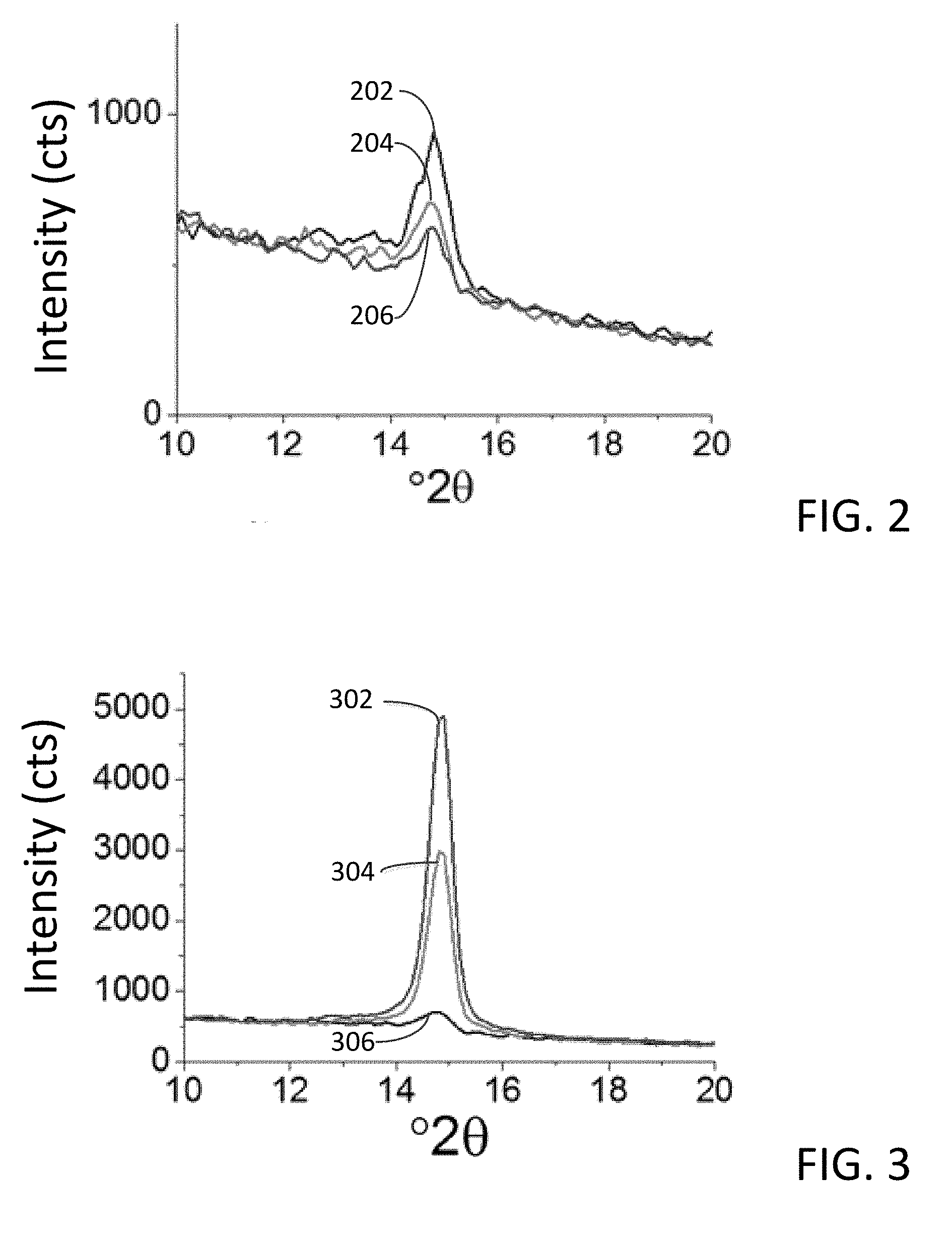
[0075] In some embodiments of the disclosure, the as-deposited metal chalcogenide thin film may be at least partially crystalline. For example, FIG. 2 illustrates grazing incidence x-ray diffraction (GIXRD) data for three (3) non-limiting examples of tin disulfide thin films, deposited utilizing the atomic layer deposition methods disclosed within, employing tin (IV) acetate (Sn(OAc).sub.4) as the tin containing precursor and hydrogen sulfide (H.sub.2S) as the chalcogen containing precursor, at a deposition temperature of approximately 150.degree. C. The GIXRD data illustrated in FIG. 2 demonstrates tin disulfide thin films deposited with different Sn(OAc).sub.4 pulse periods, for example, the data labelled as 202 illustrates a tin disulfide thin film deposited with a Sn(OAc).sub.4 pulse period of 0.2 second, the data labelled as 204 illustrates a tin disulfide thin film deposited with a Sn(OAc).sub.4 pulse period of 1 second and the data labelled as 206 illustrates a tin disulfide thin film deposited with a Sn(OAc).sub.4 pulse period of 2 seconds. The peak in the GIXRD data for the three (3) tin disulfide thin film corresponds to the (001) crystallographic orientation. Therefore, in some embodiments of the disclosure, depositing a tin dichalcogenide thin film comprises depositing a tin disulfide with a predominant (001) crystallographic orientation.
[0076] FIG. 3 illustrates GIXRD data for three (3) non-limiting examples of tin disulfide thin films, deposited utilizing the atomic layer deposition methods disclosed within, employing tin (IV) acetate (Sn(OAc).sub.4) as the tin containing precursor and hydrogen sulfide (H.sub.2S) as the chalcogen containing precursor, at a deposition temperature of approximately 150.degree. C. The GIXRD data illustrated in FIG. 3 demonstrates tin disulfide thin films deposited with different H.sub.2S pulse periods, for example, the data labelled as 302 illustrates a tin disulfide film deposited with a H.sub.2S pulse period of 8 seconds, the data labelled as 304 illustrates a tin disulfide film deposited with a H.sub.2S pulse period of 4 seconds and the data labelled as 306 illustrates a tin disulfide film deposited with a H.sub.2S pulse period of 2 seconds. As demonstrated previously, the peak in the GIXRD data for the three (3) tin disulfide thin films corresponds to the (001) crystallographic orientation. In addition, the peak in the GIXRD increases in intensity with an increased H.sub.2S pulse period, demonstrating that the crystallinity of the tin disulfide thin film increases with increased H.sub.2S pulse time. Therefore, in some embodiments of the disclosure, the deposition of a tin disulfide thin film comprises pulsing the chalcogen containing precursor (e.g., H.sub.2S) for a time period greater than approximately 2 seconds, or greater than approximately 4 seconds, or even greater than approximately 8 seconds.
[0077] Although the as-deposited metal chalcogenide thin films may be at least partially crystalline, the crystallization of the metal chalcogenide thin films may proceed slowly during the deposition process, such that thinner films may be less crystalline than thicker films. This may be problematic when the metal chalcogenide thin films comprise a 2D material with a thickness of less than approximately 10 nanometers. Therefore, in some embodiments of the disclosure, the as-deposited metal chalcogenide thin films may be subjected to a post-deposition annealing process to improve the crystallinity of the metal chalcogenide thin films. For example, in some embodiments, the method of depositing the metal chalcogenide may further comprise a post-deposition annealing of the metal chalcogenide at a temperature between approximately 150.degree. C. and approximately 300.degree. C. In some embodiments, annealing of the metal chalcogenide may comprise heating the metal chalcogenide to a temperature of approximately less than 800.degree. C., or approximately less than 600.degree. C., or approximately less than 500.degree. C., or even approximately less than 400.degree. C. In some embodiments, the post-deposition annealing of the metal chalcogenide thin film may be performed in an atmosphere comprising a chalcogen, for example, the post-deposition annealing process may be performed in an ambient comprising a chalcogenide compound, for example sulfur compounds, such as, a hydrogen sulfide (H.sub.2S) atmosphere. In some embodiments, the post-deposition annealing of the metal chalcogenide thin film may be performed for a time period of less than 1 hour, or less than 30 minutes, or less than 15 minutes, or even less than 5 minutes. In some embodiments, the post-deposition annealing of the metal chalcogenide thin film, such as a tin dichalcogenide thin film, may be performed in an atmosphere not comprising chalcogens, such as S, Se, or Te, for example, in inert gas ambient such as N.sub.2, or noble gas, such as Ar or He, or in hydrogen containing ambient such as H.sub.2 or H.sub.2/N.sub.2 ambient.
[0078] Thin films comprising a metal chalcogenide film, such as, for example, tin disulfide thin films, deposited according to some of the embodiments described herein may be continuous thin films comprising a 2D material. In some embodiments the thin films comprising a metal chalcogenide film deposited according to some of the embodiments described herein may be continuous at a thickness below about 100 nm, below about 60 nm, below about 50 nm, below about 40 nm, below about 30 nm, below about 25 nm, or below about 20 nm or below about 15 nm or below about 10 nm or below about 5 nm or lower. The continuity referred to herein can be physically continuity or electrical continuity. In some embodiments the thickness at which a film may be physically continuous may not be the same as the thickness at which a film is electrically continuous, and the thickness at which a film may be electrically continuous may not be the same as the thickness at which a film is physically continuous.
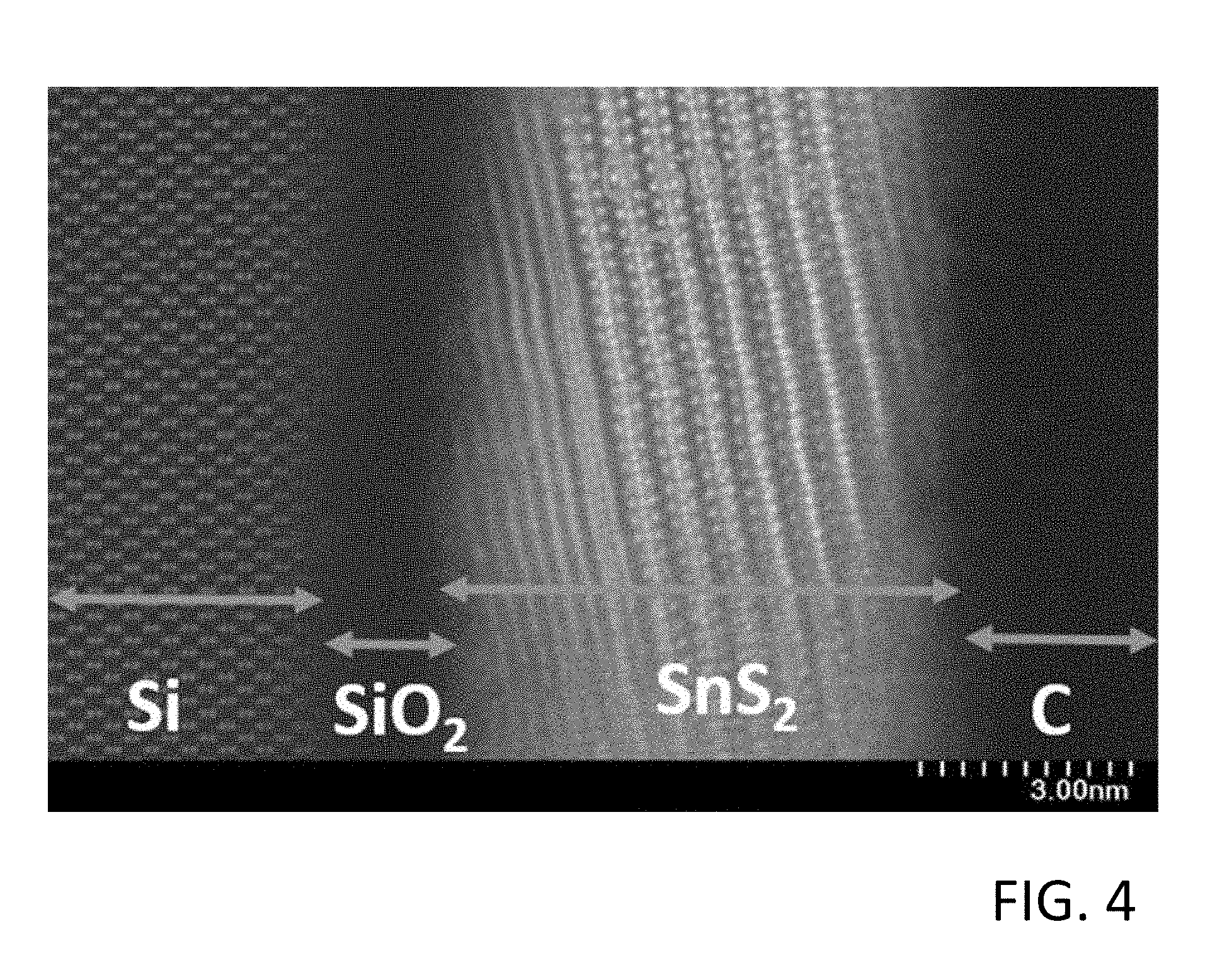
[0079] FIG. 4 illustrates a cross sectional high-angle annular dark-field scanning transmission electron microscopy (HAADF-STEM) image of structure comprising a tin dichalcogenide 2D material deposited according to the embodiments of the disclosure. The HAADF-STEM image illustrates a structure comprising a silicon substrate, silicon dioxide (SiO.sub.2) disposed over the silicon substrate and a tin disulfide 2D material disposed over the silicon dioxide. The structure may further comprise a layer of carbon (C) disposed over the tin disulfide, wherein the layer of carbon (C) is applied as part of the imaging procedure. FIG. 4 clearly demonstrates a crystalline tin disulfide (SnS.sub.2) 2D material, with a 2D crystal structure, and a thickness of approximately less than 8 nanometers.
[0080] The tin dichalcogenide thin film deposited by the embodiments of the disclosure may comprise tin disulfide and may take the form SnS.sub.x wherein x may range from approximately 0.75 to approximately 2.8, or wherein x may range from approximately 0.8 to approximately 2.5, or wherein x may range from 0.9 to approximately 2.3, or alternatively wherein x may range from approximately 0.95 to approximately 2.2. The elemental composition ranges for SnS.sub.x may comprise Sn from about 30 atomic % to about 60 atomic %, or from about 35 atomic % to about 55 atomic %, or even from about 40 atomic % to about 50 atomic %. Alternatively the elemental composition ranges for SnS.sub.x may comprise S from about 25 atomic % to about 75 atomic %, or S from about 30 atomic % to about 60 atomic %, or even S from about 35 atomic % to about 55 atomic %.
[0081] In some embodiments of the disclosure, the phase of the metal chalcogenide, for example, tin disulfide, may be determined utilizing Raman spectroscopy. For example, FIG. 5 illustrates the Raman spectra, measured with a 325 nanometer laser, of a 7 nanometer thick tin disulfide thin film after annealing at a temperature of 250.degree. C. The Raman spectrum illustrated in FIG. 5 clearly shows a peak in intensity at 313 cm' corresponding to the SnS.sub.2 peak. No peaks from other SnS phases, such as SnS or Sn.sub.2S.sub.3, were detected in the measurement. Therefore, in some embodiments of the disclosure, depositing a tin dichalcogenide comprises depositing a tin disulfide thin film with a stoichiometry given by SnS.sub.2.
[0082] In additional embodiments, the SnS may comprise less than about 20 atomic % oxygen, less than about 10 atomic % oxygen, less than about 5 atomic % oxygen, or even less than about 2 atomic % oxygen. In further embodiments, the SnS may comprise less than about 10 atomic % hydrogen, or less than about 5 atomic % of hydrogen, or less than about 2 atomic % of hydrogen, or even less than about 1 atomic % of hydrogen. In yet further embodiments, the SnS may comprise less than about 10 atomic % carbon, or less than about 5 atomic % carbon, or less than about 2 atomic % carbon, or less than about 1 atomic % of carbon, or even less than about 0.5 atomic % carbon. In the embodiments outlined herein, the atomic concentration of an element may be determined utilizing Rutherford backscattering (RBS).
[0083] In some embodiments of the disclosure, the metal chalcogenide thin film may be deposited on a three-dimensional structure. In some embodiments, the step coverage of the metal chalcogenide thin film may be equal to or greater than about 50%, greater than about 80%, greater than about 90%, about 95%, about 98%, or about 99% or greater in structures having aspect ratios (height/width) of more than about 2, more than about 5, more than about 10, more than about 25, more than about 50, or even more than about 100.
[0084] In some embodiments a metal chalcogenide thin film, such as a tin dichalcogenide thin film comprising, tin and a chalcogen deposited according to some of the embodiments described herein may be crystalline or polycrystalline. In some embodiments, a metal chalcogenide thin film deposited according to some of the embodiments described herein may have a thickness from about 20 nm to about 100 nm. In some embodiments, a metal chalcogenide thin film deposited according to some of the embodiments described herein may have a thickness from about 20 nm to about 60 nm. In some embodiments, a metal chalcogenide thin film deposited according to some of the embodiments described herein may have a thickness greater than about 20, greater than about 30 nm, greater than about 40 nm, greater than about 50 nm, greater than about 60 nm, greater than about 100 nm, greater than about 250 nm, greater than about 500 nm, or greater. In some embodiments a metal chalcogenide thin film deposited according to some of the embodiments described herein may have a thickness of less than about 50 nm, less than about 30 nm, less than about 20 nm, less than about 15 nm, less than about 10 nm, less than about 5 nm, less than about 3 nm, less than about 2 nm, or even less than about 1 nm.
[0085] In some embodiments a metal chalcogenide thin film, such as a tin or germanium dichalcogenide thin film deposited according to some of the embodiments described herein may have a thickness of equal or less than about 10 monolayers of metal chalcogenide material, equal or less than about 7 monolayers of metal chalcogenide material, equal or less than about 5 monolayers of metal chalcogenide material, equal or less than about 4 monolayers of metal chalcogenide material, equal or less than about 3 monolayers of metal chalcogenide material, equal or less than about 2 monolayers of metal chalcogenide material, or even equal or less than about 1 monolayer of metal chalcogenide material.
[0086] The metal chalcogenide films deposited by the cyclical deposition processes disclosed herein may be utilized in a variety of contexts, such as in the formation of semiconductor device structures. One of skill in the art will recognize that the processes described herein are applicable to many contexts, including the fabrication of transistors.
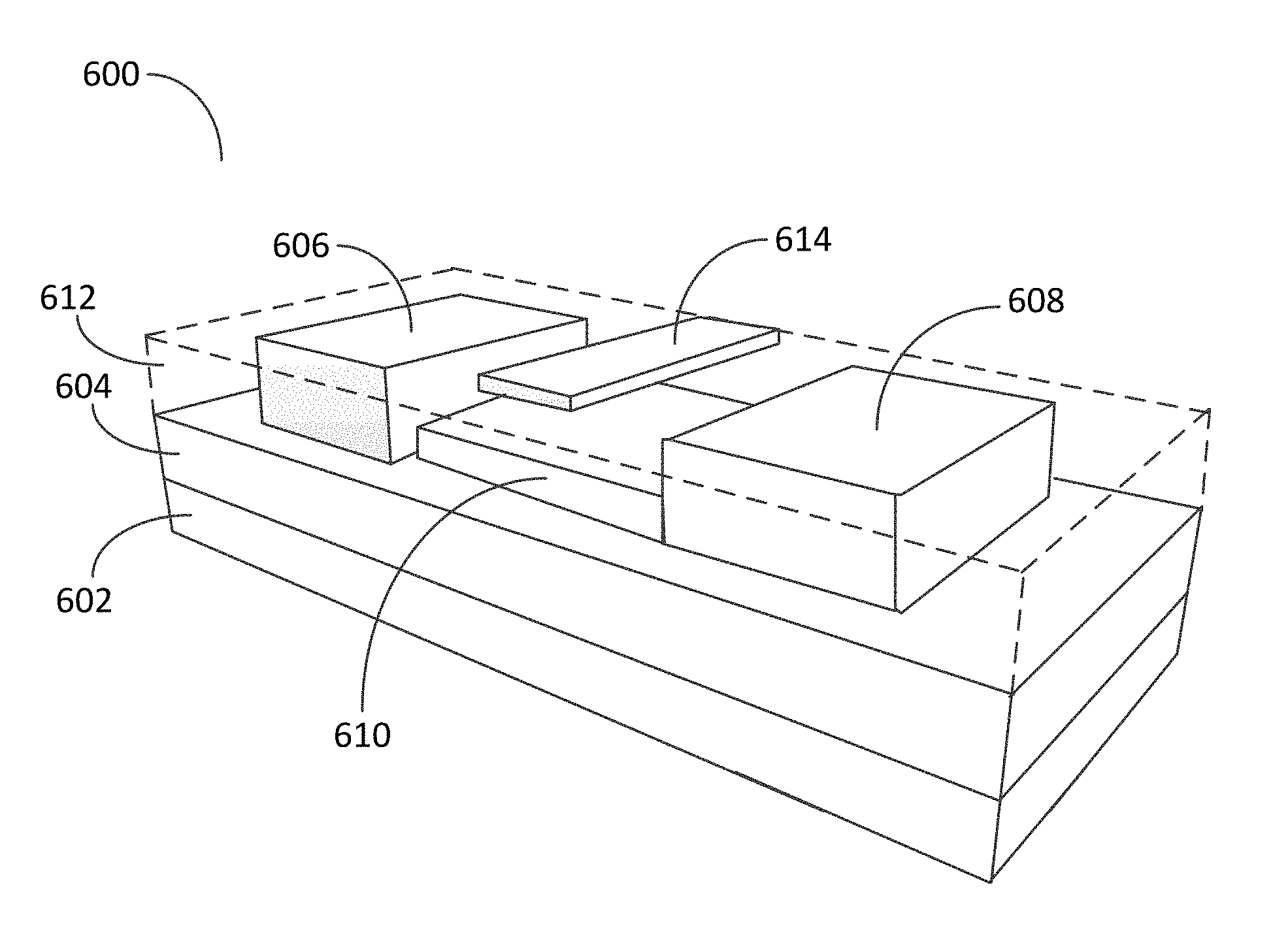
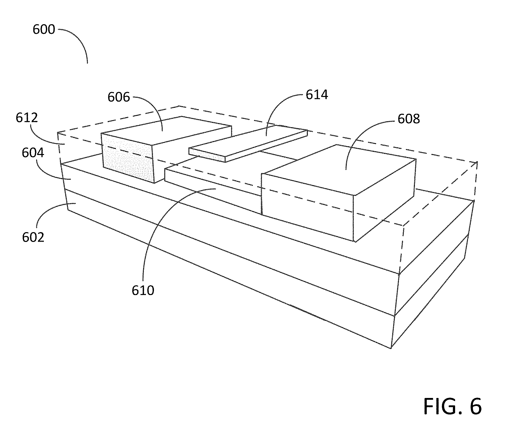
[0087] As a non-limiting example, and with reference to FIG. 6, a semiconductor device structure 600 may comprise a field effect transistor (FET) which may include a silicon substrate 602 and a silicon dioxide (SiO.sub.2) layer 604 disposed over the silicon substrate 602. The semiconductor device structure 600 may further comprise a source region 606 and a drain region 608. Disposed between the source and drain regions is a thin film of a metal chalcogenide 610 deposited according to the embodiments of the disclosure. The thin film of metal chalcogenide may comprise a thin layer of tin disulfide and may consist of the channel region of the FET structure. In some embodiments of the disclosure the thin layer of tin disulfide may have thickness of less than 10 nm, or less than 5 nm, or even less than 1 nm. The semiconductor device structure 600 may further comprise a gate dielectric layer 612 disposed over the thin film of tin disulfide, wherein the gate dielectric layer 612 may comprise hafnium dioxide (HfO.sub.2). The semiconductor device structure 600 may further comprise a gate electrode 614 disposed over the thin layer of tin disulfide 610.
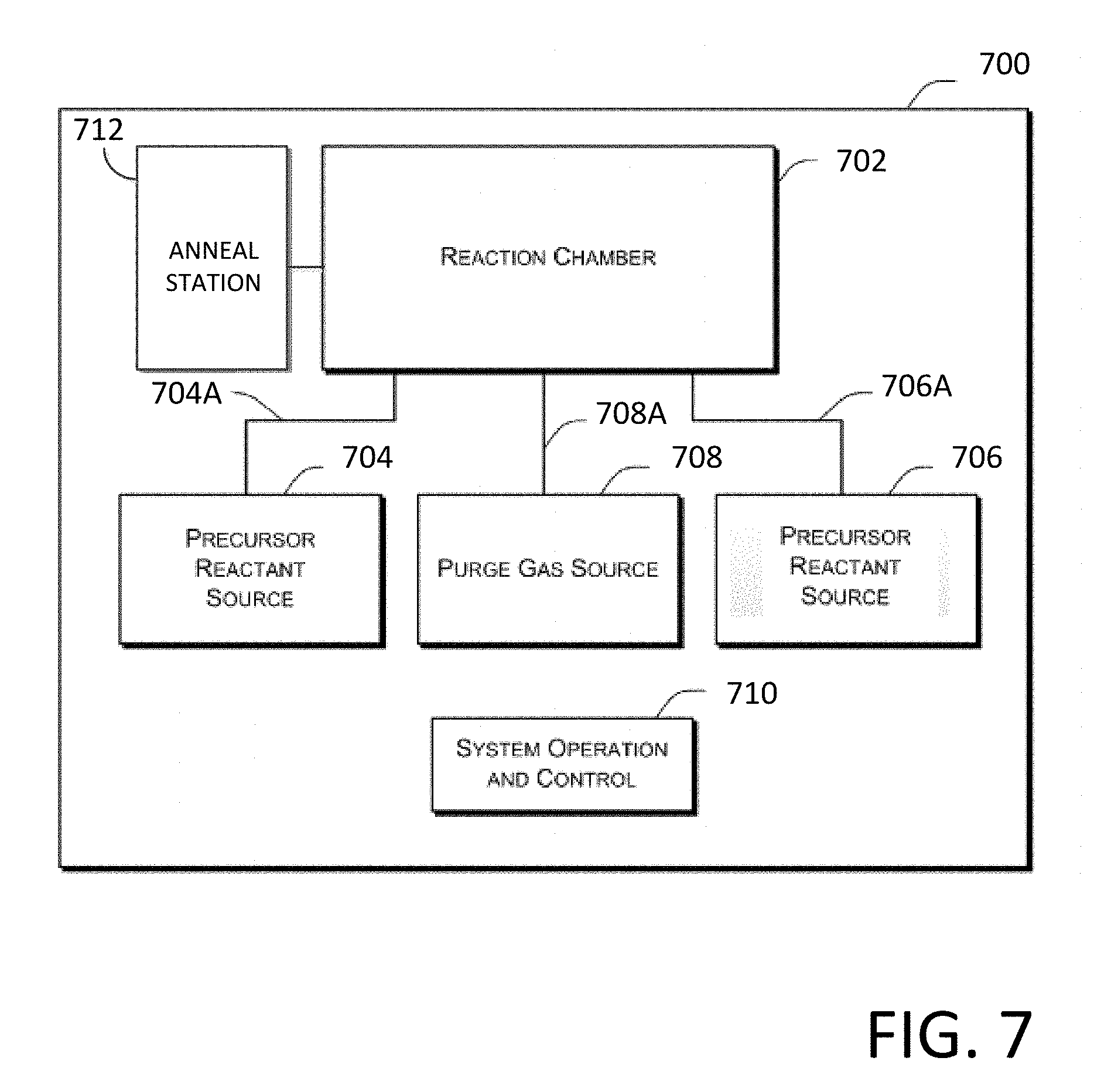
[0088] Embodiments of the disclosure may also include a reaction system configured for forming the metal chalcogenide films of the present disclosure. In more detail, FIG. 7 schematically illustrates a reaction system 700 including a reaction chamber 702 that further includes mechanism for retaining a substrate (not shown) under predetermined pressure, temperature, and ambient conditions, and for selectively exposing the substrate to various gases. A precursor reactant source 704 may be coupled by conduits or other appropriate means 704A to the reaction chamber 702, and may further couple to a manifold, valve control system, mass flow control system, or mechanism to control a gaseous precursor originating from the precursor reactant source 704. A precursor (not shown) supplied by the precursor reactant source 704, the reactant (not shown), may be liquid or solid under room temperature and standard atmospheric pressure conditions. Such a precursor may be vaporized within a reactant source vacuum vessel, which may be maintained at or above a vaporizing temperature within a precursor source chamber. In such embodiments, the vaporized precursor may be transported with a carrier gas (e.g., an inactive or inert gas) and then fed into the reaction chamber 702 through conduit 704A. In other embodiments, the precursor may be a vapor under standard conditions. In such embodiments, the precursor does not need to be vaporized and may not require a carrier gas. For example, in one embodiment the precursor may be stored in a gas cylinder. The reaction system 700 may also include additional precursor reactant sources, such precursor reactant source 706 which may also be coupled to the reaction chamber by conduits 706A as described above.
[0089] A purge gas source 708 may also be coupled to the reaction chamber 702 via conduits 708A, and selectively supplies various inert or noble gases to the reaction chamber 702 to assist with the removal of precursor gas or waste gasses from the reaction chamber. The various inert or noble gasses that may be supplied may originate from a solid, liquid or stored gaseous form.
[0090] The reaction system 700 of FIG. 7, may also optionally comprise anneal station 712, wherein the metal chalcogenide may be undergo a post-growth anneal process. In some embodiments, a post-growth anneal process may be carried out in the reaction chamber 702, whereas in some embodiments the metal chalcogenide thin film may be transferred (e.g., under a controlled atmosphere) to an anneal station 712, wherein the post-growth annealing process may be performed under a desired gaseous environment.
[0091] The reaction system 700 of FIG. 7, may also comprise a system operation and control mechanism 710 that provides electronic circuitry and mechanical components to selectively operate valves, manifolds, pumps and other equipment included in the reaction system 700. Such circuitry and components operate to introduce precursors, purge gasses from the respective precursor sources 704, 706 and purge gas source 708. The system operation and control mechanism 710 also controls timing of gas pulse sequences, temperature of the substrate and reaction chamber, and pressure of the reaction chamber and various other operations necessary to provide proper operation of the reaction system 700. The operation and control mechanism 710 can include control software and electrically or pneumatically controlled valves to control flow of precursors, reactants and purge gasses into and out of the reaction chamber 702. The control system can include modules such as a software or hardware component, e.g., a FPGA or ASIC, which performs certain tasks. A module can advantageously be configured to reside on the addressable storage medium of the control system and be configured to execute one or more processes.
[0092] Those of skill in the relevant arts appreciate that other configurations of the present reaction system are possible, including different number and kind of precursor reactant sources and purge gas sources. Further, such persons will also appreciate that there are many arrangements of valves, conduits, precursor sources, purge gas sources that may be used to accomplish the goal of selectively feeding gasses into reaction chamber 702. Further, as a schematic representation of a reaction system, many components have been omitted for simplicity of illustration, and such components may include, for example, various valves, manifolds, purifiers, heaters, containers, vents, and/or bypasses.
[0093] The example embodiments of the disclosure described above do not limit the scope of the invention, since these embodiments are merely examples of the embodiments of the invention, which is defined by the appended claims and their legal equivalents. Any equivalent embodiments are intended to be within the scope of this invention. Indeed, various modifications of the disclosure, in addition to those shown and described herein, such as alternative useful combination of the elements described, may become apparent to those skilled in the art from the description. Such modifications and embodiments are also intended to fall within the scope of the appended claims.
* * * * *
D00000
D00001
D00002
D00003
D00004
D00005
D00006
XML
uspto.report is an independent third-party trademark research tool that is not affiliated, endorsed, or sponsored by the United States Patent and Trademark Office (USPTO) or any other governmental organization. The information provided by uspto.report is based on publicly available data at the time of writing and is intended for informational purposes only.
While we strive to provide accurate and up-to-date information, we do not guarantee the accuracy, completeness, reliability, or suitability of the information displayed on this site. The use of this site is at your own risk. Any reliance you place on such information is therefore strictly at your own risk.
All official trademark data, including owner information, should be verified by visiting the official USPTO website at www.uspto.gov. This site is not intended to replace professional legal advice and should not be used as a substitute for consulting with a legal professional who is knowledgeable about trademark law.