Circuits And Methods For Slew Rate Control Of Switched Capacitor Regulators
Li; Thomas ; et al.
U.S. patent application number 15/903974 was filed with the patent office on 2019-08-29 for circuits and methods for slew rate control of switched capacitor regulators. The applicant listed for this patent is Lion Semiconductor Inc.. Invention is credited to Thomas Li, Zhipeng Li, Hans Meyvaert, Alberto Puggelli.
| Application Number | 20190265743 15/903974 |
| Document ID | / |
| Family ID | 67684489 |
| Filed Date | 2019-08-29 |

| United States Patent Application | 20190265743 |
| Kind Code | A1 |
| Li; Thomas ; et al. | August 29, 2019 |
CIRCUITS AND METHODS FOR SLEW RATE CONTROL OF SWITCHED CAPACITOR REGULATORS
Abstract
Circuits comprising: a first capacitor(C1); a first switch(S1) having a first side coupled to a VIN and a second side coupled to a first side of C1; a second switch(S2) having a first side coupled to the second side of S1; a third switch(S3) having a first side coupled to a second side of S2 and a second side coupled to a second side of C1; a fourth switch(S4) having a first side coupled to a second side of S3 and a second side coupled to a V.sub.SUPPLY, wherein: in a first state, S1 and S3 are off, and S2 and S4 are on; in a second state, S1 and S3 are on, and S2 and S4 are off; and at least one of a control of S1, a control of S2, a control of S3, and a control of S4 is coupled to a time-varying-slew-rate signal.
| Inventors: | Li; Thomas; (Mountain View, CA) ; Li; Zhipeng; (Fremont, CA) ; Puggelli; Alberto; (Burlingame, CA) ; Meyvaert; Hans; (Oakland, CA) | ||||||||||
| Applicant: |
|
||||||||||
|---|---|---|---|---|---|---|---|---|---|---|---|
| Family ID: | 67684489 | ||||||||||
| Appl. No.: | 15/903974 | ||||||||||
| Filed: | February 23, 2018 |
| Current U.S. Class: | 1/1 |
| Current CPC Class: | G05F 3/16 20130101; H02M 3/07 20130101; H02M 2001/0029 20130101 |
| International Class: | G05F 3/16 20060101 G05F003/16; H02M 3/07 20060101 H02M003/07 |
Claims
1. A circuit for a switched capacitor regulator, comprising: a first capacitor having a first side and a second side; a first switch having a first side coupled to an input voltage, a second side coupled to the first side of the first capacitor, and a control; a second switch having a first side coupled to the second side of the first switch, a second side, and a control; a third switch having a first side coupled to the second side of the second switch, a second side coupled to the second side of the first capacitor, and a control; a fourth switch having a first side coupled to the second side of the third switch, a second side coupled to a supply voltage, and a control, wherein in a first state: the first switch is off; the second switch is on, the third switch is off, and the fourth switch is on, wherein in a second state: the first switch is on, the second switch is off, the third switch is on, and the fourth switch is off, wherein at least one of the control of the first switch, the control of the second switch, the control of the third switch, and the control of the fourth switch is coupled to a control signal that is controlled to repeatedly transition between a low state a high state with a constant predetermined frequency, and wherein the control signal is controlled to have a slew rate during each transition between the low state to the high state that causes a switch corresponding to the at least one control to have an on-state resistance determined by the slew rate that regulates a voltage at the second side of the second switch while switching between the low state and the high state at the constant predetermined frequency.
2. The circuit of claim 1, wherein the first switch is a PMOS FET, and the control of the first switch is a gate of the PMOS FET.
3. The circuit of claim 1, wherein the second switch is an NMOS FET, and the control of the second switch is a gate of the NMOS FET.
4. The circuit of claim 1, wherein the third switch is a PMOS FET, and the control of the third switch is a gate of the PMOS FET.
5. The circuit of claim 1, wherein the fourth switch is an NMOS FET, and the control of the fourth switch is a gate of the NMOS FET.
6. The circuit of claim 1, wherein the supply voltage is ground.
7. The circuit of claim 1, further comprising a second capacitor having a first side coupled to the second side of the second capacitor switch and a second side coupled to the supply voltage.
8. The circuit of claim 1, further comprising a variable capacitance having a first side coupled to one of the control of the first switch, the control of the second switch, the control of the third switch, and the control of the fourth switch.
9. The circuit of claim 8, wherein the variable capacitance is a bank of switched capacitors.
10. The circuit of claim 8, wherein the variable capacitance is a varactor.
11. The circuit of claim 1, further comprising: a variable current source having an output; and a third capacitor having a first side coupled to the supply voltage and having a second side coupled to the output of the variable current source and one of the control of the first switch, the control of the second switch, the control of the third switch, and the control of the fourth switch.
Description
BACKGROUND
[0001] Switched capacitor regulators are a well-known class of regulator that can be used to regulate voltage or current. In many existing switched capacitor regulators, a network of switches in the regulators switch the regulators between two states. The output voltage or the output current of such regulators can be regulated by adjusting the frequency at which the regulators switch between states. However, changing the switching frequency can be prohibitive in electronic devices that are sensitive to electromagnetic interference (EMI). For example, mobile phones have strict specifications on EMI because too much EMI can affect call quality and wireless data transfer, and mobile phone engineers often need to adjust the operating frequency of various chips to prevent them from interfering with the key communication signals to ensure call quality does not degrade. To meet the strict EMI specification, the SC regulator might need to operate at a predictable, single switching frequency. In this case, the SC regulator cannot adjust the switching frequency to regulate the output voltage.
[0002] Accordingly, new mechanisms for regulating the output of switched capacitor regulators are desirable.
SUMMARY
[0003] In accordance with some embodiments, circuits and methods for slew rate control of switched capacitor regulators are provided. More particularly, in some embodiments, circuits for a switched capacitor regulator are provided, the circuits comprising: a first capacitor having a first side and a second side; a first switch having a first side coupled to an input voltage, a second side coupled to the first side of the first capacitor, and a control; a second switch having a first side coupled to the second side of the first switch, a second side, and a control; a third switch having a first side coupled to the second side of the second switch, a second side coupled to the second side of the first capacitor, and a control; a fourth switch having a first side coupled to the second side of the third switch, a second side coupled to a supply voltage, and a control, wherein in a first state: the first switch is off; the second switch is on, the third switch is off, and the fourth switch is on, wherein in a second state: the first switch is on, the second switch is off, the third switch is on, and the fourth switch is off, and wherein at least one of the control of the first switch, the control of the second switch, the control of the third switch, and the control of the fourth switch is coupled to a control signal having a slew rate that varies over time.
[0004] Still more particularly, in some of these embodiments, the first switch is a PMOS FET, and the control of the first switch is a gate of the PMOS FET.
[0005] Still more particularly, in some of these embodiments, the second switch is an NMOS FET, and the control of the second switch is a gate of the NMOS FET.
[0006] Still more particularly, in some of these embodiments, the third switch is a PMOS FET, and the control of the third switch is a gate of the PMOS FET.
[0007] Still more particularly, in some of these embodiments, the fourth switch is an NMOS FET, and the control of the fourth switch is a gate of the NMOS FET.
[0008] Still more particularly, in some of these embodiments, the supply voltage is ground.
[0009] Still more particularly, in some of these embodiments, the circuits further comprise a second capacitor having a first side coupled to the second side of the second capacitor and a second side coupled to the supply voltage.
[0010] Still more particularly, in some of these embodiments, the circuits further comprise a variable capacitance having a first side coupled to one of the control of the first switch, the control of the second switch, the control of the third switch, and the control of the fourth switch. Even still more particularly, in some of these embodiments, the variable capacitance is a bank of switched capacitors. Even still more particularly, in some of these embodiments, the variable capacitance is a varactor.
[0011] Still more particularly, in some of these embodiments, the circuits further comprise a variable current source having an output; third capacitor having a first side coupled to the supply voltage and having a second side coupled to the output of the variable current source and one of the control of the first switch, the control of the second switch, the control of the third switch, and the control of the fourth switch.
BRIEF DESCRIPTION OF THE DRAWINGS
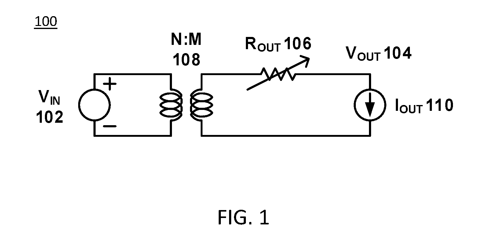
[0012] FIG. 1 is an example of a model of an N:M switched capacitor (SC) regulator in accordance with some embodiments.
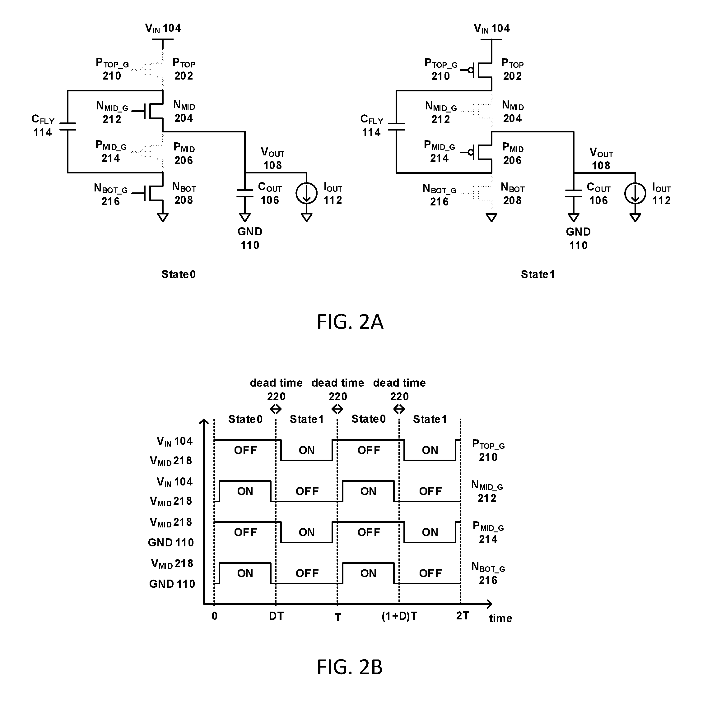
[0013] FIG. 2A is an example of a 2:1 SC regulator in accordance with some embodiments.
[0014] FIG. 2B illustrates examples of waveforms for four gates of the 2:1 SC regulator of FIG. 2A in accordance with some embodiments.
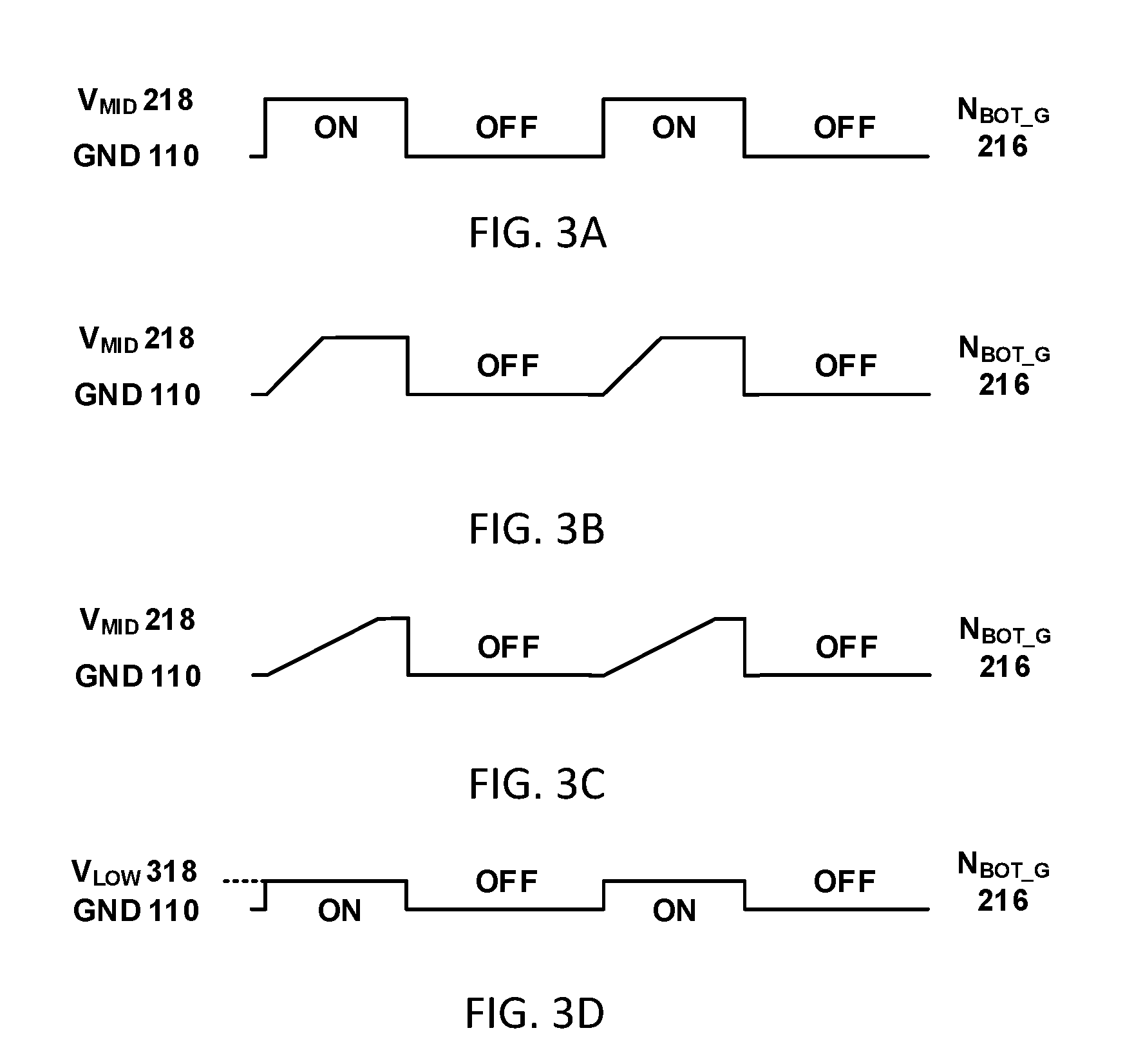
[0015] FIGS. 3A-3C illustrate examples of gate drive waveforms with different slew rates in accordance with some embodiments.
[0016] FIG. 3D illustrates an example of a way to adjust the effective VGS by adjusting the supply voltage of the drivers that generate the gate driver signals in accordance with some embodiments.
[0017] FIG. 4A is an example of first circuit for changing slew rate in accordance with some embodiments.
[0018] FIG. 4B is an example of a second circuit for changing slew rate in accordance with some embodiments.
DETAILED DESCRIPTION
[0019] In accordance with some embodiments, mechanisms for regulating the output of switched capacitor regulators using variable slew rates on the control signals of power switches are provided.
[0020] FIG. 1 illustrates an example 100 of a model of an N:M switched capacitor (SC) regulator in accordance with some embodiments. For example, if N is 2 and M is 1, the SC regulator model 100 describes a 2:1 SC regulator. The input voltage VIN 102 is multiplied by the ratio M/N 108, which is followed by the output resistor R.sub.OUT 106. V.sub.OUT=M.times.V.sub.IN/N-R.sub.OUT.times.I.sub.OUT. R.sub.OUT 106 can be adjusted by changing the switching frequency of the SC regulator, but that can be prohibitive due to EMI reasons in certain applications. R.sub.OUT 106 can also be adjusted by changing the effective resistance of power switches. One way to do this is to change the slew rate of the gate driver signals going to the power switches.
[0021] FIG. 2A illustrates an example of a 2:1 SC regulator 102 in accordance with some embodiments. As shown, regulator 102 includes four power switches P.sub.TOP 202, N.sub.MID 204, P.sub.MID 206, and N.sub.BOT 208. Any suitable components can be used to implement these switches in some embodiments. For example, in some embodiments, P.sub.TOP 202 and P.sub.MID 206 can be PMOS FET power switches, while N.sub.MID 204 and N.sub.BOT 208 can be NMOS FET power switches.
[0022] During operation, these switches can turn on and off to cause the regulator to transition between State 0 and State 1 to regulate V.sub.OUT 108 to be close to 1/2 of V.sub.IN 104. These switches can be controlled by four gate signals P.sub.TOP_G 210, N.sub.MID_G 212, P.sub.MID_G 214, and N.sub.BOT_G 216 of the four power switches P.sub.TOP 202, N.sub.MID 204, P.sub.MID 206, and N.sub.BOT 208. The gate signals drive a respective gate of P.sub.TOP 202, N.sub.MID 204, P.sub.MID 206, and N.sub.BOT 208 to turn them on or off.
[0023] As shown in FIG. 2A, in state 0, P.sub.TOP 202 and P.sub.MID 206 are turned off (as indicated by dashed lines) and N.sub.MID 204 and N.sub.BOT 208 are turned on. In state 1, P.sub.TOP 202 and P.sub.MID 206 are turned on, while N.sub.MID 204 and N.sub.BOT 208 are turned off (as indicated by dashed lines). As illustrated in FIG. 2A, in state 0: a first side of C.sub.FLY 114 can be coupled by N.sub.MID 204 to a first side of a decoupling capacitor C.sub.OUT 106 and an output that outputs V.sub.OUT 108; and a second side of C.sub.FLY 114 can be coupled by M.sub.BOT 208 to ground. In state 1: the first side of C.sub.FLY 114 can be coupled by P.sub.TOP 202 to V.sub.IN 104; and the second side of C.sub.FLY 114 can be coupled by P.sub.MID 206 to the first side of decoupling capacitor C.sub.OUT 106 and the output that outputs V.sub.OUT 108. In both state 0 and state 1, a second node of C.sub.OUT 106 can be coupled to ground 110 in some embodiments.
[0024] FIG. 2B illustrates example waveforms for the four gates P.sub.TOP_G 210, N.sub.MID_G 212, P.sub.MID_G 214, and N.sub.BOT_G 216 of the four power switches P.sub.TOP 202, N.sub.MID 204, P.sub.MID 206, and N.sub.BOT 208, respectively, that can be used in some embodiments. V.sub.MID 218 can be connected to V.sub.OUT 108 or can be supplied by a separate voltage regulator that generates a voltage close to 1/2 of the input voltage V.sub.IN 104, in some embodiments.
[0025] As illustrated in FIG. 2B, P.sub.TOP_G 210 and P.sub.MID_G 214 can share the same signal, and N.sub.MID_G 212 and N.sub.BOT_G 216 can share the same signal, in some embodiments. In some embodiments, there can be a dead time 220 between the turn off time of N.sub.MID_G 212 and turn on time of P.sub.TOP_G 210 to provide enough margin to guarantee that both switches are never turned on at the same time, which can lead to malfunction of the SC regulator. Any suitable duration dead time can be used in some embodiments.
[0026] Even when a power switch is on, there is a non-zero on-state resistance due to non-ideal parasitic resistance. The on-state resistance of power switches can be adjusted to adjust ROUT to regulate an SC regulator. The on-state resistance of a MOSFET is roughly inversely proportional to (V.sub.GS-V.sub.th) (V.sub.GS is the gate to source voltage of a MOSFET, and V.sub.th is the threshold voltage of a MOSFET), so changing the average value of V.sub.GS during on-state of the switch is one way to change on-state resistance.
[0027] This can be done by adjusting the slew rate of gate drive signals. FIGS. 3A-3C illustrate examples of gate drive waveforms with different slew rates that can be as gate drive signals. By using different waveforms, one can control the on-state resistance. FIG. 3A has the highest effective V.sub.GS, or highest average value of V.sub.GS during on-state, which leads to lowest on-state resistance on NBOT 208. FIG. 3B has lower effective V.sub.GS and FIG. 3C has the lowest effective V.sub.GS. Decreasing slew rate on NBOT_G 216 can lead to lower effective V.sub.GS and lower R.sub.OUT in some embodiments. This can be applied to switches other than N.sub.BOT 208 as well in some embodiments.
[0028] As illustrated in FIG. 3D, in some embodiments, another way to adjust the effective V.sub.GS can be to adjust the supply voltage of the drivers that generate the gate driver signals (e.g., N.sub.BOT_G 216). In FIG. 3D, N.sub.BOT_G 216 switches between GND 110 and V.sub.LOW 318, which is a variable voltage level that is lower voltage than V.sub.MID 218. The drawback of this method is it requires an additional voltage regulator to generate the variable voltage V.sub.LOW 318. V.sub.LOW 318 can be any value between GND 110 and V.sub.MID 218. The lower the V.sub.LOW 318 voltage, the higher the on-state resistance of N.sub.BOT 208. By adjusting the on-state resistance of N.sub.BOT 208, the regulator can regulate the output voltage or output current.
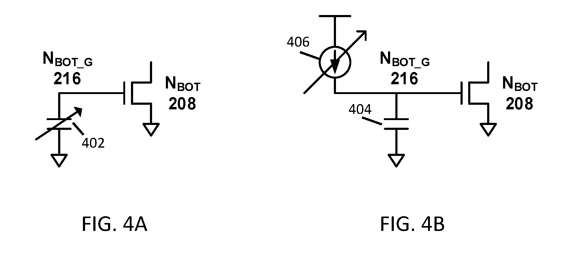
[0029] In contrast, changing slew rate can be done with very simple circuits. Two examples of circuits that can be used to change slew rate in accordance with some embodiments are illustrated in FIGS. 4A-4B. As illustrated in FIG. 4A, there can be an adjustable capacitance 402, which can be an array of capacitors that are connected or disconnected, or a varactor, on the gate of N.sub.BOT 208. More capacitance results in lower slew rate of N.sub.BOT_G 216 and lower effective V.sub.GS during on-state of N.sub.BOT 208. As illustrated in FIG. 4B, another example is to have a variable current source 406 (which can be implemented in any suitable manner, such as, e.g., a MOSFET with adjustable gate voltage) providing charge to a capacitor 404 connected to the gate of N.sub.BOT 208. As the current increases, the slew rate on N.sub.BOT_G 216 increases. Both variable current and variable capacitance can be used in some embodiments to allow for a wide range of slew rate on N.sub.BOT_G 216.
[0030] Similar circuits can be applied to other power switches including P.sub.TOP 202, N.sub.MID 204, and P.sub.MID 206.
[0031] Although the invention has been described and illustrated in the foregoing illustrative embodiments, it is understood that the present disclosure has been made only by way of example, and that numerous changes in the details of implementation of the invention can be made without departing from the spirit and scope of the invention, which is limited only by the claims that follow. Features of the disclosed embodiments can be combined and rearranged in various ways.
* * * * *
D00000
D00001
D00002
D00003
D00004
XML
uspto.report is an independent third-party trademark research tool that is not affiliated, endorsed, or sponsored by the United States Patent and Trademark Office (USPTO) or any other governmental organization. The information provided by uspto.report is based on publicly available data at the time of writing and is intended for informational purposes only.
While we strive to provide accurate and up-to-date information, we do not guarantee the accuracy, completeness, reliability, or suitability of the information displayed on this site. The use of this site is at your own risk. Any reliance you place on such information is therefore strictly at your own risk.
All official trademark data, including owner information, should be verified by visiting the official USPTO website at www.uspto.gov. This site is not intended to replace professional legal advice and should not be used as a substitute for consulting with a legal professional who is knowledgeable about trademark law.