Apparatus For Detecting Or Monitoring For A Chemical Precursor In A High Temperature Environment
Shugrue; John ; et al.
U.S. patent application number 16/242852 was filed with the patent office on 2019-08-29 for apparatus for detecting or monitoring for a chemical precursor in a high temperature environment. The applicant listed for this patent is ASM IP Holding B.V.. Invention is credited to John Shugrue, Carl White.
| Application Number | 20190264324 16/242852 |
| Document ID | / |
| Family ID | 67684352 |
| Filed Date | 2019-08-29 |


| United States Patent Application | 20190264324 |
| Kind Code | A1 |
| Shugrue; John ; et al. | August 29, 2019 |
APPARATUS FOR DETECTING OR MONITORING FOR A CHEMICAL PRECURSOR IN A HIGH TEMPERATURE ENVIRONMENT
Abstract
An apparatus and method are disclosed for monitoring and/or detecting concentrations of a chemical precursor in a reaction chamber. The apparatus and method have an advantage of operating in a high temperature environment. An optical emissions spectrometer (OES) is coupled to a gas source, such as a solid source vessel, in order to monitor or detect an output of the chemical precursor to the reaction chamber. Alternatively, a small sample of precursor can be periodically monitored flowing into the OES and into a vacuum pump, thus bypassing the reaction chamber.
| Inventors: | Shugrue; John; (Phoenix, AZ) ; White; Carl; (Gilbert, AZ) | ||||||||||
| Applicant: |
|
||||||||||
|---|---|---|---|---|---|---|---|---|---|---|---|
| Family ID: | 67684352 | ||||||||||
| Appl. No.: | 16/242852 | ||||||||||
| Filed: | January 8, 2019 |
Related U.S. Patent Documents
| Application Number | Filing Date | Patent Number | ||
|---|---|---|---|---|
| 62634793 | Feb 23, 2018 | |||
| Current U.S. Class: | 1/1 |
| Current CPC Class: | G01N 21/15 20130101; C23C 16/448 20130101; C23C 16/505 20130101; H01J 2237/24485 20130101; G01J 3/443 20130101; G01N 21/68 20130101; C23C 16/455 20130101; H01J 37/32972 20130101; C23C 16/45536 20130101; C23C 16/45544 20130101; G01N 2201/08 20130101; H01J 2237/24507 20130101; H01J 37/3244 20130101 |
| International Class: | C23C 16/455 20060101 C23C016/455; H01J 37/32 20060101 H01J037/32; C23C 16/505 20060101 C23C016/505; G01N 21/68 20060101 G01N021/68; G01J 3/443 20060101 G01J003/443 |
Claims
1. A device for monitoring a concentration of a gas source comprising: a solid source vessel, the solid source vessel containing a solid precursor and sublimating the solid precursor into a first gas precursor; a gas line coupled to the solid source vessel, the gas line configured to move a first portion of the first gas precursor into a reaction chamber and move a second portion of the first gas precursor into a sampling port; a RF source coupled to the sampling port, the RF source ionizing the first gas precursor; an optical emissions spectrometer coupled to the RF source, the optical emissions spectrometer configured to obtain a light spectrum of the ionized first gas precursor; and an exhaust pump coupled to the RF source and configured to exhaust the ionized first gas precursor; wherein a concentration of the ionized first gas precursor is determined based on the light spectrum.
2. The device of claim 1, further comprising a heater to heat a part of the gas line connected to the RF source.
3. The device of claim 1, further comprising a plurality of valves to control a flow of the first gas precursor from the solid source vessel.
4. The device of claim 1, wherein the RF source comprises at least one of: an inductively coupled plasma source; a capacitively coupled plasma source; a microwave source; or a hot filament gas ionizer.
5. The device of claim 1, further comprising a flow restrictor disposed between the RF source and the exhaust pump.
6. The device of claim 1, further comprising an optical fiber coupling the RF source to the optical emissions spectrometer.
7. The device of claim 6, wherein the optical fiber comprises: a light transmission section; a purge gas channel; an outer sheath; a wide view fiber optic attached to the light transmission section; and a purge nozzle attached to the outer sheath.
8. The device of claim 1, further comprising a heated vacuum enclosure to hold at least the solid source vessel.
9. The device of claim 8, further comprising a flow restrictor within the heated vacuum enclosure.
10. The device of claim 1, further comprising an inert gas source configured to provide an inert carrier gas for the first gas precursor.
11. An apparatus for depositing a film on a semiconductor wafer comprising: a first reaction chamber configured to hold a first semiconductor wafer; a first gas source configured to provide a first gas precursor to the first reaction chamber; a second gas source configured to provide a second gas precursor to the first reaction chamber, the second gas source comprising a first solid source vessel, the first solid source vessel containing a solid precursor and sublimating the solid precursor into the second gas precursor; a first gas line coupled to the first solid source vessel, the first gas line configured to move a first portion of the second gas precursor into the first reaction chamber and move a second portion of the second gas precursor into a first sampling port; a RF source coupled to the first sampling port, the RF source ionizing the second gas precursor; an optical emissions spectrometer coupled to the RF source, the optical emissions spectrometer configured to obtain a light spectrum of the ionized second gas precursor; and an exhaust pump coupled to the RF source and configured to exhaust the ionized second gas precursor; wherein a concentration of the ionized second gas precursor is determined based on the light spectrum.
12. The apparatus of claim 11, wherein the RF source comprises at least one of: an inductively coupled plasma source; a capacitively coupled plasma source; a microwave source; or a hot filament gas ionizer.
13. The apparatus of claim 11, further comprising a flow restrictor disposed between the RF source and the exhaust pump.
14. The apparatus of claim 11, further comprising an optical fiber coupling the RF source to the optical emissions spectrometer.
15. The apparatus of claim 14, wherein the optical fiber comprises: a light transmission section; a purge gas channel; an outer sheath; a wide view fiber optic attached to the light transmission section; and a purge nozzle attached to the outer sheath.
16. The apparatus of claim 11, further comprising: a second reaction chamber configured to hold a second semiconductor wafer; a third gas source configured to provide a third gas precursor to the second reaction chamber; a fourth gas source configured to provide a fourth gas precursor to the second reaction chamber, the second gas source comprising a second solid source vessel, the second solid source vessel containing a second solid precursor and sublimating the second solid precursor into the fourth gas precursor; and a second gas line coupled to the second solid source vessel, the second gas line configured to move a first portion of the fourth gas precursor into the second reaction chamber and move a second portion of the fourth gas precursor into a second sampling port; wherein the RF source is coupled to the second sampling port and ionizes the fourth gas precursor; and wherein the optical emissions spectrometer couples to the RF source and is configured to obtain a light spectrum of the ionized fourth gas precursor.
17. The apparatus of claim 11, further comprising a first inert gas source configured to provide an inert carrier gas for the first gas precursor.
18. The apparatus of claim 11, further comprising a heated vacuum enclosure to hold at least the first solid source vessel.
Description
CROSS-REFERENCE TO RELATED APPLICATION
[0001] This application claims the benefit of U.S. Provisional Application No. 62/634,793 entitled "APPARATUS FOR DETECTING OR MONITORING FOR A CHEMICAL PRECURSOR IN A HIGH TEMPERATURE ENVIRONMENT" and filed on Feb. 23, 2018, the disclosure of which is hereby incorporated herein for reference.
FIELD OF INVENTION
[0002] The present disclosure generally relates to an apparatus for forming a film on a semiconductor substrate. Specifically, the present disclosure relates to a chemical source for the apparatus and detecting or monitoring a concentration of a gas provided by the chemical source.
BACKGROUND OF THE DISCLOSURE
[0003] Chemical Vapor Deposition (CVD) and Atomic Layer Deposition (ALD) are both processes used to form a film on a semiconductor substrate disposed within a reaction chamber. The processes may involve flow of a first gas onto the substrate and flow of a second gas onto the substrate, such that the first gas reacts with the second gas in order to form a film having a particular chemical composition on the semiconductor substrate.
[0004] The chemistries used for these processes generally are kept in particular conditions in order to ensure proper film formation and to avoid any defects or clogging issues. Defects may occur due to condensation of heated chemistries along a gas pathway to the reaction chamber. The condensation of the heated chemistries may lead to a chemical reaction within the gas pathway prior to reaching the reaction chamber, leading to adverse particle formation on the film formed within the reaction chamber.
[0005] In addition, clogging may occur within the gas pathways due to the condensation. Clogging may result in shutting down operation of the reaction chamber in order to clear the gas pathways, as well as exacerbate the particle formation that adversely affects the film formed in the chamber. In addition, changes to process conditions may affect the deposition onto the wafer; for example, a change in temperature or pressure may lead to shifts in non-uniformities as it relates to film properties. These process shifts may lead to non-uniformities in thickness or concentration of the film, potentially resulting in scrapped wafers.
[0006] Prior art approaches to monitor concentrations of chemistries have been limited to temperatures less than 60-80.degree. C. At these temperatures, condensation of gaseous precursors may occur, leading to the above described problems. An example of such a setup is described in the article entitled "Effluent Stream Monitoring of An Al2O3 Atomic Layer Deposition Process Using Optical Emission Spectroscopy," by John P. Loo (available at http://www.lightwindcorp.com/uploads/6/2/8/7/6282375/ald_effluent_monitor- ing_.pdf).
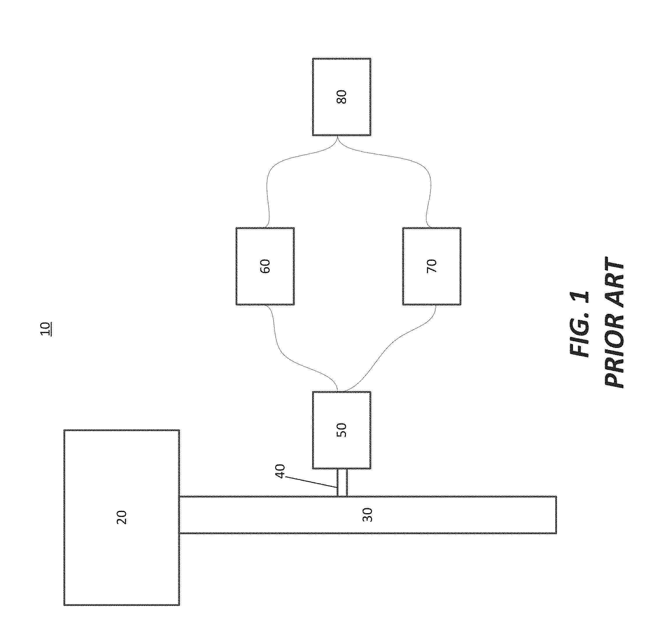
[0007] FIG. 1 illustrates a prior art optical emissions spectroscopy setup 10 in an exhaust foreline. The optical emissions spectroscopy setup 10 comprises a reaction chamber 20, an exhaust foreline 30, a sampler 40, an optical emission source 50, an optical emission spectrometer 60, an RF supply 70, and a processor 80. Exhaust from the reaction chamber 20 travels through the exhaust foreline 30. The sampler 40 may take a portion of the exhaust in the exhaust foreline 30 and pass it through the optical emission source 50, which may be an inductively coupled plasma source. The optical spectrometer 60 and the RF supply 70 are able to take readings of a spectrum generated in the optical emission source 50 and provide a reading to the processor 80.
[0008] As a result, an apparatus and method to monitor concentrations of chemical precursors in a high temperature environment is desired.
BRIEF DESCRIPTION OF THE DRAWING FIGURES
[0009] While the specification concludes with claims particularly pointing out and distinctly claiming what are regarded as embodiments of the invention, the advantages of embodiments of the disclosure may be more readily ascertained from the description of certain examples of the embodiments of the disclosure when read in conjunction with the accompanying drawing, in which:
[0010] FIG. 1 illustrates a prior art optical emissions spectroscopy approach;
[0011] FIG. 2 illustrates an exemplary reaction chamber in accordance with at least one embodiment of the invention;
[0012] FIG. 3 illustrates a spectroscopy apparatus in accordance with at least one embodiment of the invention;
[0013] FIGS. 4A-4C illustrate a spectroscopy apparatus in accordance with at least one embodiment of the invention;
[0014] FIGS. 5A-5B illustrate an optical fiber apparatus in accordance with at least one embodiment of the invention; and
[0015] FIG. 6 illustrates a multiple reaction chamber setup in accordance with at least one embodiment of the invention.
[0016] It will be appreciated that elements in the figures are illustrated for simplicity and clarity and have not necessarily been drawn to scale. For example, the dimensions of some of the elements in the figures may be exaggerated relative to other elements to help improve understanding of illustrated embodiments of the present disclosure.
DETAILED DESCRIPTION OF EXEMPLARY EMBODIMENTS
[0017] Although certain embodiments and examples are disclosed below, it will be understood by those in the art that the invention extends beyond the specifically disclosed embodiments and/or uses of the invention and obvious modifications and equivalents thereof. Thus, it is intended that the scope of the invention disclosed should not be limited by the particular disclosed embodiments described below.
[0018] As used herein, the term "substrate" may refer to any underlying material or materials that may be used, or upon which, a device, a circuit or a film may be formed.
[0019] As used herein, the term "chemical vapor deposition" (CVD) may refer to any process wherein a substrate is exposed to one or more volatile precursors, which react and/or decompose on a substrate surface to produce a desired deposition.
[0020] As used herein, the term "atomic layer deposition" (ALD) may refer to a vapor deposition process in which deposition cycles, preferably a plurality of consecutive deposition cycles, are conducted in a process chamber. Typically, during each cycle the precursor is chemisorbed to a deposition surface (e.g., a substrate surface or a previously deposited underlying surface such as material from a previous ALD cycle), forming a monolayer or sub-monolayer that does not readily react with additional precursor (i.e., a self-limiting reaction). Thereafter, if necessary, a reactant (e.g., another precursor or reaction gas) may subsequently be introduced into the process chamber for use in converting the chemisorbed precursor to the desired material on the deposition surface. Typically, this reactant is capable of further reaction with the precursor. Further, purging steps may also be utilized during each cycle to remove excess precursor from the process chamber and/or remove excess reactant and/or reaction byproducts from the process chamber after conversion of the chemisorbed precursor. Further, the term "atomic layer deposition," as used herein, is also meant to include processes designated by related terms such as, "chemical vapor atomic layer deposition", "atomic layer epitaxy" (ALE), molecular beam epitaxy (MBE), gas source MBE, or organometallic MBE, and chemical beam epitaxy when performed with alternating pulses of precursor composition(s), reactive gas, and purge (e.g., inert carrier) gas.
[0021] In the specification, it will be understood that the term "on" or "over" may be used to describe a relative location relationship, another element or layer may be directly on the mentioned layer, or another layer (an intermediate layer) or element may be intervened therebetween, or a layer may be disposed on a mentioned layer but not completely cover a surface of the mentioned layer. Therefore, unless the term "directly" is separately used, the term "on" or "over" will be construed to be a relative concept. Similarly to this, it will be understood the term "under," "underlying," or "below" will be construed to be relative concepts.
[0022] Embodiments of the invention are directed to an apparatus and a method for monitoring or detecting a concentration of a chemical precursor that enters a reaction chamber. Importance of such monitoring is due to the fact that such CVD and ALD processes may require strict chemical concentrations in order to form films of a particular composition and quality. It may be necessary to verify in real-time that an appropriate amount of the chemical precursor is being delivered with each pulse or flow. By such detection or monitoring, a variation in delivery of precursor to the wafers can be detected, and potentially, this could avoid scrapping of wafers.
[0023] An Optical Emission Spectrometer (OES) may be used to verify the proper amount of chemical precursor. An example of an OES may include the L3 "Smart" Chemical Monitoring System manufactured by Lightwind Corporation. Other OES may include the Sensor X system manufactured by Pivotal Systems. An OES determines measures intensities along a wavelength spectrum of a light emanating from a specimen. In this case, the specimen may be the chemical precursor. The intensities may represent an amount of chemical precursor flowing through the OES.
[0024] FIG. 2 illustrates a reaction system 100 in accordance with at least one embodiment of the invention. The reaction system 100 comprises a reaction chamber 110; a gas source 120 for providing a gas reactant; a showerhead 130 for distributing a gas; and a substrate holder 140 for holding a substrate 150 to be processed. The reaction system 100 also includes a passageway 160 through which the gas reactant flows from the gas source 120 to the showerhead 130. The gas source 120 may provide a plasma gas source in at least one embodiment, or may provide a gas generated by a solid source precursor.
[0025] Prior approaches with implementing an OES into a reaction system have not incorporated the OES directly between a solid source vessel and the reaction chamber. Embodiments in accordance with the invention may perform a real-time monitoring of a vapor delivered from a solid source vessel into a reactor. Real-time monitoring may be to monitor a gas phase emission spectrum of each wafer, preferably after a few first pulses when stability may be reached. Alternative embodiments may not measure an absolute concentration, but just detect for the presence of a particular chemistry and perform a precursor sampling. With this arrangement, an acceptable range of operation may be determined, with anything outside an error range resulting in fault detection.
[0026] In addition, embodiments may measure or detect concentrations of particular chemistries at the solid source vessel or on a foreline of gas going towards the reaction chamber. Particular embodiments may allow for obtaining better signals and readings compared to other embodiments of the invention. A better signal may be obtained, but via an apparatus setup that may reduce the amount of precursor that enters into the reaction chamber, resulting in a higher cost to operate the reaction chamber.
[0027] Additional benefits obtained by embodiments of the invention may include an ability to match processes within more than one reaction chamber. An OES may be used to ensure that each reaction chamber is receiving an acceptably matching does of chemistry. The OES may also determine if certain chemicals used in the film formation are present in an acceptable and repeatable amount for given process conditions.
[0028] FIG. 3 illustrates the gas source 120 in accordance with at least one embodiment of the invention. The gas source 120 may be configured to perform a real-time concentration monitoring. The gas source 120 comprises a heated vacuum enclosure 200, an RF source 220, an optical emissions spectrometer 230, an exhaust pump 240, a flow restrictor 250, a valve 260A, a gas line 270A, a plurality of heaters 280A-280B, and an optical fiber 300. The heated vacuum enclosure 200 comprises a solid source vessel 210, a plurality of valves 260B-260C, and a gas line 270B.
[0029] The solid source vessel 210 may hold a solid precursor and convert it into a gaseous precursor. The solid source vessel 210 may be a vessel described in U.S. patent application Ser. No. 15/283,120, entitled "Reactant Vaporizer and Related Systems and Methods" and filed on Sep. 30, 2016, or in U.S. patent application Ser. No. 15/585,540, entitled "Reactant Vaporizer and Related Systems and Methods" and filed on May 3, 2017, both of which are incorporated by reference.
[0030] The gaseous precursor then travels from the solid source vessel 210 through a valve 260C, and then can either go along a gas line 270B to the passageway 160 or to the RF source 220 via a valve 260B. The majority of the gaseous precursor goes to the passageway 160 and subsequently the reaction chamber 110, where it will reach the surface of the wafer 150.
[0031] Of the gas that does not go to the reaction chamber 110, the RF source 220 takes the draw of gaseous precursor and ionizes it. The RF source may be an inductively coupled plasma source, a capacitively coupled plasma source, a microwave source, or a hot filament gas ionizer; an example of such an RF source may include an ICP, manufactured by Lightwand, for example. The optical emissions spectrometer 230 is able to obtain a light spectrum of the ionized gaseous precursor in the RF source 220 through the optical fiber 300. The optical emissions spectrometer 230 may then monitor desired wavelengths in order to determine whether there is an acceptable amount of gaseous precursor. The ionized gaseous precursor in the RF source 220 then passes through the flow restrictor 250 and a valve 260A to the exhaust pump 240 along a gas line 270A.
[0032] In addition, the flow restrictor 250 may prevent an excess of gaseous precursor from being sent to the exhaust pump 240, and thus, result in more efficient use of the gaseous precursor. The flow restrictor 250 may comprise a control orifice, a needle valve, or a fixed or variable restrictor, for example. The heaters 280A-280B would provide heat to a gaseous precursor diverted from the solid source vessel 210 to the RF source 220, as well as the precursor traveling along the gas line 270B. The heating of the gaseous precursor primarily avoids condensation of the gaseous precursor.
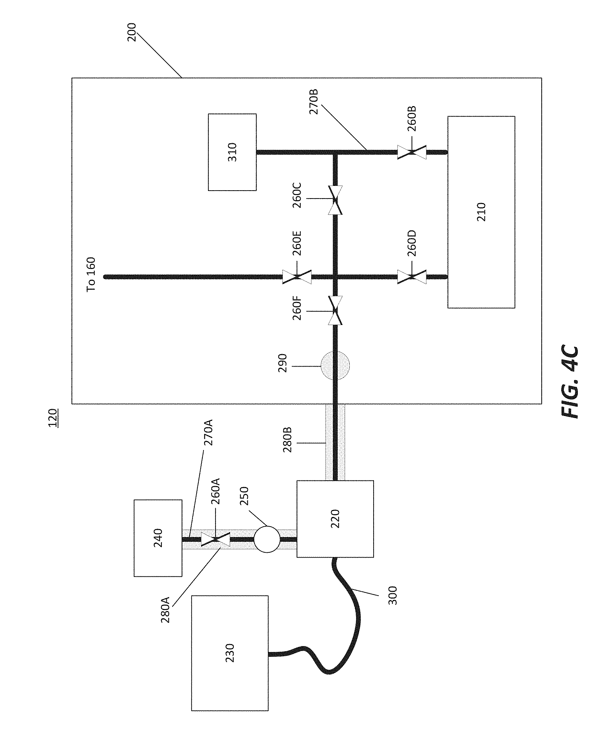
[0033] FIG. 4A illustrates a gas source 120 in accordance with at least one embodiment of the invention. The embodiment of the invention allows for flow of gas through the RF source rather than diffusion of gas into the RF source; this may result in a stronger spectrometer reading. The gas source 120 may detect a presence of a chemical in a setup allowing for precursor sampling. The gas source 120 comprises a heated vacuum enclosure 200. The heated vacuum enclosure 200 comprises a solid source vessel 210, a plurality of valves 260B-260F, a gas line 270B, a flow restrictor 290, and an inert gas source 310. Gas from the inert gas source 310 travels in the gas line 270a through the valve 260b into the solid source vessel 210, where it carries a gaseous precursor formed from a solid precursor. The resulting gaseous precursor travels through the valves 260D-260E and may either go to the reaction chamber 160 or be sampled by going through valve 260F and the flow restrictor 290. The valve 260C serves as a bypass valve in isolating the solid source vessel 210.
[0034] The gas source 120 also comprises an RF source 220, an optical emissions spectrometer 230, an exhaust pump 240, a flow restrictor 250, a valve 260A, a plurality of heaters 280A-280B, a gas line 270b, and an optical fiber 300. The heater 280A heats exhaust gas within the gas line 270A, while the heater 280B heats the portion of the gas line 270B disposed between the vacuum enclosure 200 and the RF source.
[0035] FIG. 4B illustrates a gas source 120 in accordance with at least one embodiment of the invention. The gas source 120 is similar to that illustrated in FIG. 4A as it also is capable of performing a periodic detection of a chemical concentration. A gas line 270c is split from a gas line 270b, while a heater 280 heats the gas line outside of a vacuum enclosure 200 up to an RF source 220 and a valve 260a.
[0036] An optical fiber 300 may obtain a light spectrum signal from the RF source 220 and provide it to an optical emissions spectrometer 230. The arrangement of the RF source 220 and the optical fiber 300 may avoid deposition of a film on a window attached to the optical fiber 300. In addition, build-up of a precursor may be avoided within a vacuum exhaust that travels through the valve 260a and a pump 240 along the gas line 270c.
[0037] FIG. 4C illustrates a gas source 120 in accordance with at least one embodiment of the invention. The gas source 120 is similar to that illustrated in FIG. 4A, with the main difference in that a valve 260F is disposed between a gas line having a valve 260D and a valve 260E, while in FIG. 4A, the valve 260F is disposed in the gas line after the valve 260E. In other words, the valve 260F is upstream of the valve 260E in FIG. 4C, while it is disposed downstream of the valve 260E in FIG. 4A. The embodiment illustrated in FIG. 4C may sample the gaseous precursor between processing of wafers or front opening unified pods (FOUPs) rather than real time monitoring.
[0038] FIGS. 5A-5B illustrate an optical fiber 300 in accordance with at least one embodiment of the invention. FIG. 5A illustrates an end view of the optical fiber 300, while FIG. 5B illustrates a cross-sectional view of the optical fiber 300. The optical fiber 300 comprises a light transmission section 310, a purge gas channel 320, and a high-temperature outer sheath 330. The optical fiber 300 also comprises a wide view fiber optic 340 attached to the light transmission section 310 and a purge nozzle 350 attached to the high-temperature outer sheath 330. The purge nozzle 350, along with a purge gas traveling through the purge gas channel 320, may allow for reducing or minimizing build-up of a film formed on the wide view fiber optic 340. The optical fiber 300 may be useful for monitoring within a foreline disposed proximate to a gas source.
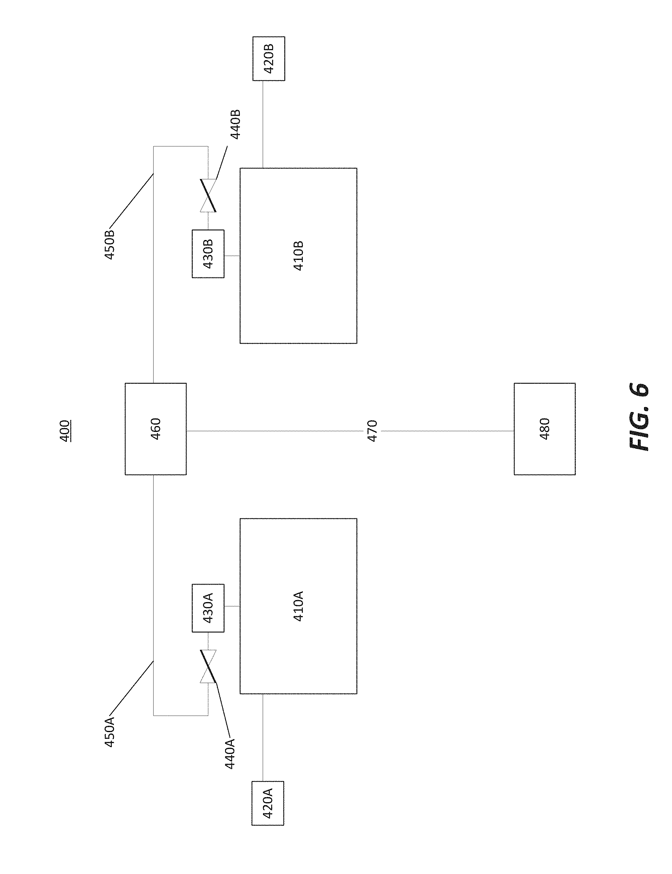
[0039] FIG. 6 illustrates a multiple reaction chamber setup 400 in accordance with at least one embodiment of the invention. The multiple reaction chamber setup 400 allows for a matching of the process in multiple chambers, and comprises: a first reaction chamber 410A, a second reaction chamber 410B, a first gas source 420A, a second gas source 420B, a first sampling port 430A, a second sampling port 430B, a first valve 440A, a second valve 440B, a first gas line 450A, a second gas line 450B, a RF source/OES device 460, an exhaust line 470, and an exhaust pump 480.
[0040] The first gas source 420A and the second gas source 420B may be configured to provide a same gaseous precursor to the first reaction chamber 410A and the second reaction chamber 410B. The first sampling port 430A may be configured to sample a gas within the first reaction chamber 410A. In an alternative embodiment, the first sampling port 430A may be configured to be between the first gas source 420A and the first reaction chamber 410A. Similarly, the second sampling port 430B may be configured to sample a gas within the second reaction chamber 410B. In an alternative embodiment, the second sampling port 430B may be configured to be between the second gas source 420B and the second reaction chamber 410B.
[0041] The first valve 440A and the second valve 440B may be configured to restrict the amount of gas that leaves the first reaction chamber 410A and the second reaction chamber 410B and into the first gas line 450A and the second gas line 450B, respectively. The first valve 440A and the second valve 440B may comprise a needle valve, a fixed flow restrictor, or a variable flow restrictor, for example. The first gas line 450A and the second gas line 450B may feed into the RF source/OES 460; in an alternative embodiment, there may be separate RF source/OES setups for each of the first gas line 450A and the second gas line 450B. The RF source/OES 460 may perform a gas ionization and a spectrometry reading in a manner described previously on the gaseous precursor, before sending the gas to the exhaust pump 480 via the exhaust line 470.
[0042] The example embodiments of the disclosure described above do not limit the scope of the invention, since these embodiments are merely examples of the embodiments of the invention, which is defined by the appended claims and their legal equivalents. Any equivalent embodiments are intended to be within the scope of this invention. Indeed, various modifications of the disclosure, in addition to those shown and described herein, such as alternative useful combination of the elements described, may become apparent to those skilled in the art from the description. Such modifications and embodiments are also intended to fall within the scope of the appended claims.
* * * * *
References
D00000
D00001
D00002
D00003
D00004
D00005
D00006
D00007
D00008
XML
uspto.report is an independent third-party trademark research tool that is not affiliated, endorsed, or sponsored by the United States Patent and Trademark Office (USPTO) or any other governmental organization. The information provided by uspto.report is based on publicly available data at the time of writing and is intended for informational purposes only.
While we strive to provide accurate and up-to-date information, we do not guarantee the accuracy, completeness, reliability, or suitability of the information displayed on this site. The use of this site is at your own risk. Any reliance you place on such information is therefore strictly at your own risk.
All official trademark data, including owner information, should be verified by visiting the official USPTO website at www.uspto.gov. This site is not intended to replace professional legal advice and should not be used as a substitute for consulting with a legal professional who is knowledgeable about trademark law.