Systems And Methods Of Dislocation Filtering For Layer Transfer
Kim; Jeehwan ; et al.
U.S. patent application number 16/348125 was filed with the patent office on 2019-08-22 for systems and methods of dislocation filtering for layer transfer. This patent application is currently assigned to Massachusetts Institute of Technology. The applicant listed for this patent is Massachusetts Institute of Technology. Invention is credited to Jeehwan Kim, Kyusang Lee.
| Application Number | 20190259608 16/348125 |
| Document ID | / |
| Family ID | 62110590 |
| Filed Date | 2019-08-22 |


| United States Patent Application | 20190259608 |
| Kind Code | A1 |
| Kim; Jeehwan ; et al. | August 22, 2019 |
SYSTEMS AND METHODS OF DISLOCATION FILTERING FOR LAYER TRANSFER
Abstract
A method of manufacturing a semiconductor device includes forming a first epitaxial layer on a first substrate. The first substrate includes a first semiconductor material having a first lattice constant and the first epitaxial layer includes a second semiconductor material having a second lattice constant different from the first lattice constant. The method also includes disposing a graphene layer on the first epitaxial layer and forming a second epitaxial layer comprising the second semiconductor material on the graphene layer. This method can increase the substrate reusability, increase the release rate of functional layers, and realize precise control of release thickness.
| Inventors: | Kim; Jeehwan; (Camdridge, MA) ; Lee; Kyusang; (Camdridge, MA) | ||||||||||
| Applicant: |
|
||||||||||
|---|---|---|---|---|---|---|---|---|---|---|---|
| Assignee: | Massachusetts Institute of
Technology Camdridge MA |
||||||||||
| Family ID: | 62110590 | ||||||||||
| Appl. No.: | 16/348125 | ||||||||||
| Filed: | November 8, 2017 | ||||||||||
| PCT Filed: | November 8, 2017 | ||||||||||
| PCT NO: | PCT/US2017/060568 | ||||||||||
| 371 Date: | May 7, 2019 |
Related U.S. Patent Documents
| Application Number | Filing Date | Patent Number | ||
|---|---|---|---|---|
| 62418964 | Nov 8, 2016 | |||
| Current U.S. Class: | 1/1 |
| Current CPC Class: | H01L 21/02444 20130101; H01L 21/02458 20130101; H01L 21/02485 20130101; H01L 21/02392 20130101; H01L 21/683 20130101; H01L 21/02502 20130101; H01L 21/02389 20130101; H01L 21/02455 20130101; H01L 21/762 20130101 |
| International Class: | H01L 21/02 20060101 H01L021/02; H01L 21/683 20060101 H01L021/683; H01L 21/762 20060101 H01L021/762 |
Claims
1. A method of manufacturing a semiconductor device, the method comprising: forming a first epitaxial layer on a first substrate, the first substrate comprising a first semiconductor material having a first lattice constant and the first epitaxial layer comprising a second semiconductor material having a second lattice constant different from the first lattice constant; disposing a graphene layer on the first epitaxial layer; and forming a second epitaxial layer comprising the second semiconductor material on the graphene layer.
2. The method of claim 1, wherein the first substrate comprises GaN and the first epitaxial layer comprises InGaN.
3. The method of claim 1, wherein the first substrate comprises GaAs and the first epitaxial layer comprises InGaP.
4. The method of claim 1, wherein the first substrate comprises InP and the first epitaxial layer comprises InGaAs.
5. The method of claim 1, wherein disposing the graphene layer comprises: forming the graphene layer on a second substrate; transferring the graphene layer from the second substrate to the first epitaxial layer.
6. The method of claim 5, wherein the second substrate comprises silicon carbide and the graphene layer comprises a single-crystalline graphene layer.
7. The method of claim 5, wherein the second substrate comprises a copper foil and the graphene layer comprises a poly-crystalline graphene layer.
8. The method of claim 1, further comprising: transferring the second epitaxial layer to a host substrate.
9. The method of claim 8, wherein transferring the second epitaxial layer comprises exfoliating the second epitaxial layer from the graphene layer and disposing the second epitaxial layer on the host substrate.
10. The method of claim 8, wherein transferring the second epitaxial layer comprises: forming a metal stressor on the second epitaxial layer; disposing a flexible tape on the metal stressor; and pulling the second epitaxial layer and the metal stressor off the graphene layer with the flexible tape.
11. The method of claim 8, further comprising: forming a third epitaxial layer comprising the second semiconductor material on the graphene layer after transferring the second epitaxy layer to the host substrate.
12. A semiconductor device formed by the method of claim 1.
13. A method of manufacturing a semiconductor device, the method comprising: disposing a graphene layer on a first substrate comprising a first semiconductor material having a first lattice constant; forming an epitaxial layer on the graphene layer, the epitaxial layer comprising a second semiconductor material having a second lattice constant different from the first lattice constant; and transferring the epitaxial layer to a host substrate.
14. The method of claim 13, wherein the graphene layer has a thickness substantially equal to or less than 1 nm.
15. The method of claim 13, wherein disposing graphene layer comprises: forming the graphene layer on a second substrate; transferring the graphene layer from the second substrate to the first substrate.
16. The method of claim 15, wherein the second substrate comprises silicon carbide and the graphene layer comprises a single-crystalline graphene layer.
17. The method of claim 15, wherein the second substrate comprises a copper foil and the graphene layer comprises a poly-crystalline graphene layer.
18. The method of claim 13, wherein transferring the epitaxial layer comprises: forming a metal stressor on the epitaxial layer; disposing a flexible tape on the metal stressor; and pulling the epitaxial layer and the metal stressor off the graphene layer with the flexible tape.
19. The method of claim 18, wherein the epitaxial layer is a first epitaxial layer and the method further comprises: forming a second epitaxial layer comprising the second semiconductor material on the graphene layer after transferring the first epitaxial layer to the host substrate.
20. A semiconductor device formed by the method of claim 13.
21. A method of manufacturing a semiconductor device, the method comprising: disposing a graphene layer on a first substrate comprising a first semiconductor material having a first lattice constant; forming a graded buffer layer on the graphene layer; forming a transfer handle layer on the graded buffer layer; and transferring the graded buffer layer to a host substrate using the transfer handle layer.
22. The method of claim 21, wherein the graded buffer layer comprises: a first buffer layer having a first lattice constant; and a second buffer layer disposed on the first buffer layer and having a second lattice constant different from the first lattice constant.
23. The method of claim 21, wherein the graded buffer layer comprises: a first buffer layer having a first lattice constant; a separation layer comprising graphene disposed on the first buffer layer; and a second buffer layer having a second lattice constant different from the first lattice constant.
24. The method of claim 21, wherein the graded buffer layer comprises: a plurality of buffer layers, an ith buffer layer in the plurality of buffer layers having a lattice constant a.sub.i and an (i+1)th buffer layer in the plurality of buffer layers having a lattice constant a.sub.i+1 greater than a.sub.i, where i is a positive integer; and a plurality of separation layers comprising graphene, an ith separation layer in the plurality of separation layers being disposed between the ith buffer layer and the (i+1)th buffer layer.
25. The method of claim 21, wherein the graded buffer layer is a first graded buffer layer and the method further comprises: forming a second graded buffer layer on the graphene layer after transferring the first graded buffer layer to the host substrate.
26. The method of claim 21, further comprising: removing the transfer handle layer to expose the graded buffer layer; and forming an epitaxial layer on the graded buffer layer.
Description
CROSS-REFERENCES TO RELATED APPLICATIONS
[0001] This application claims the priority benefit under 35 U.S.C. .sctn. 119(e) of U.S. Application No. 62/418,964, filed Nov. 8, 2016, entitled "DISLOCATION-FILTERING TECHNIQUE FOR GRAPHENE-BASED LAYER TRANSFER," which is hereby incorporated herein by reference in its entirety.
BACKGROUND
[0002] In advanced electronic and photonic technologies, devices are usually fabricated from functional semiconductors, such as III-N semiconductors, III-V semiconductors, II-VI semiconductors, and Ge. The lattice constants of these functional semiconductors typically do not match the lattice constants of silicon substrates. Lattice constant mismatch between a substrate and an epitaxial layer on the substrate can introduce strain into the epitaxial layer, thereby preventing epitaxial growth of thicker layers without defects. Therefore, non-silicon substrates are usually employed as seeds for epitaxial growth of most functional semiconductors. However, non-Si substrates with lattice constants matching those of functional materials can be costly and therefore limit the development of non-Si electronic/photonic devices.
[0003] One method to address the high cost of non-silicon substrates is the "layer-transfer" technique, in which functional device layers are grown on lattice-matched substrates and then removed and transferred to other substrates. The remaining lattice-matched substrates can then be reused to fabricate another device layer, thereby reducing the cost. To significantly reduce manufacturing costs, it can be desirable for a layer-transfer method to have the following properties: 1) substrate reusability; 2) a minimal substrate refurbishment step after the layer release; 3) a fast release rate; and 4) precise control of release thickness.
[0004] Conventional methods to remove and transfer a device layer from a lattice-matched substrate include chemical lift-off (also referred to as epitaxial lift-off or ELO), optical lift-off (also referred to as laser lift-off or LLO), and mechanical lift-off (also referred to as controlled spalling). Unfortunately, none of these methods has all four desired properties at the same time.
[0005] The chemical lift-off technique can be used for lifting off device layers made of III-V semiconductors from GaAs wafers. A sacrificial layer of AlAs is usually epitaxially inserted between the device layer and the substrate. Chemical lift-off selectively etches the sacrificial layer in a wet-chemical solution to release the device layers.
[0006] Despite its continuous development over the last three decades, chemical lift-off still has several disadvantages. For example, the release rate is slow owing to slow penetration of chemical etchant through the sacrificial layer (e.g., typically a few days to release a single 8-inch wafer). Second, etching residues tend to become surface contamination after release. Third, chemical lift-off has limited reusability owing to the chemical mechanical planarization (CMP) performed after release to recover the roughened substrate surface into an epi-ready surface. Fourth, it can be challenging to handle released epilayers in the chemical solution.
[0007] The optical lift-off technique usually uses a high-power laser to irradiate the back of the lattice-matched substrate (e.g., a transparent sapphire or SiC substrate) and selectively heat the device-substrate interface, causing decomposition of the interface and release of the device layer (e.g., III-N film). This technique can reduce the cost of manufacturing III-N-based light emitting diodes (LEDs) and address the problem of heat accumulation from the device by transferring released III-Ns to a substrate that has high thermal conductivity.
[0008] However, optical lift-off has its own limitations. First, because the molten III-N/substrate interface can make the substrate rough, a reconditioning step is usually carried out before reuse, thereby reducing the reusability to less than five times. Second, local pressurization at the interface caused by high-power thermal irradiation can induce cracks or dislocations. Third, the laser scanning speed can be too slow to permit high-throughput.
[0009] Controlled spalling can have a higher throughput than optical lift-off. In this technique, high-stress films (also referred to as "stressors") are deposited on the epitaxial film, inducing fracture below the epilayers and resulting in the separation of active materials from the substrate. When sufficient tensile stress is applied to the interface, a K.sub.II shear mode can initiate a crack and a K.sub.I opening mode can allow the propagation of the crack parallel to the interface between the epilayer and the substrate. By controlling the internal stress and thickness of the stressor, strain energy sufficient to reach the critical K.sub.I can be provided, leading to fracture of the film/substrate interface. Because the exfoliation occurs via crack propagation, the spalling process can cause rapid release of films.
[0010] However, controlled spalling is not mature enough to be used for commercial manufacturing for at least the following reasons. First, because crack propagation generally occurs through cleavage planes that are not always aligned normal to the surface, the surface may need polishing for reuse. Second, a thick stressor is usually used to provide enough energy to separate strong covalent bonds, particularly when working with high Young's modulus materials like III-N semiconductors. Third, the internal stress of the stressor may only be controlled in a narrow range, which constrains the achievable thickness of the resulting spalled film. For example, because the maximum internal stress in a typical Ni stressor is about 1 GPa, the critical Ni thickness under 1 GPa tensile stress to initiate spalling of a GaAs film is about 1.5 .mu.m, which can induce spalling of the GaAs film itself if the GaAs is about 10 .mu.m thick. Therefore, when using a Ni stressor it can be challenging to make a GaAs film less than 10 .mu.m thick, which is a drawback because typically most devices use films that are much thinner.
SUMMARY
[0011] Embodiments of the present invention include apparatus, systems, and methods for nanofabrication. In one example, a method of manufacturing a semiconductor device includes forming a first epitaxial layer on a first substrate. The first substrate includes a first semiconductor material having a first lattice constant, and the first epitaxial layer includes a second semiconductor material having a second lattice constant different from the first lattice constant. The method also includes disposing a graphene layer on the first epitaxial layer and forming a second epitaxial layer comprising the second semiconductor material on the graphene layer.
[0012] In another example, a method of manufacturing a semiconductor device includes disposing a graphene layer on a first substrate that includes a first semiconductor material having a first lattice constant. The method also includes forming an epitaxial layer on the graphene layer. The epitaxial layer includes a second semiconductor material having a second lattice constant different from the first lattice constant. The method also includes transferring the epitaxial layer to a host substrate.
[0013] In yet another example, a method of manufacturing a semiconductor device includes disposing a graphene layer on a first substrate that includes a first semiconductor material having a first lattice constant. The method also includes forming a graded buffer layer on the graphene layer and forming a transfer handle layer on the graded buffer layer. The method also includes transferring the graded buffer layer to a host substrate using the transfer handle layer.
[0014] It should be appreciated that all combinations of the foregoing concepts and additional concepts discussed in greater detail below (provided such concepts are not mutually inconsistent) are contemplated as being part of the inventive subject matter disclosed herein. In particular, all combinations of claimed subject matter appearing at the end of this disclosure are contemplated as being part of the inventive subject matter disclosed herein. It should also be appreciated that terminology explicitly employed herein that also may appear in any disclosure incorporated by reference should be accorded a meaning most consistent with the particular concepts disclosed herein.
BRIEF DESCRIPTION OF THE DRAWINGS
[0015] The skilled artisan will understand that the drawings primarily are for illustrative purposes and are not intended to limit the scope of the inventive subject matter described herein. The drawings are not necessarily to scale; in some instances, various aspects of the inventive subject matter disclosed herein may be shown exaggerated or enlarged in the drawings to facilitate an understanding of different features. In the drawings, like reference characters generally refer to like features (e.g., functionally similar and/or structurally similar elements).
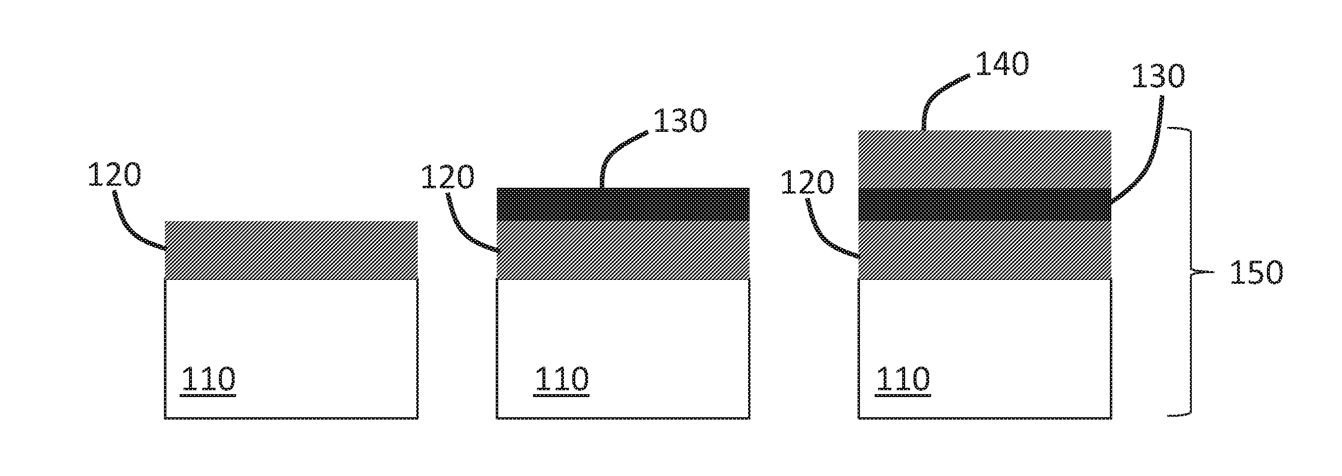
[0016] FIGS. 1A-1C illustrate a method of fabricating a semiconductor device using a two-dimensional (2D) material layer for dislocation filtering.
[0017] FIGS. 2A-2C illustrate a method of fabricating a semiconductor device using remote epitaxy on a 2D material layer.
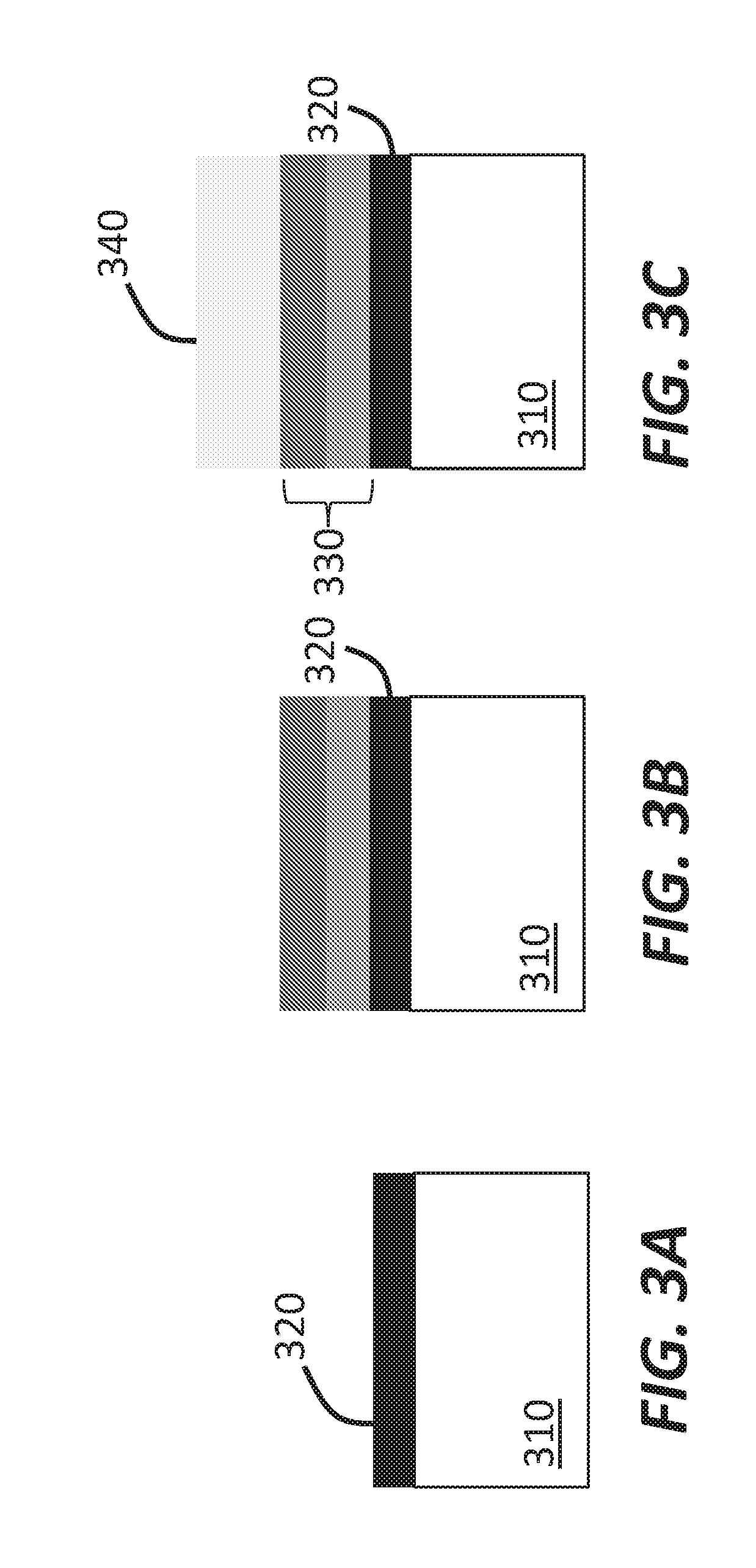
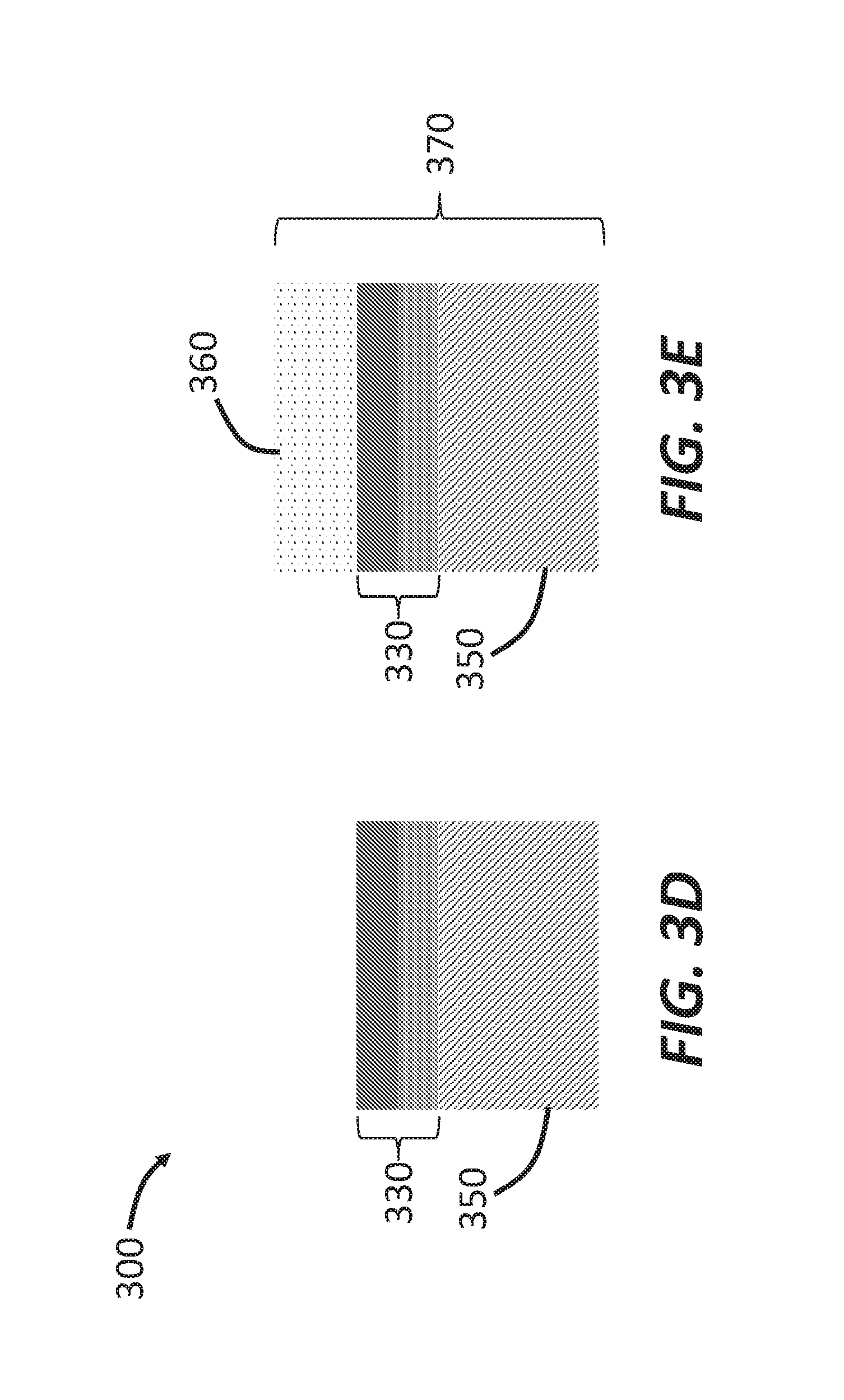
[0018] FIGS. 3A-3E illustrate a method of fabricating a semiconductor device based on a graded buffer layer.
[0019] FIGS. 4A and 4B show schematics of graded buffer layers fabricated on a single 2D material layer and multiple 2D material layers, respectively.
[0020] FIGS. 5A-5D illustrate a method of fabricating semiconductor devices on a reusable platform including a 2D material layer.
DETAILED DESCRIPTION
[0021] Overview
[0022] As described above, it can be desirable for a layer-transfer process to have substrate reusability, minimal needs for post-release treatment, a fast release rate, precise control of release interfaces, and universality for a wide range of device materials. Conventional layer-transfer processes may exhibit some of the desired properties. For example, layer release is much faster for mechanical lift-off than for chemical or optical lift-off, whereas the release location can be better controlled in chemical and optical lift-off. However, conventional layer-transfer methods suffer from rough surface formation after layer release, thereby limiting substrate reusability. In fact, the process cost to refurbish the substrate surface in conventional layer-transfer methods typically exceeds the substrate cost, so practical applications in manufacturing can be challenging. In addition, each conventional method usually works for a limited number of specific materials (e.g., chemical lift-off for III-V materials, whose lattice is close to that of GaAs, and optical lift-off for materials that can be grown on transparent substrates). Therefore, it is also challenging to make universal use of these methods.
[0023] To address the shortcomings in conventional layer-transfer methods, systems and methods described herein employ a layer transfer technique based on a two-dimensional (2D) material (e.g., graphene). The 2D material can perform several functions to facilitate the growth and transfer of functional layers. For example, the 2D material can function as a filter to reduce and/or eliminate dislocation in the functional layer (see, e.g., FIGS. 1A-1C). In this example, the functional layer is epitaxially grown on the 2D material, and the Van der Waals bonding between the functional layer (e.g., made of III-V semiconductor) and the 2D material can physically discontinue the dislocation at the interface.
[0024] The 2D material can also function as a release layer that allows fast, precise, and repeatable release at the surface. In this case, remote epitaxy can be combined with spontaneous relaxation to grow functional layers with low dislocation density on the 2D material, which is disposed on a substrate (also referred to as a parent substrate). The functional layers can then be readily transferred to another substrate (also referred to as a host substrate) for further processing (see, e.g., FIGS. 2A-2C), leaving the parent substrate and the 2D material for another cycle of fabrication.
[0025] The layer transfer technique can also fabricate and transfer growth substrates. For example, a graded buffer layer can be grown on the 2D material and then transferred to a host substrate to fabricate functional layers (see, e.g., FIGS. 3A-3E). Therefore, this technique can be used to construct a multi-purpose platform to accommodate different manufacturing demands.
[0026] Dislocation Filtering for Graphene-Based Layer Transfer
[0027] FIGS. 1A-1C illustrate a method 100 of fabricating a semiconductor device using a two-dimensional (2D) material layer for dislocation filtering. In the method 100, a first epitaxially layer 120 is formed on a first substrate 110 as shown in FIG. 1A. The first substrate 110 and the first epitaxial layer 120 can have different lattice structures (e.g., different lattice constants). For example, the first substrate may include a first semiconductor material having a first lattice structure (e.g., a first lattice constant) and the first epitaxial layer 120 may include a second semiconductor material having a second lattice structure different from the first lattice structure (e.g., a second lattice constant).
[0028] FIG. 1B shows that a filter layer 130 made of a two-dimensional material (2D) is formed on the first epitaxial layer 120. A second epitaxial layer 140 made of the same material as in the first epitaxial layer 120 is then grown on the filter layer 130 to form a structure 150 (also referred to as a device 150), as shown in FIG. 1C. As described above, the Van der Waals bonding between the second epitaxial layer 140 and the filter layer 130 can physically discontinue the dislocation at the interface, thereby producing high-quality crystalline structures in the second epitaxial layer 140.
[0029] The first substrate 110 can include any substrate suitable for epitaxial growth. For example, the first substrate 110 can include GaN and the first epitaxial layer 120 can include InGaN. In another example, the first substrate 110 includes GaAs and the first epitaxial layer 120 includes InGaAs. In yet another example, the first substrate 110 includes InP and the first epitaxial layer 120 includes InGaP. In yet another example, the first epitaxial layer 120 can include silicon carbide (SiC) and the first substrate 110 can include any platform that can be used to prepare SiC.
[0030] The materials of the first substrate 110 and the first epitaxial layer 120 usually can have lattice mismatch. Accordingly, the first epitaxial layer 120 can include dislocations. In practice, the lattice mismatch can be about 0% to about 70% (e.g., about 0%, about 10%, about 20%, about 30%, about 40%, about 50%, about 60%, and about 70%, including any values and sub ranges in between). However, the dislocations in the first epitaxial layer 120 not affect the quality of the second epitaxial layer 140 due to the filtering effect of the filter layer 130.
[0031] In general, a thicker first epitaxial layer 120 can result in better interface for subsequent processing but it may also take longer time to fabricate the first epitaxial layer 120. In some cases, the thickness of the first epitaxial layer 120 can be about 100 nm to about 10 .mu.m (e.g., about 100 nm, about 200 nm, about 300 nm, about 500 nm, about 1 .mu.m, about 2 .mu.m, about 3 .mu.m, about 4 .mu.m, about 5 .mu.m, about 6 .mu.m, about 7 .mu.m, about 8 .mu.m, about 9 .mu.m, or about 10 .mu.m, including any values and sub ranges in between).
[0032] Various types of 2D materials can be used for the filter layer 130. In one example, the filter layer 130 includes graphene (e.g., monolayer graphene or multilayer graphene). In another example, the filter layer 130 includes transition metal dichalcogenide (TMD) monolayers, which are atomically thin semiconductors of the type MX.sub.2, with M being a transition metal atom (e.g., Mo, W, etc.) and X being a chalcogen atom (e.g., S, Se, or Te). In a TMD lattice, one layer of M atoms is usually sandwiched between two layers of X atoms. In yet another example, the filter layer 130 can include a single-atom layer of metal, such as palladium and rhodium.
[0033] Out of these 2D materials, graphene can have several desirable properties. For example, graphene is a crystalline film and is a suitable substrate for growing epitaxial over-layers. Second, graphene's weak interaction with other materials can substantially relax the lattice mismatching rule for epitaxial growth, potentially permitting the growth of most semiconducting films with low defect densities. Third, epilayers grown on a graphene substrate can be easily and precisely released from the substrate owing to graphene's weak van der Waals interactions, thereby allowing rapid mechanical release of epilayers without post-release reconditioning of the released surface. Fourth, graphene's mechanical robustness can increase or maximize its reusability for multiple growth/release cycles.
[0034] The filter layer 130 made of graphene is also referred to as a graphene layer 130 and can be prepared via various methods. For example, the graphene layer 130 can be fabricated on another substrate (also referred to as a parent substrate, not shown in FIGS. 1A-1C). In this example, the graphene layer 130 can include an epitaxial graphene with a single-crystalline orientation and the parent substrate can include a (0001) 4H-SiC wafer with a silicon surface. The fabrication of the graphene layer 130 can include multistep annealing steps. A first annealing step can be performed in H.sub.2 gas for surface etching and vicinalization, and a second annealing step can be performed in Argon for graphitization at high temperature (e.g., about 1,575.degree. C.).
[0035] In another example, the graphene layer 130 can be grown on the parent substrate via a chemical vapor deposition (CVD) process. The parent substrate can include a nickel substrate or a copper substrate (e.g., to fabricate poly-crystalline graphene layers). Alternatively, the parent substrate can include an insulating substrate made of SiO.sub.2, HfO.sub.2, Al.sub.2O.sub.3, Si.sub.3N.sub.4, or practically any other high temperature, planar material compatible with CVD.
[0036] In yet another example, the parent substrate can be any substrate that can hold the graphene layer 130, and the fabrication can include a mechanical exfoliation process. In this example, the parent substrate can function as a temporary holder for the graphene layer 130.
[0037] Various methods can also be used to transfer the graphene layer 130 from the parent substrate to the second substrate. In one example, a carrier film can be attached to the graphene layer 130. The carrier film can include a thick film of Poly(methyl methacrylate) (PMMA) or a thermal release tape and the attachment can be achieved via a spin-coating process. After the combination of the carrier film and the graphene layer 130 is disposed on the first epitaxial layer 120, the carrier film can be dissolved (e.g., in acetone) for further fabrication of the second epitaxial layer 140 on the graphene layer 130.
[0038] In another example, a stamp layer including an elastomeric material, such as polydimethylsiloxane (PDMS), can be attached to the graphene layer 130 and the parent substrate can be etched away, leaving the combination of the stamp layer and the graphene layer 130. After the stamp layer and the graphene layer 130 are placed on the first epitaxial layer 120, the stamp layer can be removed by mechanical detachment, producing a clean surface of the graphene layer 130 for further processing.
[0039] In yet another example, a self-release transfer method can be used to transfer the graphene layer 130 to the first epitaxial layer 120. In this method, a self-release layer is first spun-cast over the graphene layer 130. An elastomeric stamp is then placed in conformal contact with the self-release layer. The parent substrate can be etched away to leave the combination of the stamp layer, the self-release layer, and the graphene layer 130. After this combination is placed on the first epitaxial layer 120, the stamp layer can be removed mechanically and the self-release layer can be dissolved under mild conditions in a suitable solvent. The release layer can include polystyrene (PS), poly(isobutylene) (PIB) and Teflon AF (poly[4,5-difluoro-2,2-bis(trifluoromethyl)-1,3-dioxole-co-tetrafluoroeth- ylene]).
[0040] The fabrication of the second epitaxial layer 140 can be carried out using any suitable semiconductor fabrication technique known in the art. For example, low-pressure Metal-Organic Chemical Vapor Deposition (MOCVD) can be used to grow the second epitaxial layer 140 (e.g., a GaN film) on the filter layer 130. In this example, the filter layer 130 and the first substrate 110 can be baked (e.g., under H.sub.2 for >15 min at >1,100.degree. C.) to clean the surface. Then the deposition of second epitaxial layer 140 including GaN can be performed at, for example, 200 mbar. Trimethylgallium, ammonia, and hydrogen can be used as the Ga source, nitrogen source, and carrier gas, respectively. A modified two-step growth process can be employed to obtain GaN epitaxial films on the graphene filter layer 130. The first step can be carried out at a growth temperature of 1,100.degree. C. for a few minutes where guided nucleation at the terrace edges can be promoted. The second growth step can be carried out at an elevated temperature of 1,250.degree. C. to promote the lateral growth. Vertical GaN growth rate in this case can be around 20 nm per min.
[0041] The second epitaxial layer 140 is also referred to as a functional layer or a device layer, which can be transferred to another substrate (also referred to as a host substrate, not shown in FIGS. 1A-1C) for further processing to fabricate various types of semiconductor devices. These devices include, for example, solar cells, photodetectors, transistors, light-emitting diodes (LEDs), and semiconductor layers, among others. After the second epitaxial layer 140 is transferred out, the remaining platform, including the filter layer 130, the first epitaxial layer 120, and the first substrate 110, can be used to form another epitaxial layer (e.g., a third epitaxial layer substantially similar to the second epitaxial layer 140). In some cases, the filter layer 130 can be transferred out together with the second epitaxial layer 140. A new filter layer can then be disposed on the first epitaxial layer 120 before next round of epitaxial growth. More details about transferring and further processing of the second epitaxial layer 140 can be found in PCT Application No. PCT/US2016/050701, filed Sep. 8, 2016, and entitled "SYSTEMS AND METHODS FOR GRAPHENE BASED LAYER TRANSFER," which is hereby incorporated herein by reference in its entirety.
[0042] Layer Transfer Techniques Using Remote Epitaxy
[0043] FIGS. 2A-2C illustrate a method 200 of fabricating a semiconductor device using remote epitaxy on a 2D material layer. In the method 200, a 2D material layer 220 (also referred to as a 2D layer 220) is formed directly on a first substrate 210 as shown in FIG. 2A. FIG. 2B shows that an epitaxial layer 230 is grown on the 2D layer 220. The first substrate 210 includes a first semiconductor material having a first lattice constant, and the epitaxial layer 230 includes a second semiconductor material having a second lattice constant different from the first lattice constant. FIG. 2C shows that the epitaxial layer 230 is transferred to a host substrate 240 to form a structure 250 for further processing (e.g., forming semiconductor devices such as solar cells, photodetectors, transistors, LEDs, and semiconductor layers, among others).
[0044] Although the first semiconductor material in the first substrate 210 and the second semiconductor material in the epitaxial layer 230 usually have lattice mismatch, the surface of the epitaxial layer 230 can be substantially free of dislocation if the thickness of the epitaxial layer 230 is greater than a threshold value (also referred to as a critical thickness). For example, the thickness of the epitaxial layer 230 can be about 50 nm to about 5 .mu.m (e.g., about 50 nm, about 100 nm, about 200 nm, about 300 nm, about 500 nm, about 1 .mu.m, about 2 .mu.m, about 3 .mu.m, about 4 .mu.m, or about 5 .mu.m, including any values and sub ranges in between). The lattice mismatch between the first semiconductor material and the second semiconductor material can be about 0% to about 70% (e.g., about 0%, about 10%, about 20%, about 30%, about 40%, about 50%, about 60%, and about 70%, including any values and sub ranges in between).
[0045] The first substrate 210 can include any substrate suitable for epitaxial growth, and the epitaxial layer 230 can include any material compatible with the first substrate 210. In one example, the first substrate 210 includes GaN and the epitaxial layer 230 includes InGaN. In another example, the first substrate 210 includes GaAs and the epitaxial layer 230 includes InGaP. In yet another example, the first substrate 210 includes InP and the epitaxial layer 230 includes InGaAs.
[0046] The 2D layer 220 mostly functions as a release layer in the method 200. In one example, the 2D layer 220 includes graphene, and the thickness of the 2D layer 220 can be substantially equal to or less than 1 nm (e.g., about 1 nm, about 0.9 nm, about 0.8 nm, about 0.7 nm, about 0.6 nm, about 0.5 nm, or less, including any values and sub ranges in between).
[0047] The epitaxial layer 230 can be transferred to the host substrate 240 via any of the techniques described herein or in International Application NO. PCT/US2016/050701 Application that is incorporated herein by reference in its entirety. For example, a metal stressor can be formed on the epitaxial layer 230 and a flexible tape can then be disposed on the metal stressor. The epitaxial layer 230 can then be transferred by pulling the epitaxial layer 230 and the metal stressor off the 2D layer 220 with the flexible tape.
[0048] The host substrate 240 can include any suitable substrate to hold the epitaxial layer 230 for further processing. Examples of the host substrate 230 can include semiconductor, plastic sheet, and metal foil, among others.
[0049] After the epitaxial layer 230 has been moved to the host substrate 240, the remaining platform, including the 2D layer 220 disposed on the first substrate 210, can be used for another round of epitaxial growth. For example, a second epitaxial layer, which can be substantially similar to the epitaxial layer 230, can be grown on the 2D layer 220. In some cases, the new epitaxial layer can be different from the epitaxial layer 230. For example, they can have different thicknesses or different material compositions. This process can be repeated many times (e.g., about 50 times, about 100 times, or more) until, for example, the 2D layer 220 is damaged. At this point, the damaged 2D layer 220 can be removed (e.g., via exfoliation due to the low interaction strength of 2D materials with the first substrate 210) and a new 2D layer can be disposed on the first substrate 210.
[0050] Layer Transfer Techniques Using Graded Buffer Layers
[0051] FIGS. 3A-3E illustrate a method 300 of fabricating a semiconductor device using a graded buffer layer 300. FIG. 3A shows that a 2D layer 320 is disposed on a first substrate 310. The 2D layer 320 and the first substrate 310 can be substantially similar to the 2D layer 220 and the first substrate 210 shown in FIGS. 2A-2C and described above. FIG. 3B shows that a graded buffer layer 330 is formed on the 2D layer 320. The graded buffer layer 330 includes a first sub layer 332 having a first lattice constant and a second sub layer 334 having a second lattice constant different from the first lattice constant. A handle layer 340 is then formed on the graded buffer layer 330 as illustrated in FIG. 3C. The handle layer 340 can facilitate the transfer of the graded buffer layer 330 to a host substrate 350 as illustrated in FIG. 3D. In FIG. 3E, a device layer 360 is formed (e.g., via epitaxial growth) on the graded buffer layer 330 to form a structure 370 for further processing.
[0052] The lattice parameters of the graded buffer layer 330 are preferably selected to achieve lattice matching and an epitaxial relation with the layers that they contact at their extremities. For example, the graded buffer layer 330 can be epitaxial to the first substrate 310, graded in composition through its thickness, and epitaxial to the device layer 360 on the other side. In other words, the first sub layer 332 can be epitaxial to the first substrate 310 and the second sub-layer 334 can be epitaxial to the device layer 360.
[0053] In FIGS. 3A-3E, only two sub layers (332 and 334) are illustrated. In practice, the number of sub layers in the graded buffer layer 330 can be greater than 2 (e.g., 3 sub layers, 5 sub layers, 10 sub layers, 15 sub layers, 20 sub layers, or more, including any values and sub ranges in between). The lattice constants of the sub layers can be monotonically changing through the thickness of the graded buffer layer 330. The ith sub layer in the graded buffer layer 330 can have a corresponding lattice constant a.sub.i. In one example, the lattice constant can monotonically increase along the thickness, i.e., a.sub.i<a.sub.i+1. Alternatively, the lattice constant can monotonically decrease along the thickness, i.e., a.sub.i>a.sub.i+1.
[0054] The total thickness of the graded buffer layer 330 can depend on the number of sub layers. For example, the total thickness of the graded buffer layer 330 be about 1 .mu.m to about 10 .mu.m (e.g., about 1 .mu.m, about 2 .mu.m, about 3 .mu.m, about 4 .mu.m, about 5 .mu.m, about 6 .mu.m, about 7 .mu.m, about 8 .mu.m, about 9 .mu.m, or about 10 .mu.m, including any values and sub ranges in between). The thickness of each sub layer can be, for example, about 50 nm to about 2 .mu.m (e.g., about 50 nm, about 100 nm, about 200 nm, about 300 nm, about 500 nm, about 1 .mu.m, or about 2 .mu.m, including any values and sub ranges in between).
[0055] Using the graded buffer layer 330 can achieve the desired lattice matching and epitaxial relationship through the thickness of the resulting structure shown in FIG. 3E. This lattice matching and epitaxial relationship can reduce internal stresses and strains and promote good electron movement through the thickness of the structure shown in FIG. 3E. The graded buffer layer 330 can also relax the lattice matching of the device layer 360, so that the compositions of the device layer 360 may be configured to produce the desired bandgap for practical functions (e.g., photo conversion in solar cells, or photo detection in photodetectors), instead of producing exact lattice matching.
[0056] The distribution of the lattice constant within the graded buffer layer 330 can be controlled by the composition of each sub layer in the graded buffer layer 330. For example, the graded buffer layer 330 can include InGaAs and the lattice constant of the graded buffer layer 330 can be adjusted by changing the In to Ga ratio in each sub layer. In this case, the first substrate 310 can include GaAs and the device layer 360 can include InGaAs. The first sub layer (in contact with the 2D layer 320) in the graded buffer layer 330 can be GaAs (i.e., no In), and the amount of Ga gradually decreases and the amount of In gradually increases until the last sub layer (in contact with the device layer 360) is epitaxial to InGaAs. Similarly, the In to Ga ratio can also be used to change the lattice constant of InGaP.
[0057] The handle layer 340 can further include a stressor that is disposed on the graded buffer layer 330 and a tape layer disposed on the stressor for handling the stressor. For example, the stressor can include a high-stress metal film such as a Ni film. In this example, the Ni stressor can be deposited in an evaporator at a vacuum level of 1.times.10.sup.-5 Torr. Using the tape and the stressor together can mechanically exfoliate the graded buffer layer 330 from the 2D layer 320 at a fast release rate by applying high strain energy to the interface between the graded buffer layer 330 and the 2D layer 320. The release rate can be fast at least due to the weak van der Waals bonding between the 2D material in the 2D layer 320 (e.g., graphene) and the material such as the graded buffer layer 330 (e.g., GaAs).
[0058] FIG. 3D also shows that the handle layer 340 is removed, leaving the graded buffer layer 330 for the growth of the device layer 360. In one example, the handle layer (e.g., including the tape layer and the stressor) can be etched away by a FeCl.sub.3-based solution.
[0059] FIGS. 4A and 4B show schematics of graded buffer layers fabricated on a single 2D material layer and multiple 2D material layers, respectively. FIG. 4A shows a semiconductor device 401 including a graded buffer layer 431 fabricated on a graphene layer 421, which in turn is disposed on a substrate 411. The graded buffer layer 431 includes multiple sub layers 431(1) to 431(n), where n is a positive integer. The number of sub layers n can be, for example, greater than 2 (e.g., 3 sub layers, 5 sub layers, 10 sub layers, 15 sub layers, 20 sub layers, or more, including any values and sub ranges in between). In the system 401, the sub layers 431(1) to 431(n) are directly stacked together without any spacers. During fabrication, the sub layer 432(i+1) is deposited on the sub layer 432(i), i=1, 2, . . . , n-1.
[0060] FIG. 4B shows a semiconductor device 402 including a graded buffer layer 432 disposed on a substrate 412. The graded buffer layer 432 includes multiple sub layers 432(1), 432(2), . . . , 432(n), and adjacent sub layers 432(i) and 432(i+1) are separated by a corresponding graphene layer 422(i+1). In the system 402, the first graphene layer 422(1) is disposed on the substrate 412 on which the first sub layer 432(1) is formed. A second graphene layer 422(2) is then disposed on the first sub layer 432(1), and the process continues until the last sub layer 432(n) is formed. In general, using a graded buffer layer (431 or 432) including multiple sub layers can filter the dislocation multiple times, thereby leading to reduced dislocation in epitaxial layers fabricated on the graded buffer.
[0061] FIGS. 5A-5D illustrate a method 500 of fabricating semiconductor devices on a reusable platform including a 2D material layer. In FIG. 5A, a graded buffer layer 530 is removed from a graphene layer 520 using a transfer handle layer 540. The graphene layer 520 is disposed on a substrate 510 to form a reusable platform 550. The graded buffer layer 530 is disposed on a host substrate 560 as shown in FIG. 5B. The handle layer 540 is then removed (e.g., via etching) to expose the surface of the graded buffer layer 530 for further processing (e.g., epitaxial growth of device layers). The reusable platform 550, including the graphene layer 520 disposed on the substrate 510, can be used to form a new graded buffer layer, as shown in FIG. 5D. In one example, the new graded buffer layer can be substantially similar to the graded buffer layer 530. In another example, the new graded buffer layer can be different from the graded buffer layer 530. For example, these two graded buffer layers can have different material compositions or different numbers of sub layers.
[0062] In some cases, the reusable platform 550 can be used to fabricate device layers (e.g., epitaxial layer 230 in FIGS. 2A-2C). Accordingly, the reusable platform 550 can be configured as a multi-function platform to accommodate different fabrication demands (e.g., fabricate device layers at one time and fabricate graded buffer layers at another time, without changing hardware components in the platform 550).
CONCLUSION
[0063] While various inventive embodiments have been described and illustrated herein, those of ordinary skill in the art will readily envision a variety of other means and/or structures for performing the function and/or obtaining the results and/or one or more of the advantages described herein, and each of such variations and/or modifications is deemed to be within the scope of the inventive embodiments described herein. More generally, those skilled in the art will readily appreciate that all parameters, dimensions, materials, and configurations described herein are meant to be exemplary and that the actual parameters, dimensions, materials, and/or configurations will depend upon the specific application or applications for which the inventive teachings is/are used. Those skilled in the art will recognize, or be able to ascertain using no more than routine experimentation, many equivalents to the specific inventive embodiments described herein. It is, therefore, to be understood that the foregoing embodiments are presented by way of example only and that, within the scope of the appended claims and equivalents thereto, inventive embodiments may be practiced otherwise than as specifically described and claimed. Inventive embodiments of the present disclosure are directed to each individual feature, system, article, material, kit, and/or method described herein. In addition, any combination of two or more such features, systems, articles, materials, kits, and/or methods, if such features, systems, articles, materials, kits, and/or methods are not mutually inconsistent, is included within the inventive scope of the present disclosure.
[0064] Also, various inventive concepts may be embodied as one or more methods, of which an example has been provided. The acts performed as part of the method may be ordered in any suitable way. Accordingly, embodiments may be constructed in which acts are performed in an order different than illustrated, which may include performing some acts simultaneously, even though shown as sequential acts in illustrative embodiments.
[0065] All definitions, as defined and used herein, should be understood to control over dictionary definitions, definitions in documents incorporated by reference, and/or ordinary meanings of the defined terms.
[0066] The indefinite articles "a" and "an," as used herein in the specification and in the claims, unless clearly indicated to the contrary, should be understood to mean "at least one."
[0067] The phrase "and/or," as used herein in the specification and in the claims, should be understood to mean "either or both" of the elements so conjoined, i.e., elements that are conjunctively present in some cases and disjunctively present in other cases. Multiple elements listed with "and/or" should be construed in the same fashion, i.e., "one or more" of the elements so conjoined. Other elements may optionally be present other than the elements specifically identified by the "and/or" clause, whether related or unrelated to those elements specifically identified. Thus, as a non-limiting example, a reference to "A and/or B", when used in conjunction with open-ended language such as "comprising" can refer, in one embodiment, to A only (optionally including elements other than B); in another embodiment, to B only (optionally including elements other than A); in yet another embodiment, to both A and B (optionally including other elements); etc.
[0068] As used herein in the specification and in the claims, "or" should be understood to have the same meaning as "and/or" as defined above. For example, when separating items in a list, "or" or "and/or" shall be interpreted as being inclusive, i.e., the inclusion of at least one, but also including more than one, of a number or list of elements, and, optionally, additional unlisted items. Only terms clearly indicated to the contrary, such as "only one of" or "exactly one of," or, when used in the claims, "consisting of," will refer to the inclusion of exactly one element of a number or list of elements. In general, the term "or" as used herein shall only be interpreted as indicating exclusive alternatives (i.e., "one or the other but not both") when preceded by terms of exclusivity, such as "either," "one of," "only one of," or "exactly one of" "Consisting essentially of," when used in the claims, shall have its ordinary meaning as used in the field of patent law.
[0069] As used herein in the specification and in the claims, the phrase "at least one," in reference to a list of one or more elements, should be understood to mean at least one element selected from any one or more of the elements in the list of elements, but not necessarily including at least one of each and every element specifically listed within the list of elements and not excluding any combinations of elements in the list of elements. This definition also allows that elements may optionally be present other than the elements specifically identified within the list of elements to which the phrase "at least one" refers, whether related or unrelated to those elements specifically identified. Thus, as a non-limiting example, "at least one of A and B" (or, equivalently, "at least one of A or B," or, equivalently "at least one of A and/or B") can refer, in one embodiment, to at least one, optionally including more than one, A, with no B present (and optionally including elements other than B); in another embodiment, to at least one, optionally including more than one, B, with no A present (and optionally including elements other than A); in yet another embodiment, to at least one, optionally including more than one, A, and at least one, optionally including more than one, B (and optionally including other elements); etc.
[0070] In the claims, as well as in the specification above, all transitional phrases such as "comprising," "including," "carrying," "having," "containing," "involving," "holding," "composed of," and the like are to be understood to be open-ended, i.e., to mean including but not limited to. Only the transitional phrases "consisting of" and "consisting essentially of" shall be closed or semi-closed transitional phrases, respectively, as set forth in the United States Patent Office Manual of Patent Examining Procedures, Section 2111.03.
* * * * *
D00000
D00001
D00002
D00003
D00004
D00005
D00006
XML
uspto.report is an independent third-party trademark research tool that is not affiliated, endorsed, or sponsored by the United States Patent and Trademark Office (USPTO) or any other governmental organization. The information provided by uspto.report is based on publicly available data at the time of writing and is intended for informational purposes only.
While we strive to provide accurate and up-to-date information, we do not guarantee the accuracy, completeness, reliability, or suitability of the information displayed on this site. The use of this site is at your own risk. Any reliance you place on such information is therefore strictly at your own risk.
All official trademark data, including owner information, should be verified by visiting the official USPTO website at www.uspto.gov. This site is not intended to replace professional legal advice and should not be used as a substitute for consulting with a legal professional who is knowledgeable about trademark law.