Zinc Nitride Compound And Method For Producing Same
OBA; Fumiyasu ; et al.
U.S. patent application number 16/387155 was filed with the patent office on 2019-08-15 for zinc nitride compound and method for producing same. The applicant listed for this patent is Panasonic Corporation. Invention is credited to Lee Alan BURTON, Yoyo HINUMA, Hidenori HIRAMATSU, Hideo HOSONO, Soshi IIMURA, Yu KUMAGAI, Hideya KUMOMI, Yoshinori MURABA, Fumiyasu OBA, Isao TANAKA.
| Application Number | 20190248670 16/387155 |
| Document ID | / |
| Family ID | 58517196 |
| Filed Date | 2019-08-15 |


| United States Patent Application | 20190248670 |
| Kind Code | A1 |
| OBA; Fumiyasu ; et al. | August 15, 2019 |
ZINC NITRIDE COMPOUND AND METHOD FOR PRODUCING SAME
Abstract
The present invention provides a zinc nitride compound suitable for electronic devices such as high-speed transistors, high-efficiency visible light-emitting devices, high-efficiency solar cells, and high-sensitivity visible light sensors. The zinc nitride compound is represented, for example, by the chemical formula CaZn.sub.2N.sub.2 or the chemical formula X.sup.1.sub.2ZnN.sub.2 wherein X.sup.1 is Be or Mg. The zinc nitride compound is preferably synthesized at a high pressure of 1 GPa or more.
| Inventors: | OBA; Fumiyasu; (Tokyo, JP) ; HOSONO; Hideo; (Tokyo, JP) ; HIRAMATSU; Hidenori; (Tokyo, JP) ; KUMOMI; Hideya; (Tokyo, JP) ; KUMAGAI; Yu; (Tokyo, JP) ; IIMURA; Soshi; (Tokyo, JP) ; MURABA; Yoshinori; (Tokyo, JP) ; BURTON; Lee Alan; (Tokyo, JP) ; TANAKA; Isao; (Kyoto, JP) ; HINUMA; Yoyo; (Chiba, JP) | ||||||||||
| Applicant: |
|
||||||||||
|---|---|---|---|---|---|---|---|---|---|---|---|
| Family ID: | 58517196 | ||||||||||
| Appl. No.: | 16/387155 | ||||||||||
| Filed: | April 17, 2019 |
Related U.S. Patent Documents
| Application Number | Filing Date | Patent Number | ||
|---|---|---|---|---|
| 15767550 | Aug 30, 2018 | 10308521 | ||
| PCT/JP2016/080597 | Oct 14, 2016 | |||
| 16387155 | ||||
| Current U.S. Class: | 1/1 |
| Current CPC Class: | C01P 2002/72 20130101; C01P 2002/77 20130101; Y02P 70/521 20151101; C09K 11/55 20130101; C09K 11/0883 20130101; C01G 9/006 20130101; Y02P 70/50 20151101; C01P 2006/40 20130101; H01L 31/0256 20130101; H01L 29/24 20130101; C01B 21/0602 20130101; C01G 9/08 20130101; H01L 31/0248 20130101; H01L 31/032 20130101; H01L 33/26 20130101; C09K 11/54 20130101; H01L 31/18 20130101; H01L 33/00 20130101; C01G 9/00 20130101 |
| International Class: | C01G 9/08 20060101 C01G009/08; C01B 21/06 20060101 C01B021/06; H01L 33/26 20060101 H01L033/26; H01L 31/032 20060101 H01L031/032; C09K 11/08 20060101 C09K011/08; C01G 9/00 20060101 C01G009/00; H01L 31/18 20060101 H01L031/18; C09K 11/55 20060101 C09K011/55; H01L 29/24 20060101 H01L029/24 |
Foreign Application Data
| Date | Code | Application Number |
|---|---|---|
| Oct 15, 2015 | JP | 2015-203891 |
Claims
1-14. (canceled)
15. A zinc nitride compound represented by the chemical formula X.sup.1.sub.2ZnN.sub.2 wherein X.sup.1 is Be or Mg.
16. A zinc nitride compound represented by the chemical formula ZnTiN.sub.2.
17. A zinc nitride compound represented by the chemical formula Zn.sub.2X.sup.3N.sub.3 wherein X.sup.3 is V, Nb, or Ta.
18. A zinc nitride compound represented by the chemical formula Zn.sub.3WN.sub.4.
19. The zinc nitride compound according to claim 15, being a compound semiconductor.
20. The zinc nitride compound according to claim 16, being a compound semiconductor.
21. The zinc nitride compound according to claim 17, being a compound semiconductor.
22. The zinc nitride compound according to claim 18, being a compound semiconductor.
23. An electronic device comprising an active layer comprising the compound semiconductor according to claim 19.
24. An electronic device comprising an active layer comprising the compound semiconductor according to claim 20.
25. An electronic device comprising an active layer comprising the compound semiconductor according to claim 21.
26. An electronic device comprising an active layer comprising the compound semiconductor according to claim 22.
27. The electronic device according to claim 23, wherein the electronic device emits light in the visible range under current injection.
28. The electronic device according to claim 24, wherein the electronic device emits light in the visible range under current injection.
29. The electronic device according to claim 25, wherein the electronic device emits light in the visible range under current injection.
30. The electronic device according to claim 26, wherein the electronic device emits light in the visible range under current injection.
31. The electronic device according to claim 23, wherein the electronic device generates a photovoltage or a photocurrent by absorbing visible light.
32. The electronic device according to claim 24, wherein the electronic device generates a photovoltage or a photocurrent by absorbing visible light.
33. The electronic device according to claim 25, wherein the electronic device generates a photovoltage or a photocurrent by absorbing visible light.
34. The electronic device according to claim 26 wherein the electronic device generates a photovoltage or a photocurrent by absorbing visible light.
Description
TECHNICAL FIELD
[0001] The present invention relates to a zinc nitride compound and a method for producing the same.
BACKGROUND ART
[0002] GaN is widely used in LED light sources. However, GaN has a wide band gap and therefore cannot emit light in the visible range by itself. InN has too narrow a band gap, due to which it cannot emit light in the visible range. Ga is a high-cost element, and In is a scarce element. Various zinc nitride compounds have been proposed; however, for example, ZnSnN.sub.2 is difficult to produce in the form of a p-type semiconductor, and Ca.sub.2ZnN.sub.2 is an indirect band gap semiconductor. The problem with these zinc nitride compounds is that, for example, they are unsuitable for use in light-emitting devices or high-efficiency solar cells (Non Patent Literature 1).
CITATION LIST
Non Patent Literature
[0003] Non Patent Literature 1; J. Solid State Chem. 88, 528-533 (1990)
SUMMARY OF INVENTION
Technical Problem
[0004] It is an object of the present invention to solve the above problem and provide a zinc nitride compound suitable for electronic devices such as high-speed transistors, high-efficiency visible light-emitting devices, high-efficiency solar cells, and high-sensitivity visible light sensors.
Solution to Problem
[0005] The present disclosure provides the following inventions to solve the above problem.
[0006] (1) A zinc nitride compound represented by the chemical formula CaZn.sub.2N.sub.2.
[0007] (2) A zinc nitride compound represented by the chemical formula X.sup.1.sub.2ZnN.sub.2 wherein X.sup.1 is Be or Mg.
[0008] (3) A zinc nitride compound represented by the chemical formula Zn.sub.3LaN.sub.3.
[0009] (4) A zinc nitride compound represented by the chemical formula ZnTiN.sub.2.
[0010] (5) A zinc nitride compound represented by the chemical formula ZnX.sup.2N.sub.2 wherein X.sup.2 is Zr or Hf.
[0011] (6) A zinc nitride compound represented by the chemical formula Zn.sub.2X.sup.3N.sub.3 wherein X.sup.3 is V, Nb, or Ta.
[0012] (7) A zinc nitride compound represented by the chemical formula Zn.sub.3WN.sub.4.
[0013] (8) The zinc nitride compound according to any one of (1) to (7), being a compound semiconductor.
[0014] (9) The zinc nitride compound according to (1) or (3), being a direct band gap compound semiconductor.
[0015] (10) A compound semiconductor represented by the chemical formula CaM.sup.1.sub.2xZn.sub.2(1-x)N.sub.2 wherein M.sup.1 is Mg or Cd and 0.ltoreq.x.ltoreq.1 or M.sup.2.sub.xxCa.sub.1-xZn.sub.2N.sub.2 wherein M.sup.2 is Sr or Ba and 0.ltoreq.x.ltoreq.1, the compound semiconductor having a band gap of 0.4 eV to 3.2 eV.
[0016] (11) An electronic device including an active layer including the compound semiconductor according to any one of (8) to (10).
[0017] (12) The electronic device according to (11), wherein the electronic device emits light in the visible range under current injection.
[0018] (13) The electronic device according to (11), wherein the electronic device generates a photovoltage or a photocurrent by absorbing visible light.
[0019] (14) A method for producing the zinc nitride compound according to any one of (1) to (7), including synthesizing the zinc nitride compound at a high pressure of 1 GPa or more.
Advantageous Effects of Invention
[0020] The zinc nitride compound of the present invention can be provided as a zinc nitride compound suitable for electronic devices such as high-speed transistors, high-efficiency visible light-emitting devices, high-efficiency solar cells, and high-sensitivity visible light sensors.
BRIEF DESCRIPTION OF DRAWINGS
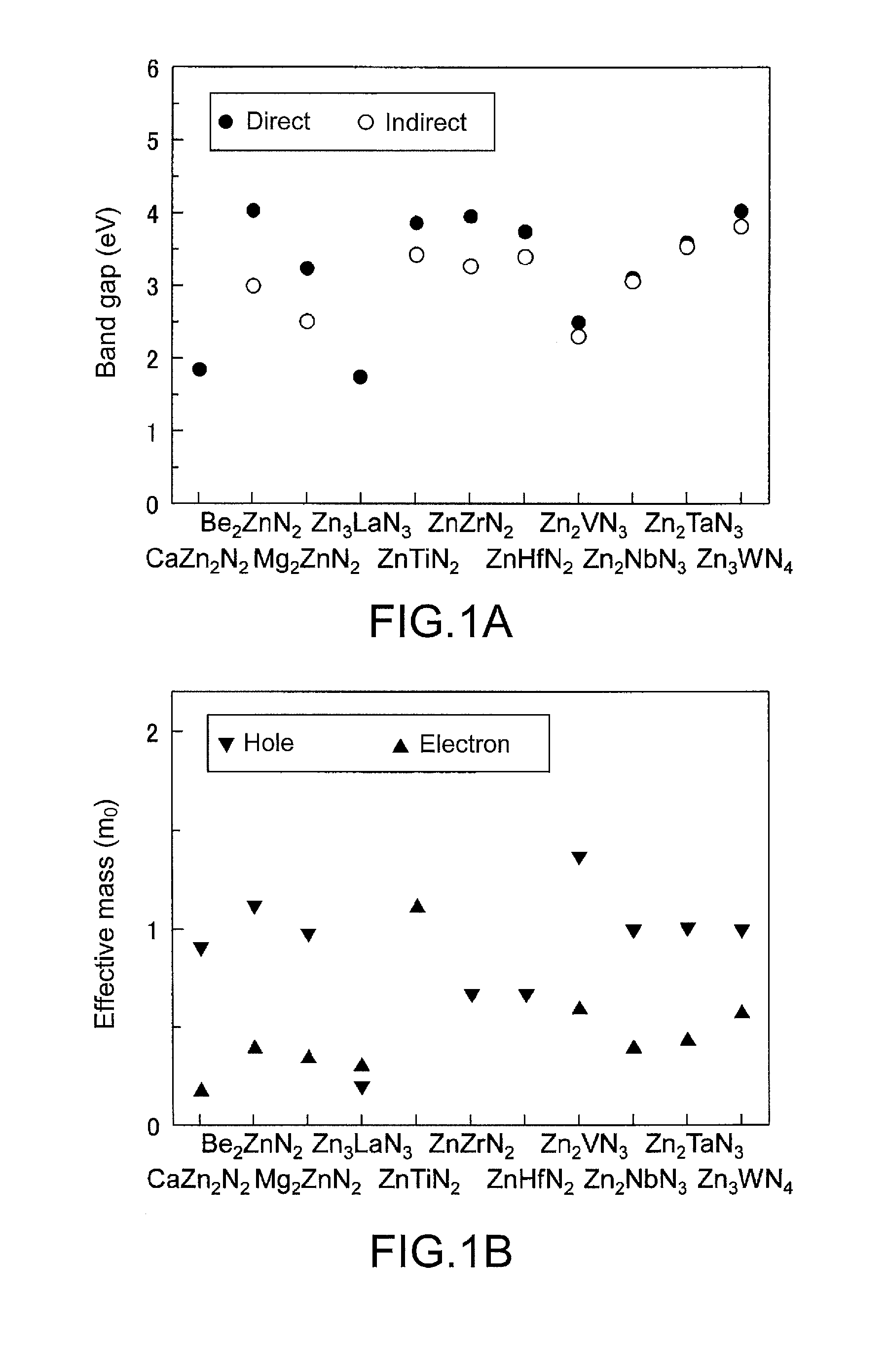
[0021] FIG. 1 shows the basic electronic properties of zinc nitride compounds according to the present invention.
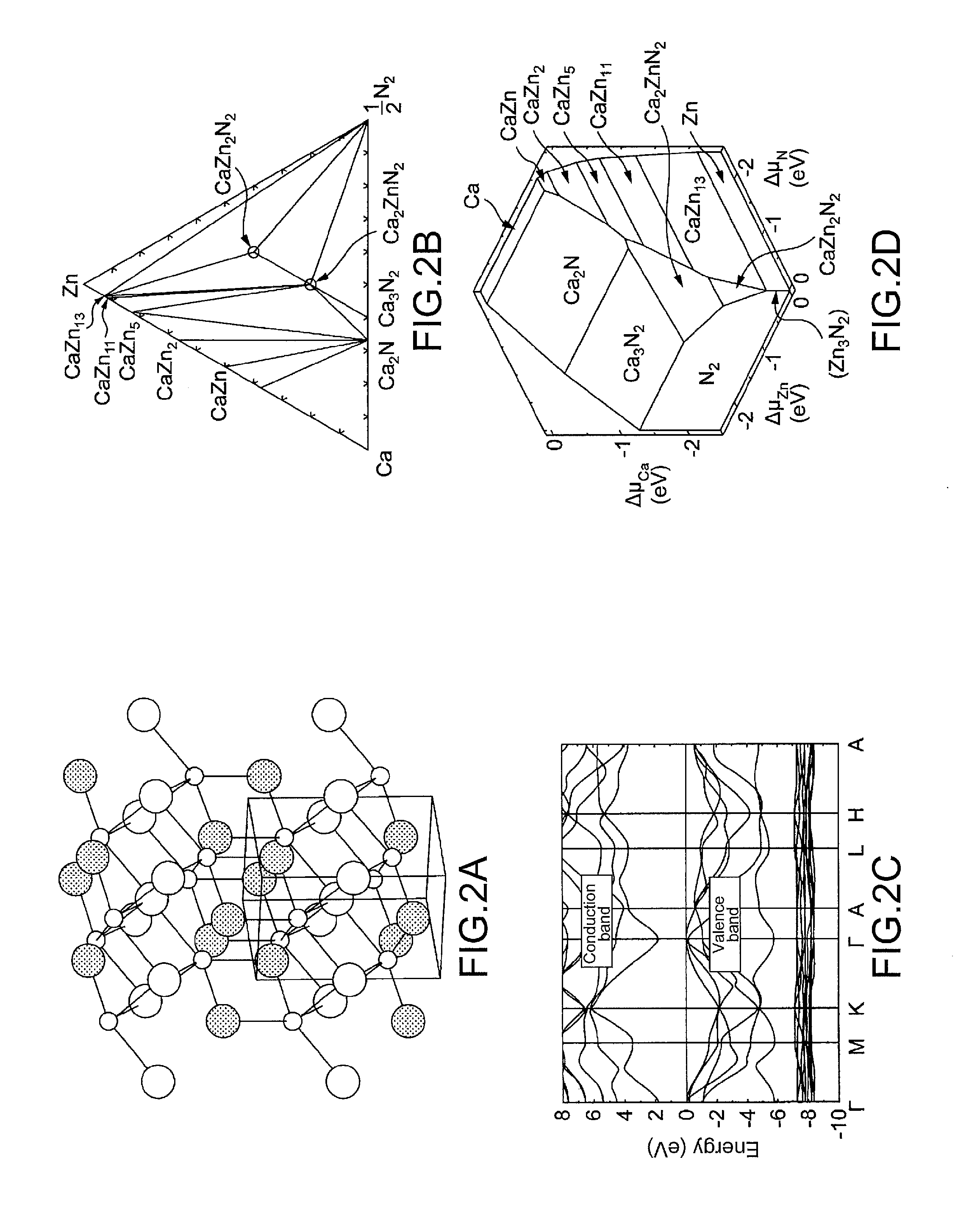
[0022] FIG. 2a shows the crystal structure of the zinc nitride compound represented by the chemical formula CaZn.sub.2N.sub.2, FIG. 2b shows the calculated phase diagram of the Ca--Zn--N system, FIG. 2c shows the band structure (conduction band and valence band) of the zinc nitride compound represented by CaZn.sub.2N.sub.2, and FIG. 2d shows the phase diagram of the Ca--Zn--N system in the chemical potential space.
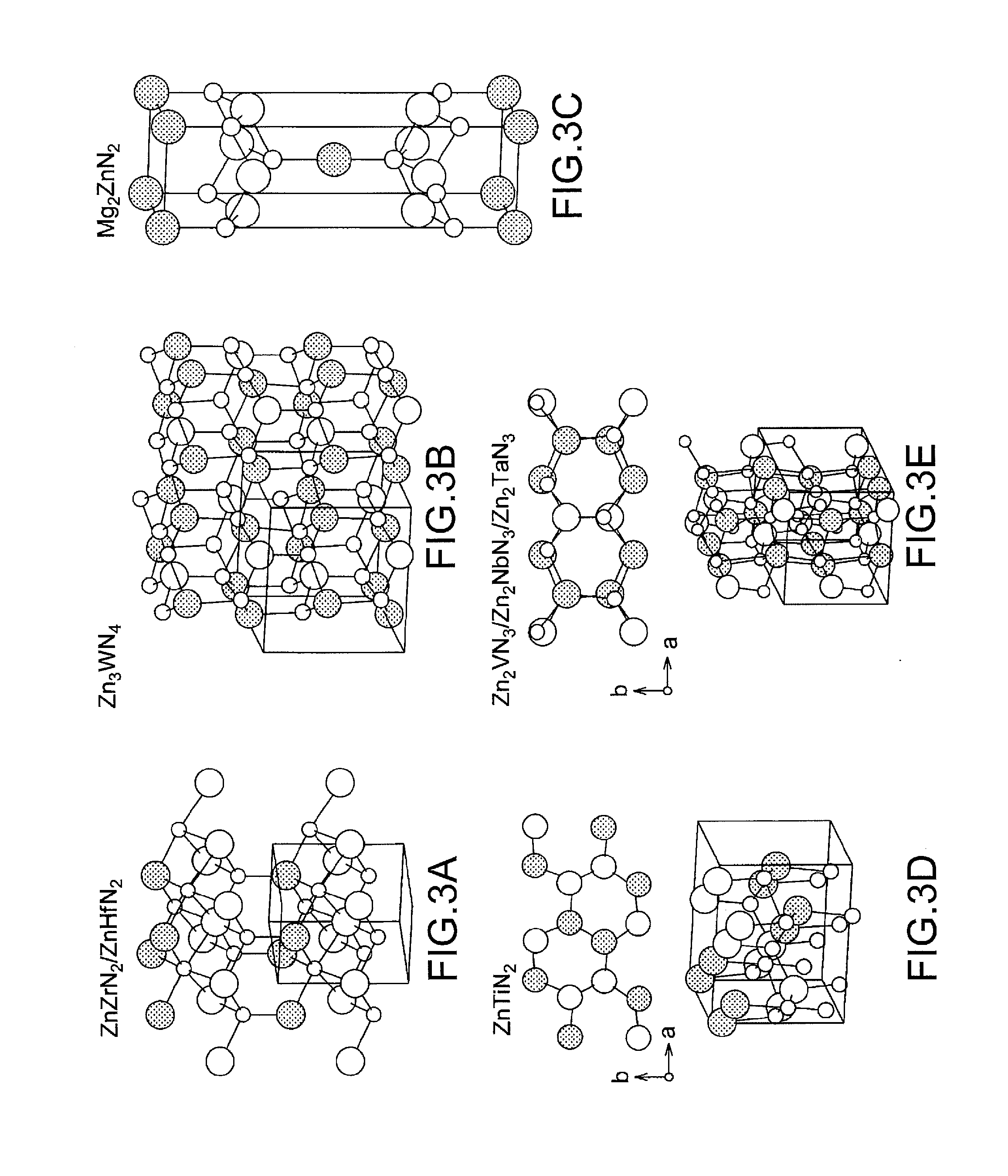
[0023] FIG. 3 shows the crystal structures of typical zinc nitride compounds of the present invention other than the zinc nitride compound A) represented by the chemical formula CaZn.sub.2N.sub.2.
[0024] FIG. 4 shows the calculated phase diagrams of the systems such as the Mg--Zn--N system for the typical zinc nitride compounds of the present invention other than the zinc nitride compound A) represented by the chemical formula CaZn.sub.2N.sub.2.
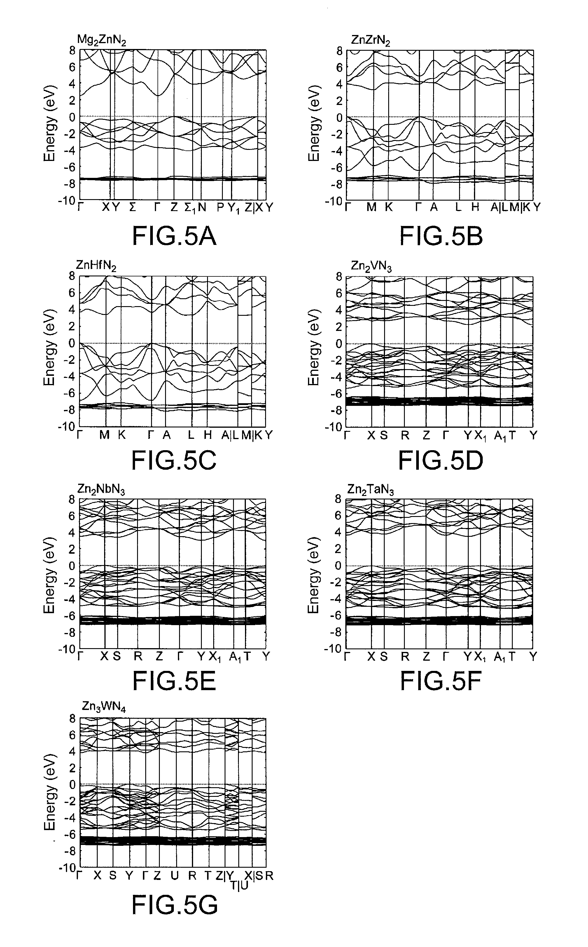
[0025] FIG. 5 shows the band structures (conduction bands and valence bands) of the typical zinc nitride compounds of the present invention other than the zinc nitride compound A) represented by the chemical formula CaZn.sub.2N.sub.2.
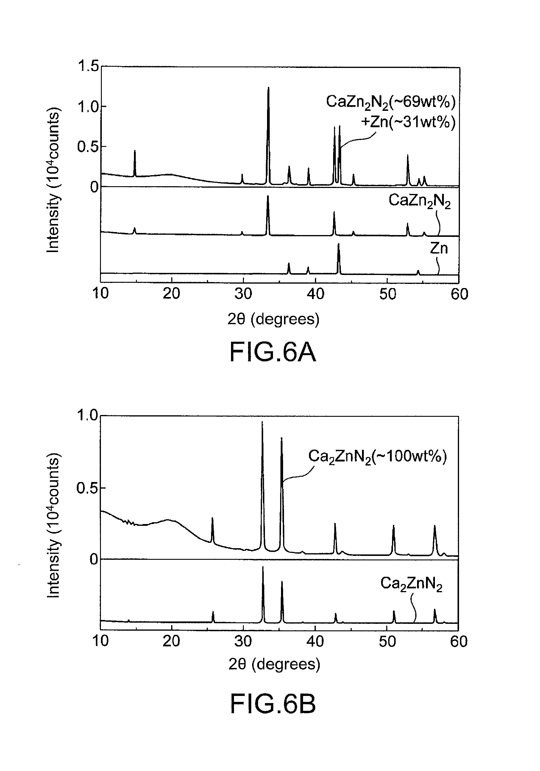
[0026] FIG. 6 shows X-ray diffraction patterns of synthesis products obtained in Example 1 and Comparative Example 1.
[0027] FIG. 7 shows absorption spectra of the synthesis products obtained in Example 1 and Comparative Example 1.
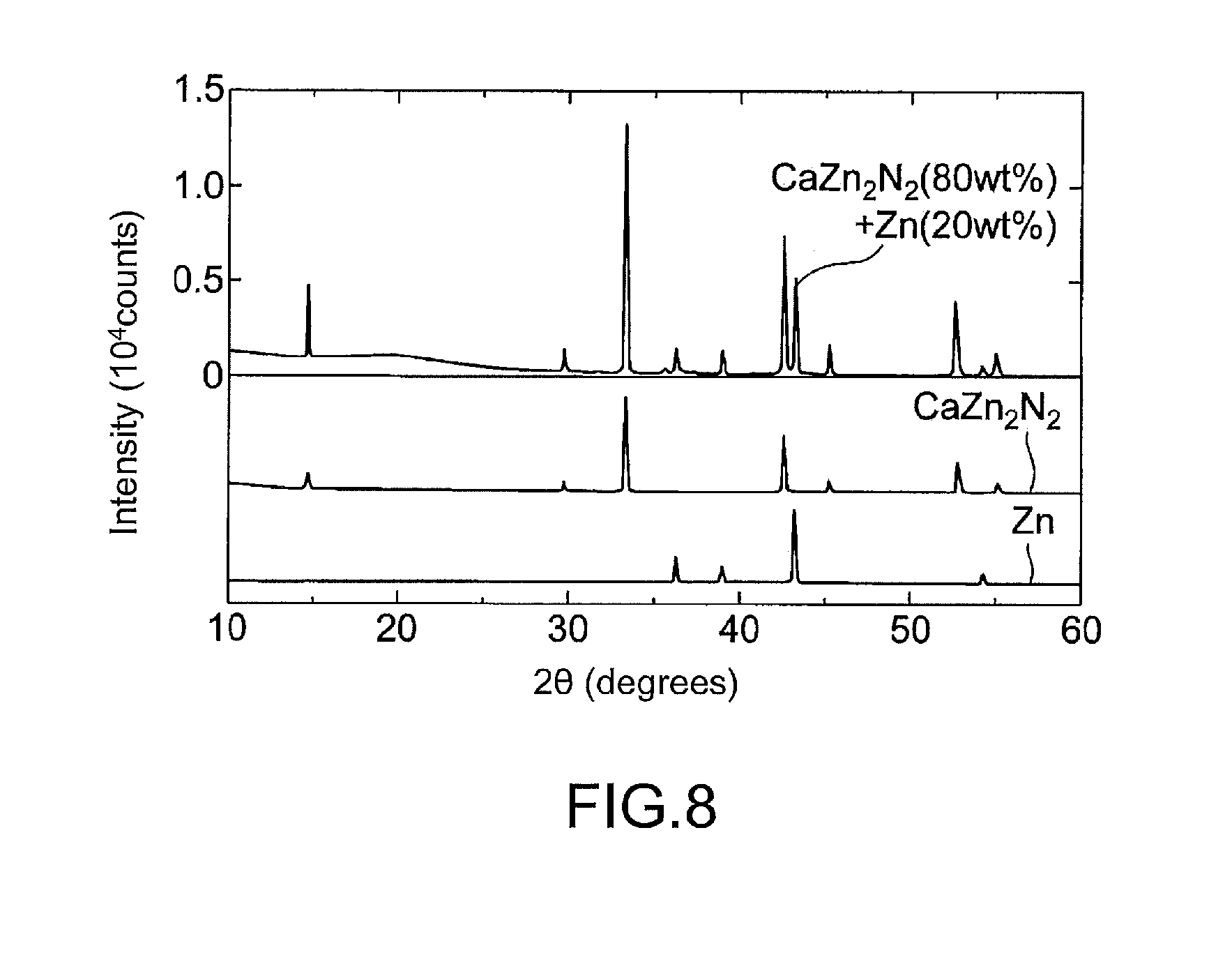
[0028] FIG. 8 shows X-ray diffraction patterns of a synthesis product obtained in Example 2.
[0029] FIG. 9 shows photoluminescence spectra of the synthesis product obtained in Example 2.
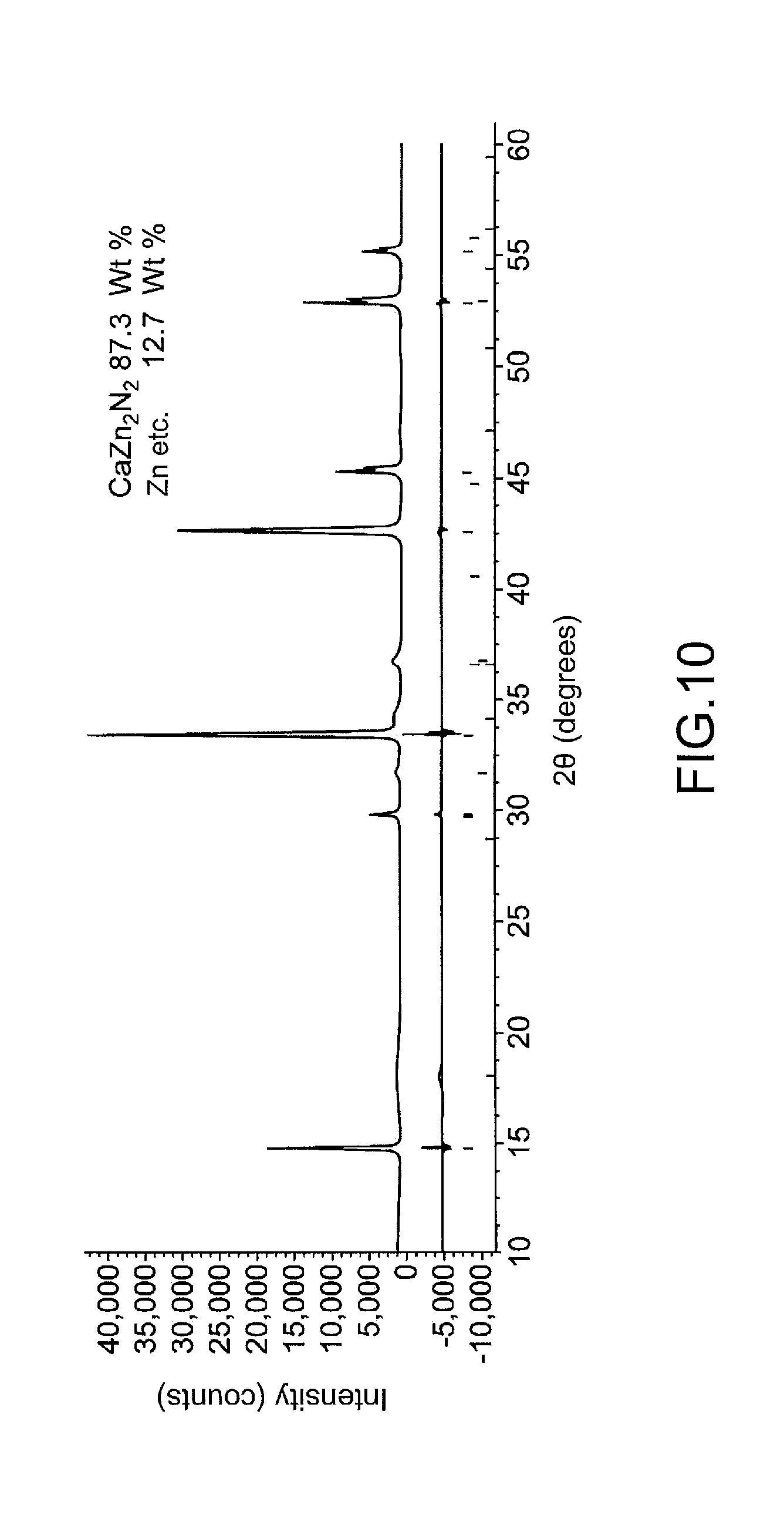
[0030] FIG. 10 shows X-ray diffraction patterns of a purified powder product obtained in Example 2.
DESCRIPTION OF EMBODIMENTS
[0031] The zinc nitride compound of the present invention can be represented by any one of the following chemical formulae.
[0032] A) A zinc nitride compound represented by the chemical formula CaZn.sub.2N.sub.2.
[0033] B) A zinc nitride compound represented by the chemical formula X.sup.1.sub.2ZnN.sub.2 wherein X.sup.1 is Be or Mg.
[0034] C) A zinc nitride compound represented by the chemical formula Zn.sub.3LaN.sub.3.
[0035] D) A zinc nitride compound represented by the chemical formula ZnTiN.sub.2.
[0036] E) A zinc nitride compound represented by the chemical formula ZnX.sup.2N.sub.2 wherein X.sup.2 is Zr or Hf.
[0037] F) A zinc nitride compound represented by the chemical formula Zn.sub.2X.sup.3N.sub.3 wherein X.sup.3 is V, Nb, or Ta.
[0038] G) A zinc nitride compound represented by the chemical formula Zn.sub.3WN.sub.4.
[0039] The zinc nitride compounds A) to G) according to the present invention are novel compounds which are not included in Inorganic Crystal Structure Database (ICSD). The basic electronic properties of the zinc nitride compounds A) to G) according to the present invention are shown in FIG. 1. In FIG. 1, a shows the band gaps (.circle-solid. represents a direct band gap, while o represents an indirect band gap), and b shows the effective masses of holes and electrons. The zinc nitride compounds according to the present invention are compound semiconductors. In particular, the zinc nitride compound A) or C) according to the present invention which is represented by the chemical formula CaZn.sub.2N.sub.2 or Zn.sub.3LaN.sub.3 is a direct band gap compound semiconductor and suitable for use, for example, in light-emitting devices and thin-film solar cells.
[0040] The space groups to which the zinc nitride compounds according to the present invention belong are as follows.
[0041] The zinc nitride compound A) belongs to the space group P-3m1.
[0042] The zinc nitride compound B) belongs to the space group I4/mmm.
[0043] The zinc nitride compound C) belongs to the space group P6.sub.3/m.
[0044] The zinc nitride compound D) belongs to the space group Pna2.sub.1.
[0045] The zinc nitride compound E) belongs to the space group P3m1.
[0046] The zinc nitride compound F) belongs to the space group Cmc2.sub.1.
[0047] The zinc nitride compound G) belongs to the space group Pmn2.sub.1.
[0048] Hereinafter, the zinc nitride compound A) represented by the chemical formula CaZn.sub.2N.sub.2, which is suitable as a direct band gap compound semiconductor, will be described as a representative of the zinc nitride compounds of the present invention. Understanding of the other zinc nitride compounds denoted by B) to G) can also be gained from the entire contents of the detailed description.
[0049] In FIG. 2, a shows the crystal structure of the zinc nitride compound A) represented by the chemical formula CaZn.sub.2N.sub.2, b shows the calculated phase diagram of the Ca--Zn--N system, c shows the band structure (conduction band and valence band) of the zinc nitride compound represented by CaZn.sub.2N.sub.2, and d shows the phase diagram of the Ca--Zn--N system in the chemical potential space. As seen from d, CaZn.sub.2N.sub.2 is stable at a high nitrogen chemical potential, namely at a high nitrogen partial pressure.
[0050] The zinc nitride compound A) represented by the chemical formula CaZn.sub.2N.sub.2 has a band gap of 1.9 eV. The band gap can be controlled by incorporation of Mg, Sr, Ba, or Cd, which results in a compound semiconductor represented by the chemical formula CaM.sup.1.sub.2xZn.sub.2(1-x)N.sub.2 wherein M.sup.1 is Mg or Cd and 0.ltoreq.x.ltoreq.1 or M.sup.2.sub.xCa.sub.1-xZn.sub.2N.sub.2 wherein M.sup.2 is Sr or Ba and 0.ltoreq.x.ltoreq.1 and having a band gap of 0.4 eV to 3.2 eV. CaZn.sub.2N.sub.2 can be an n-type semiconductor even when undoped, since nitrogen holes serving as shallow donors are likely to be generated in CaZn.sub.2N.sub.2. However, it is preferable to form an n-type semiconductor by doping into CaZn.sub.2N.sub.2. Furthermore, for example, a higher nitrogen partial pressure reduces carrier compensation by nitrogen holes, thus allowing the formation of a p-type semiconductor by doping into CaZn.sub.2N.sub.2.
[0051] The zinc nitride compound A) represented by the chemical formula CaZn.sub.2N.sub.2 is preferably synthesized at a high pressure of 1 GPa or more. In this case, the starting compounds, preferably Ca.sub.3N.sub.2 and 2Zn.sub.3N.sub.2, are introduced into a high-pressure synthesis apparatus and reacted typically at 800 to 1500.degree. C. and 1 to 10 GPa for about 30 minutes to 5 hours.
[0052] The resulting high-pressure synthesis product can be purified by removing zinc from the product. It is preferable to put a powder of the resulting high-pressure synthesis product and I.sub.2, for example, into a glass vessel and place the glass vessel in an atmosphere of an inert gas such as argon or nitrogen at about 15 to 30.degree. C., preferably at room temperature, for about 5 to 10 minutes, thereby converting zinc to zinc iodide (ZnI.sub.2). The zinc iodide produced is then dissolved in a solvent such as dimethyl ether, and the solution is removed. The purpose of using an inert atmosphere is to inhibit oxidation of Zn.sup.2+ and I.sup.-.
[0053] The zinc nitride compound of the present invention can be obtained not only by the above high-pressure synthesis but also by depositing the compound as a thin film on a substrate using a physical vapor deposition process such as sputtering, pulsed laser deposition, or vacuum deposition or a chemical vapor deposition process such as organometallic chemical vapor deposition. The substrate can be selected as appropriate depending on the intended purpose and, for example, an oxide substrate may be used.
[0054] CaZn.sub.2N.sub.2 is particularly useful in that it is composed of elements abundant on the earth, it has a direct band gap, and its charge carriers have a small effective mass (the effective mass of electrons is 0.17 mo, and the effective mass of holes is 0.91 mo). The direct band gap of 1.9 eV of CaZn.sub.2N.sub.2 corresponds to the red region of visible light, and thus CaZn.sub.2N.sub.2 can be expected to show a high theoretical conversion efficiency when used as a light absorbing layer of a solar cell. An electronic device having an active layer made of CaZn.sub.2N.sub.2 is useful as an electronic device (light-emitting device) that emits light in the visible range under current injection or as an electronic device (solar cell or light sensor) that generates a photovoltage or a photocurrent by absorbing visible light.
[0055] FIGS. 3a to 3e show the crystal structures of the typical zinc nitride compounds of the present invention other than the zinc nitride compound A) represented by the chemical formula CaZn.sub.2N.sub.2 just as FIG. 2a shows the crystal structure of the zinc nitride compound A).
[0056] FIGS. 4a to 4g show the calculated phase diagrams of the systems such as the Mg--Zn--N system for the typical zinc nitride compounds of the present invention other than the zinc nitride compound A) represented by the chemical formula CaZn.sub.2N.sub.2 just as FIG. 2b shows the calculated phase diagram for the zinc nitride compound A).
[0057] FIGS. 5a to 5g show the band structures (conduction bands and valence bands) of the typical zinc nitride compounds of the present invention other than the zinc nitride compound A) represented by the chemical formula CaZn.sub.2N.sub.2 just as FIG. 2c shows the band structure of the zinc nitride compound A).
INDUSTRIAL APPLICABILITY
[0058] The present invention can provide a zinc nitride compound suitable for electronic devices such as high-speed transistors, high-efficiency visible light-emitting devices, high-efficiency solar cells, and high-sensitivity visible light sensors.
EXAMPLES
[0059] Hereinafter, the present invention will be described in more detail with Examples.
Example 1
Synthesis of Zinc Nitride Compound Represented by CaZn.sub.2N.sub.2
[0060] Starting compounds, Ca.sub.3N.sub.2 and Zn.sub.3N.sub.2 mixed in a molar ratio Ca.sub.3N.sub.2:Zn.sub.3N.sub.2 of 1:2, were introduced into a high-pressure synthesis apparatus, which was maintained at 2.5 GPa and 1100.degree. C. for 1 hour. The high-pressure synthesis apparatus used is a belt-type high-pressure synthesis apparatus which has a high-pressure cell as a sample holder, whose pressure control range is from 2 to 5.5 GPa, and whose temperature control range is from room temperature to 1600.degree. C.
[0061] X-ray diffraction patterns of the resulting high-pressure synthesis product are shown in FIG. 6a. About 69 wt % of the product consisted of CaZn.sub.2N.sub.2, and the rest consisted of Zn. As for the lattice parameters of CaZn.sub.2N.sub.2, the lattice parameters a and c were respectively 3.463150(44) .ANG. and 6.01055(11) .ANG. which differ by 0.3% from the theoretical lattice parameters a and c of 3.454 .ANG. and 5.990 .ANG..
[0062] Absorption spectra of CaZn.sub.2N.sub.2 as obtained through diffuse reflectance spectroscopy and calculation using the Kubelka-Munk equation are shown in FIGS. 7a to 7c, together with absorption spectra of Ca.sub.2ZnN.sub.2 of Comparative Example 1. It is seen that the absorption of CaZn.sub.2N.sub.2 sharply rises. CaZn.sub.2N.sub.2 had a direct band gap of 1.9 eV (calculated value=1.83 eV).
Comparative Example 1
Synthesis of Zinc Nitride Compound Represented by Ca.sub.2ZnN.sub.2
[0063] Starting compounds, Ca.sub.3N.sub.2 and Zn.sub.3N.sub.2 mixed in a molar ratio Ca.sub.3N.sub.2:Zn.sub.3N.sub.2 of 2:1, were put into an Ar-filled SUS tube, which was placed in an electric furnace at ordinary pressure and 680.degree. C. for 40 hours. The sample holder was a reaction tube constituted by SUS gas tubing and Swagelok fittings.
[0064] X-ray diffraction patterns of the resulting reaction product are shown in FIG. 6b. The resulting product was Ca.sub.2ZnN.sub.2. As for the lattice parameters of Ca.sub.2ZnN.sub.2, the lattice parameter a was 3.583646(65) .ANG. which differs by 0.2% from the theoretical lattice parameter a of 3.575 .ANG., and the lattice parameter c was 12.663346(26) .ANG. which differs by 0.4% from the theoretical lattice parameter c of 12.607 .ANG..
[0065] Absorption spectra of Ca.sub.2ZnN.sub.2 as obtained through diffuse reflectance spectroscopy and calculation using the Kubelka-Munk equation are shown in FIGS. 7a to 7c. Ca.sub.2ZnN.sub.2 had an indirect band gap of 1.6 eV (calculated value=1.65 eV) and a direct band gap of 1.9 eV (calculated value=1.92 eV).
[0066] When synthesis was attempted in the same manner as in Comparative Example 1 except for mixing the starting materials in the ratio used in Example 1, CaZn.sub.2N.sub.2 of the present invention was not obtained.
Example 2
Synthesis of Zinc Nitride Compound Represented by CaZn.sub.2N.sub.2
[0067] Starting compounds, Ca.sub.3N.sub.2 and Zn.sub.3N.sub.2 mixed in a molar ratio Ca.sub.3N.sub.2:Zn.sub.3N.sub.2 of 1:2, were introduced into a high-pressure cell and subjected to high-pressure synthesis in which a pressure of 5.0 GPa was applied at 1200.degree. C. for 1 hour. The high-pressure synthesis apparatus used is a belt-type high-pressure synthesis apparatus which has a high-pressure cell as a sample holder, whose pressure control range is from 2 to 5.5 GPa, and whose temperature control range is from room temperature to 1600.degree. C.
[0068] X-ray diffraction patterns of the resulting high-pressure synthesis product are shown in FIG. 8. About 80 wt % of the product consisted of CaZn.sub.2N.sub.2, and the rest consisted of Zn etc. As for the lattice parameters of CaZn.sub.2N.sub.2, the lattice parameters a and c were respectively 3.46380(11) .ANG. and 6.00969(30) .ANG. which differ by 0.3% from the theoretical lattice parameters a and c of 3.454 .ANG. and 5.990 .ANG..
[0069] Light emission, in particular photoluminescence, from CaZn.sub.2N.sub.2 obtained as the high-pressure synthesis product was examined through photon excitation induced using a third-harmonic Nd:YAG pulsed laser (wavelength: 355 nm, energy density: up to 7 mJ/cm.sup.2). Red photoluminescence was clearly observed by visual inspection at 10 K. The results are shown in FIG. 9. In FIG. 9, a shows photoluminescence spectra obtained at 10 K, 100 K, 200 K, and 300 K, and b shows the temperature dependence of the spectral peak position.
[0070] (Purification of CaZn.sub.2N.sub.2)
[0071] A powder of the obtained high-pressure synthesis product (including CaZn.sub.2N.sub.2 and Zn etc.) and I.sub.2 were put into a glass vessel, which was placed in an argon atmosphere at room temperature for about 5 minutes to convert zinc into zinc iodide. The zinc iodide produced was then dissolved in dimethyl ether, and the solution was removed. CaZn.sub.2N.sub.2 accounted for about 87.3 wt % of the resulting powder, and zinc etc. accounted for about 12.7 wt % of the powder. X-ray diffraction patterns of the purified powder product are shown in FIG. 10. A pellet for use as a pulsed laser deposition target was able to be formed from about 1 g of the purified powder product using a cold isotropic press (CIP) machine.
* * * * *
D00000
D00001
D00002
D00003
D00004
D00005
D00006
D00007
D00008
D00009
D00010
XML
uspto.report is an independent third-party trademark research tool that is not affiliated, endorsed, or sponsored by the United States Patent and Trademark Office (USPTO) or any other governmental organization. The information provided by uspto.report is based on publicly available data at the time of writing and is intended for informational purposes only.
While we strive to provide accurate and up-to-date information, we do not guarantee the accuracy, completeness, reliability, or suitability of the information displayed on this site. The use of this site is at your own risk. Any reliance you place on such information is therefore strictly at your own risk.
All official trademark data, including owner information, should be verified by visiting the official USPTO website at www.uspto.gov. This site is not intended to replace professional legal advice and should not be used as a substitute for consulting with a legal professional who is knowledgeable about trademark law.