Optical Isolator
WATANABE; Toshiaki
U.S. patent application number 16/094147 was filed with the patent office on 2019-08-08 for optical isolator. This patent application is currently assigned to SHIN-ETSU CHEMICAL CO., LTD.. The applicant listed for this patent is SHIN-ETSU CHEMICAL CO., LTD.. Invention is credited to Toshiaki WATANABE.
| Application Number | 20190243168 16/094147 |
| Document ID | / |
| Family ID | 60161423 |
| Filed Date | 2019-08-08 |
| United States Patent Application | 20190243168 |
| Kind Code | A1 |
| WATANABE; Toshiaki | August 8, 2019 |
OPTICAL ISOLATOR
Abstract
An optical isolator includes: an optical isolator chip in which a first polarizer, a Faraday rotator made of a ferromagnet, and a second polarizer are bonded and fixed in this order; and a magnet for applying a magnetic field to the optical isolator chip. A light-entering end surface or a light-exiting end surface of the optical isolator chip is bonded and fixed to a component. On an optical axis of the optical isolator, a center of a magnetic flux formed by the magnet is positioned closer to the end surface side bonded and fixed to the component than a central position of the Faraday rotator on the optical axis. The optical isolator has high bonding reliability to the component.
| Inventors: | WATANABE; Toshiaki; (Annaka-shi, JP) | ||||||||||
| Applicant: |
|
||||||||||
|---|---|---|---|---|---|---|---|---|---|---|---|
| Assignee: | SHIN-ETSU CHEMICAL CO.,
LTD. Tokyo JP |
||||||||||
| Family ID: | 60161423 | ||||||||||
| Appl. No.: | 16/094147 | ||||||||||
| Filed: | March 31, 2017 | ||||||||||
| PCT Filed: | March 31, 2017 | ||||||||||
| PCT NO: | PCT/JP2017/013558 | ||||||||||
| 371 Date: | October 16, 2018 |
| Current U.S. Class: | 1/1 |
| Current CPC Class: | G02F 1/09 20130101; G02F 1/093 20130101; G02B 27/28 20130101 |
| International Class: | G02F 1/09 20060101 G02F001/09 |
Foreign Application Data
| Date | Code | Application Number |
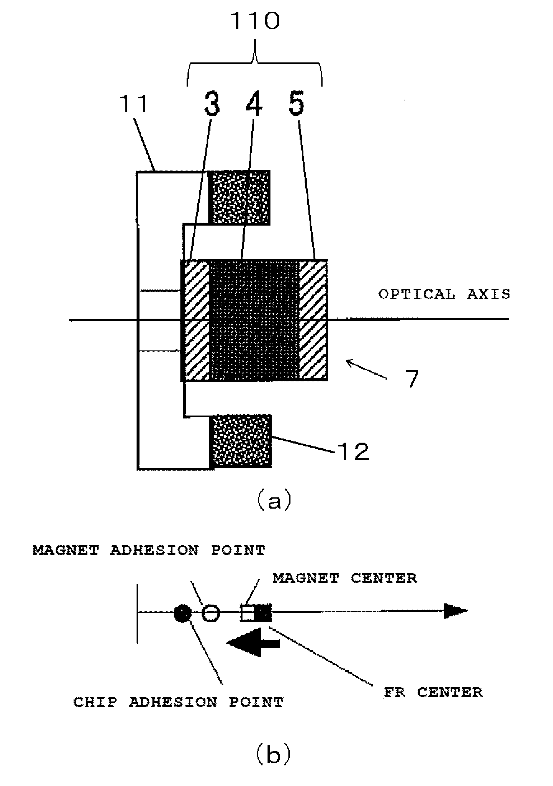
|---|---|---|
| Apr 26, 2016 | JP | 2016-087688 |
Claims
1.-5. (canceled)
6. An optical isolator comprising: an optical isolator chip comprising a first polarizer, a Faraday rotator made of a ferromagnet, and a second polarizer bonded and fixed in this order; and a magnet configured to apply a magnetic field to the optical isolator chip, wherein a light-entering end surface or a light-exiting end surface of the optical isolator chip is bonded and fixed to a component, an end portion of the magnet, which is on the same side as the end surface side of the optical isolator chip bonded and fixed to the component, is bonded and fixed to the component, on an optical axis of the optical isolator, a center of a magnetic flux formed by the magnet is positioned between a central position of the Faraday rotator on the optical axis and the end surface bonded and fixed to the component, and the light-entering end surface or the light-exiting end surface of the optical isolator chip not bonded and fixed to the component protrudes from an end portion of the magnet not bonded and fixed to the component.
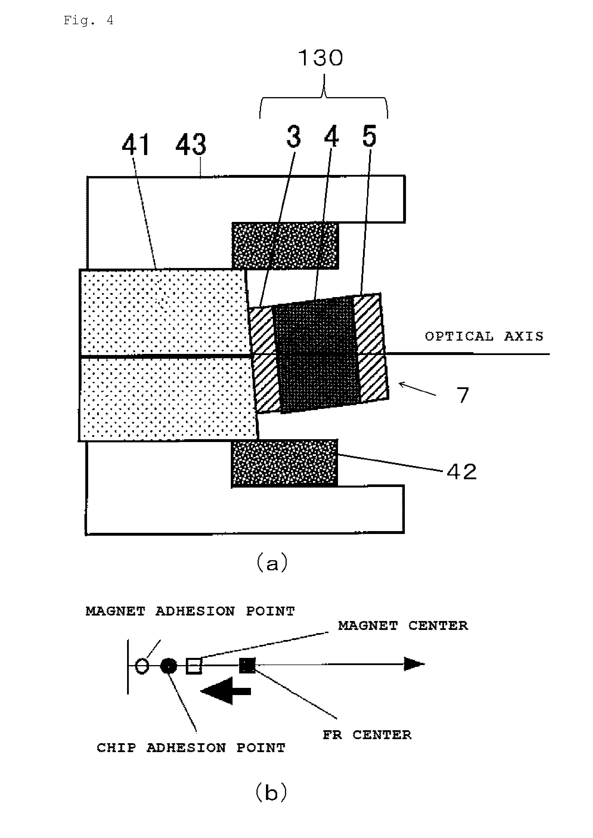
7. The optical isolator according to claim 6, wherein the component bonded and fixed to the optical isolator chip is integrated with a component bonded and fixed to the magnet, so that a single part is formed.
8. The optical isolator according to claim 6, wherein the component bonded and fixed to the optical isolator chip is a stub of a receptacle.
9. The optical isolator according to claim 7, wherein the component bonded and fixed to the optical isolator chip is a stub of a receptacle.
10. The optical isolator according to claim 6, wherein the component bonded and fixed to the magnet is a casing of the receptacle.
11. The optical isolator according to claim 7, wherein the component bonded and fixed to the magnet is a casing of the receptacle.
12. The optical isolator according to claim 8, wherein the component bonded and fixed to the magnet is a casing of the receptacle.
13. The optical isolator according to claim 9, wherein the component bonded and fixed to the magnet is a casing of the receptacle.
Description
TECHNICAL FIELD
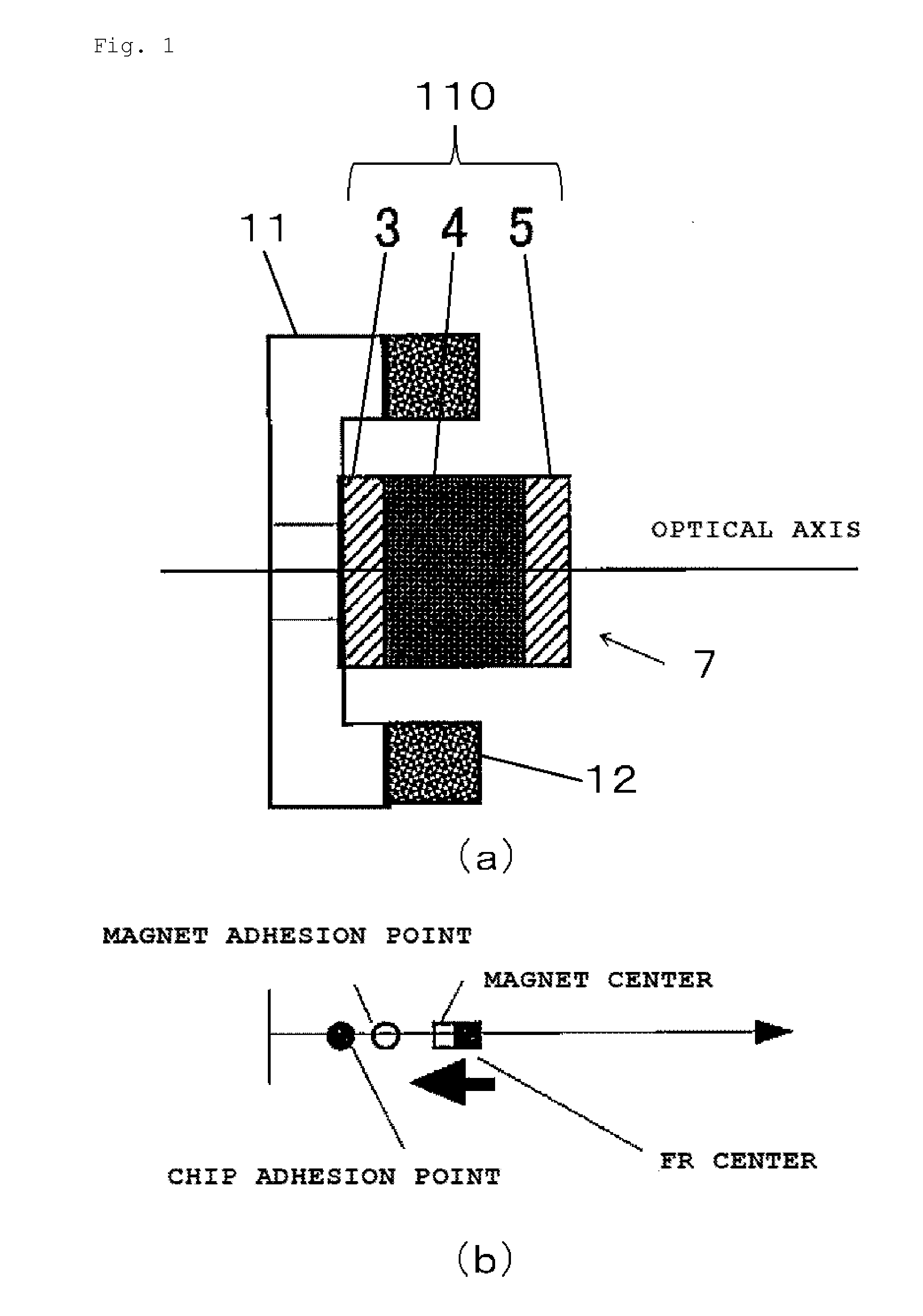
[0001] The present invention relates to an optical isolator which is an optical component used in optical communication and optical measurement to prevent light, which is reflected from a fiber end or a lens end, from returning to a light-source laser.
BACKGROUND ART
[0002] In optical communication and optical measurement, when light emitted from a semiconductor laser returns to the semiconductor laser by reflection at the surface of a component provided in the transmission path, the laser oscillation becomes unstable. To block such reflected return light, an optical isolator using a Faraday rotator which rotates a plane of polarization non-reciprocally is employed (see, for example, Patent Document 1 and so forth).
[0003] An optical isolator is, for example, bonded and fixed to an end surface of a stub and integrated with a receptacle in some cases. The optical isolator with such a configuration is incorporated in a semiconductor laser module or the like for use.
CITATION LIST
Patent Document
[0004] Patent Document 1: Japanese Unexamined Patent Publication (Kokai) No. 2011-150208
SUMMARY OF INVENTION
Technical Problems
[0005] Semiconductor laser modules are required to achieve cost reduction, space saving, weight reduction, and so forth. Similarly, parts constituting such modules are also required to achieve cost reduction, space saving, weight reduction, and so forth.
[0006] Moreover, in preparing semiconductor laser modules, detachment or breakage may occur at the bonding interface between an optical isolator and a component such as a stub due to influences from temperature increase and impact by YAG welding, temperature increase by AuSn solder bonding, or the like.
[0007] The present invention has been accomplished in view of the problems described above. An object of the present invention is to provide an optical isolator which achieves cost reduction, space saving, weight reduction, and high reliability of bonding to a component even under influences such as thermal expansion, in comparison with conventional products.
Solution to Problems
[0008] To achieve the above object, the present invention provides an optical isolator comprising:
[0009] an optical isolator chip comprising a first polarizer, a Faraday rotator made of a ferromagnet, and a second polarizer bonded and fixed in this order; and
[0010] a magnet configured to apply a magnetic field to the optical isolator chip, wherein
[0011] a light-entering end surface or a light-exiting end surface of the optical isolator chip is bonded and fixed to a component, and
[0012] on an optical axis of the optical isolator, a center of a magnetic flux formed by the magnet is positioned closer to the end surface side bonded and fixed to the component than a central position of the Faraday rotator on the optical axis is.
[0013] With this structure where the center of a magnetic flux formed by the magnet is positioned closer to the end surface side of the optical isolator chip bonded and fixed to the component than the central position of the Faraday rotator on the optical axis is, a force for pressing the optical isolator chip against the component is exerted, enabling an optical isolator having high reliability of bonding to the component. In addition, the magnet is made so compact that the optical isolator achieves cost reduction, space saving, and weight reduction.
[0014] In this situation, an end portion of the magnet, which is located on the same side as the end surface side of the optical isolator chip bonded and fixed to the component, may be bonded and fixed to the component.
[0015] In this way, when bonding and fixing the component to the end portions of the optical isolator chip and the magnet located on the same side simplifies the structure of the component to which the optical isolator is attached, and can further enhance the bonding reliability of the optical isolator.
[0016] In this situation, the component bonded and fixed to the optical isolator chip is preferably integrated with a component bonded and fixed to the magnet, so that a single part is formed.
[0017] When the optical isolator chip and the magnet are bonded and fixed to such components integrated to form a single part, the part formed therefrom can be easily produced, and such parts are applicable to various usages.
[0018] In this situation, the component bonded and fixed to the optical isolator chip can be a stub of a receptacle.
[0019] In this way, when the optical isolator chip and such a stub of a receptacle are bonded and fixed to each other, this can simplify the structure of the receptacle and further enhance the bonding reliability of the optical isolator.
[0020] In this situation, the component bonded and fixed to the magnet can be a casing of the receptacle.
[0021] In this way, when the optical isolator chip and such a casing of a receptacle are bonded and fixed to each other, this can simplify the structure of the receptacle and further enhance the bonding reliability of the optical isolator.
Advantageous Effects of Invention
[0022] The present invention makes it possible to provide an optical isolator which achieves high bonding reliability, cost reduction, space saving, and light weight, in comparison with conventional products.
BRIEF DESCRIPTION OF DRAWINGS
[0023] FIG. 1 shows a schematic drawing illustrating an example of an optical isolator of the present invention (FIG. 1(a)), and a schematic diagram illustrating a relation between a center of a Faraday rotator and a center of a magnetic flux (magnet center) (FIG. 1(b)) (Example 1).
[0024] FIG. 2 shows a schematic drawing illustrating another example of the inventive optical isolator (FIG. 2(a)), and a schematic diagram illustrating a relation between the center of the Faraday rotator and the center of the magnetic flux (magnet center) (FIG. 2(b)) (Example 2).
[0025] FIG. 3 shows a schematic drawing illustrating still another example of the inventive optical isolator (FIG. 3(a)), and a schematic diagram illustrating a relation between the center of the Faraday rotator and the center of the magnetic flux (magnet center) (FIG. 3(b)) (Example 3).
[0026] FIG. 4 shows a schematic drawing illustrating still another example of the inventive optical isolator (FIG. 4(a)), and a schematic diagram illustrating a relation between the center of the Faraday rotator and the center of the magnetic flux (magnet center) (FIG. 4(b)) (Example 4).
[0027] FIG. 5 shows a schematic drawing illustrating an example of a conventional optical isolator (FIG. 5(a)), and a schematic diagram illustrating a relation between a center of a Faraday rotator and a center of a magnetic flux (magnet center) (FIG. 5(b)).
DESCRIPTION OF EMBODIMENTS
[0028] Hereinafter, exemplary embodiments of the present invention will be explained in detail with reference to the drawings, but the present invention is not limited thereto.
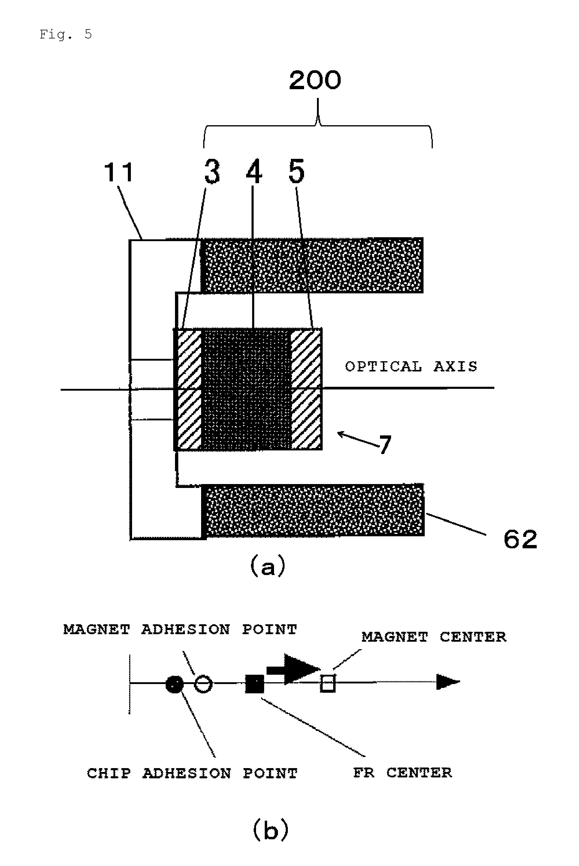
[0029] FIG. 5(a) is a schematic drawing illustrating a conventional optical isolator. This optical isolator 200 has: an optical isolator chip 7 including a first polarizer 3, a Faraday rotator 4 made of a ferromagnet, and a second polarizer 5 bonded and fixed in this order; and a magnet 62 configured to apply a magnetic field to the optical isolator chip 7. This magnet 62 has a cylindrical shape and surrounds the optical isolator chip 7. In the optical isolator 200, a left end (light-entering end surface or light-exiting end surface) of the optical isolator chip 7 and a left end of the magnet 62 are each bonded and fixed to a metal holder 11.
[0030] The optical axis of the optical isolator 200 coincides with the central axis of the cylindrical magnet 62. A magnetic flux is formed between right and left end portions of the magnet 62, and the center of the magnetic flux on the optical axis is defined as magnet center. FIG. 5(b) illustrates a relation between the center of the magnetic flux (magnet center) and a central position of the Faraday rotator 4 (hereinafter, indicated as FR center in the drawing) on the optical axis in the conventional optical isolator 200 bonded and fixed to the component (the metal holder 11). In the conventional optical isolator 200, the center of the magnetic flux (magnet center) is positioned at a right side of the central position of the Faraday rotator 4 on the optical axis, that is, at a side opposite to the end surface side bonded to the metal holder 11. Moreover, FIG. 5(b) also shows a point where the magnet 62 adheres to the metal holder 11 (indicated as magnet adhesion point in the drawing) and a point where the optical isolator chip 7 adheres to the metal holder 11 (indicated as chip adhesion point in the drawing).
[0031] A magnetic force from the magnet 62 acts on the Faraday rotator 4 placed in the magnetic field formed by the magnet 62. A force toward the center of the magnetic flux (magnet center) acts on the central position of the Faraday rotator 4 on the optical axis. Specifically, in the structure shown in FIG. 5(a), a force for separating the metal holder 11 and the optical isolator chip 7 is exerted (see the bold arrow in FIG. 5(b)). Hence, detachment or breakage is likely to occur between the metal holder 11 and the optical isolator chip 7. Additionally, when the optical isolator 200 is placed in a high-temperature environment, an adhesive for adhering the optical isolator chip 7 to the metal holder 11 is softened, so that the fixation becomes unstable, and a stress is generated at the bonded portion due to a difference in thermal expansion coefficient between the materials, for example, so that the detachment or breakage is particularly likely to occur.
[0032] Next, a configuration of an optical isolator of the present invention will be explained below with reference to a schematic drawing (FIG. 1(a)) illustrating an example of the inventive optical isolator and a schematic diagram (FIG. 1(b)) illustrating a relation between a center of a Faraday rotator and a center of a magnetic flux (magnet center).
[0033] The inventive optical isolator 110 shown in FIG. 1(a) has: an optical isolator chip 7 including a first polarizer 3, a Faraday rotator 4 made of a ferromagnet, and a second polarizer 5 bonded and fixed in this order; and a magnet 12 configured to apply a magnetic field to the optical isolator chip 7. A light-entering end surface or a light-exiting end surface of the optical isolator chip 7 is bonded and fixed to a metal holder 11. Moreover, as shown in FIG. 1(b), on an optical axis of the optical isolator 110, the center of a magnetic flux (magnet center) formed by the magnet 12 is positioned closer to the end surface side bonded and fixed to the metal holder 11 than the central position of the Faraday rotator 4 on the optical axis (FR center) is.
[0034] With such a structure that the center of the magnetic flux (magnet center) is positioned closer to the bonded- and fixed-end surface side of the optical isolator chip 7 than the central position of the Faraday rotator 4 on the optical axis is, a force for pressing the optical isolator chip 7 against the metal holder 11 is constantly exerted (see the bold arrow in FIG. 1(b)). This enables the optical isolator 110 to have quite high bonding reliability to the component (the metal holder 11). Moreover, it is also possible to shorten the magnet dimensions, so that the cost reduction, space saving, and weight reduction can be achieved.
[0035] The force acting on the center of the Faraday rotator 4 is determined by the balance of forces acting on the Faraday rotator 4 in right and left directions in FIG. 1(a). In the case where the center of the magnetic flux (magnet center) coincides with the central position of the Faraday rotator 4 on the optical axis, the forces acting in the right and left directions are almost equal to each other, so that forces hardly act in any of the right and left directions. In other words, in a case where the center of the magnetic flux (magnet center) does not coincide with the central position of the Faraday rotator 4 on the optical axis, a force is exerted such that the central position of the Faraday rotator 4 on the optical axis comes close to the center of the magnetic flux (magnet center). The above-described force for pressing the optical isolator chip 7 against the metal holder 11 is such a force.
[0036] In addition, an end portion of the magnet 12, which is located on the same side as the end surface side of the optical isolator chip 7 bonded and fixed to the metal holder 11, may be bonded and fixed to the metal holder 11. In this way, when the end portions of the optical isolator chip 7 and the magnet 12 located on the same side are bonded and fixed to the metal holder 11, this makes it possible to simplify the structure of the component attached to the optical isolator 110, and to further enhance the bonding reliability (bonding stability) of the optical isolator.
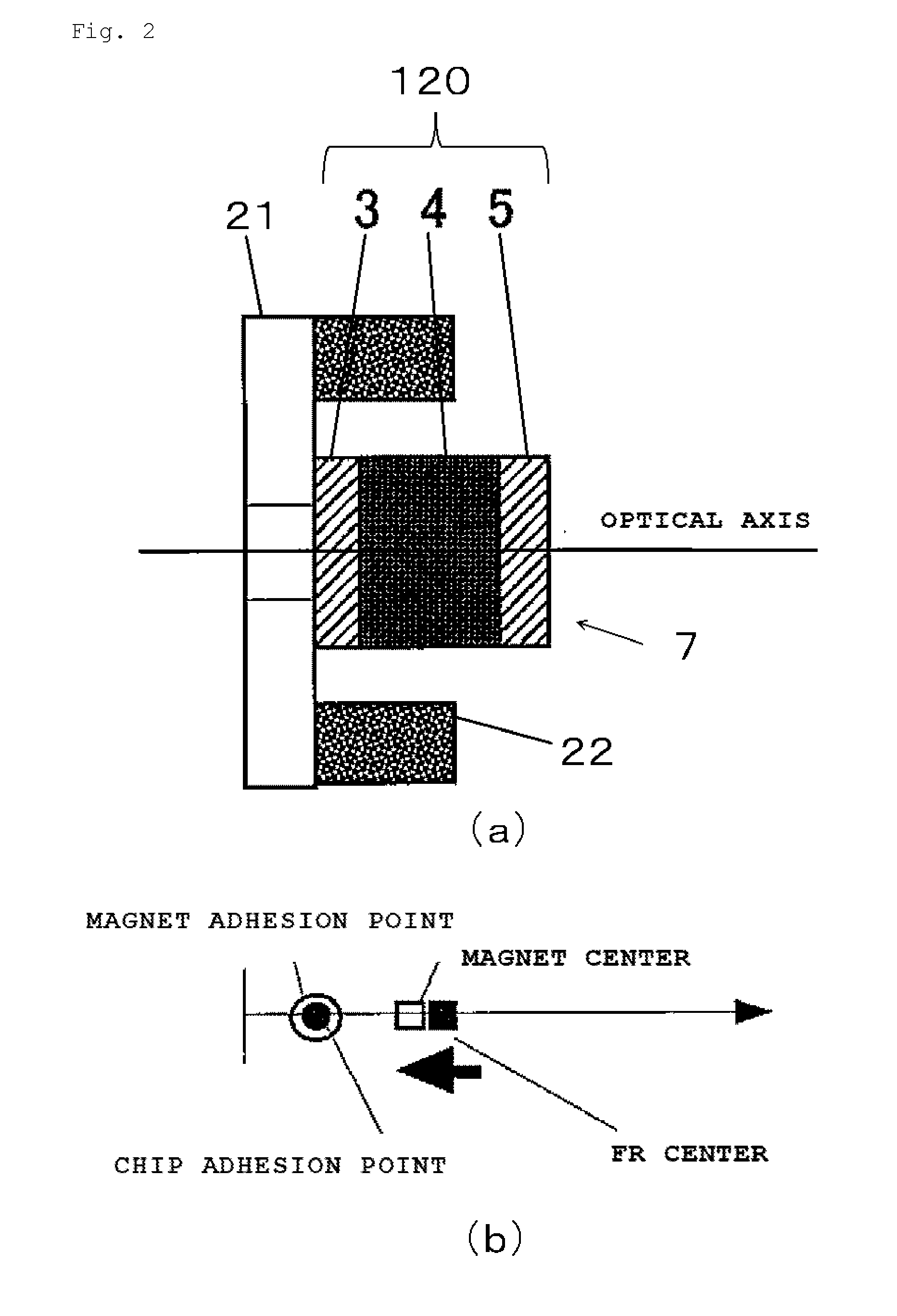
[0037] In the inventive optical isolator 110 described with reference to FIG. 1, the optical isolator chip 7 and the magnet 12 are bonded and fixed to the same component. Nevertheless, the present invention is not limited thereto. As shown in FIG. 3(a), the optical isolator chip 7 and the magnet 12 can also be bonded and fixed to components which are integrated to form a single part. For example, the component bonded and fixed to the optical isolator chip may be a stub of a receptacle, while the component bonded and fixed to the magnet may be a casing of the receptacle.
[0038] Specifically, a schematic drawing as shown in FIG. 3(a) illustrates another example of the above-described inventive optical isolator, and FIG. 3(b) is a schematic diagram illustrating a relation between the center of the Faraday rotator and the center of the magnetic flux (magnet center). In the embodiment shown in FIG. 3(a), the component bonded and fixed to the optical isolator chip 7 can be a stub 31 of a receptacle. Meanwhile, the component bonded and fixed to a magnet 32 can be a casing 33 of the receptacle. Such a structure can simplify the structure of the receptacle, and further enhance the bonding reliability of an optical isolator 130.
[0039] Additionally, in FIG. 3(a) also, the center of the magnetic flux (magnet center) is positioned closer to the bonded- and fixed-end surface side of the optical isolator chip 7 than the central position of the Faraday rotator 4 on the optical axis is. Hence, as shown in FIG. 3(b), a force for pressing the optical isolator chip 7 (the Faraday rotator 4) against the stub 31 of the receptacle is exerted, and enhances the bonding reliability of the optical isolator.
EXAMPLES
[0040] Hereinafter, the present invention will be more specifically described by showing Examples and Comparative Examples, but the present invention is not limited thereto.
Example 1
[0041] The optical isolator shown in FIG. 1(a) was produced as follows. First, (TbEu).sub.2Bi.sub.1Fe.sub.4.8Ga.sub.0.2O.sub.12 was used as the Faraday rotator 4, and polished (length: 0.60 mm) to have a Faraday rotation angle of 45 degrees at 25.degree. C. for light having 1550 nm wavelength. Further, AR coating films against epoxy were formed on both end surfaces of the Faraday rotator 4.
[0042] Next, polarizing glasses (the second polarizer 5, the first polarizer 3) having AR coating films against air formed at a light-entering surface side and a light-exiting surface side were prepared, and bonded and fixed to the Faraday rotator 4 with an epoxy adhesive. This assembly was cut into a 0.8-mm square (having a squared cross section with each side of 0.8 mm). Thus, the optical isolator chip 7 was prepared.
[0043] Then, the light-exiting end surface of the optical isolator chip 7 and the SmCo magnet 12 (outer diameter: 2 mm, inner diameter: 1.3 mm, length: 0.4 mm) were adhered and fixed to the metal holder (first component) 11 to produce the optical isolator 110. In this case, as shown in FIG. 1(b), the center of the magnetic flux (magnet center) formed by the magnet 12 on the optical axis was positioned closer to the light-exiting end surface side (left side) than the central position of the Faraday rotator 4 on the optical axis (FR center) was. Moreover, the forward insertion loss of the produced optical isolator 110 was 0.14 dB, and the isolation was 43 dB.
[0044] In the optical isolator 110 of Example 1, the weight, volume, and cost of the magnet were each reduced to approximately 4/15 of those of a magnet in an optical isolator of Comparative Example 1 (to be described later).
[0045] Further, in the step of incorporating the optical isolator 110 into a laser module, even when 1 hour elapsed at a temperature of 260.degree. C., no abnormality was observed at the adhesion portion between the optical isolator chip 7 and the metal holder 11.
Example 2
[0046] The optical isolator shown in FIG. 2(a) was produced as follows. First, the optical isolator chip 7 was produced as in Example 1. Then, the light-exiting end surface of the optical isolator chip 7 and a SmCo magnet 22 (outer diameter: 2 mm, inner diameter: 1.3 mm, length: 0.6 mm) were adhered and fixed to a disc-shaped metal holder (second component) 21 to produce an optical isolator 120 as in Example 1. In Example 2, the shape of the metal holder and the size of the SmCo magnet differ from those in Example 1.
[0047] In this case, as shown in FIG. 2(b), the center of the magnetic flux formed by the magnet 22 on the optical axis was positioned closer to the light-exiting end surface side (left side) than the central position of the Faraday rotator 4 on the optical axis (FR center) was. Moreover, the forward insertion loss of the produced optical isolator 120 was 0.16 dB, and the isolation was 42 dB.
[0048] In the optical isolator 120 of Example 2, the weight, volume, and cost of the magnet were each reduced to approximately 6/15 of those of the magnet in the optical isolator of Comparative Example 1 to be described later.
[0049] Further, in the step of incorporating the optical isolator 120 into a laser module, even when 1 hour elapsed at a temperature of 260.degree. C., no abnormality was observed at the adhesion end portion between the optical isolator chip 7 and the disc-shaped metal holder 21.
Example 3
[0050] The optical isolator shown in FIG. 3(a) was produced as follows. First, the optical isolator chip 7 was produced as in Example 1. Then, the light-exiting end surface of the optical isolator chip 7 was adhered and fixed to the stub (third component) 31 of the receptacle, and the SmCo magnet 32 (outer diameter: 2 mm, inner diameter: 1.3 mm, length: 0.8 mm) was adhered and fixed to the receptacle casing (fourth component) 33 to produce the optical isolator 130. Example 3 differs from Examples 1 and 2 in that the component bonded and fixed to the optical isolator chip 7 and the component bonded and fixed to the magnet 32 were integrated to form a single part, and that the end surface of the component (the stub 31) bonded and fixed to the optical isolator chip 7 is tilted away from the optical axis.
[0051] In this case, as shown in FIG. 3(b), the center of the magnetic flux formed by the magnet 32 on the optical axis was positioned closer to the light-exiting end surface side (left side) than the central position of the Faraday rotator 4 on the optical axis (FR center) was. Moreover, the forward insertion loss of the produced optical isolator 130 was 0.15 dB, and the isolation was 43 dB.
[0052] In the optical isolator 130 of Example 3, the weight, volume, and cost of the magnet were each reduced to approximately 8/15 of those of the magnet in the optical isolator of Comparative Example 1.
[0053] Further, in the step of incorporating the optical isolator 130 into a laser module, even when 10 hours elapsed at a temperature of 150.degree. C., no abnormality was observed at the adhesion portion between the optical isolator chip 7 and the stub 31.
Example 4
[0054] As shown in FIG. 4(a), in this Example, one end of a casing 43 of a receptacle was extended such that the light-entering end surface of the optical isolator chip 7 did not protrude outwardly from the magnet and the position of the end surface of the component, as compared with the optical isolator 130 of Example 3 shown in FIG. 3(a). The SmCo magnet 42 was the same as the SmCo magnet 32, and a stub 41 of the receptacle was the same as the stub 31 of the receptacle.
[0055] This makes it possible to avoid a possibility of a crack or the like which would be otherwise formed in the end surface of the optical isolator chip 7 abutting on a lens casing or the like during the incorporation into a laser module.
Comparative Example 1
[0056] The optical isolator shown in FIG. 5(a) was produced as follows. First, (TbEu).sub.2Bi.sub.1Fe.sub.4.8Ga.sub.0.2O.sub.12 was used as the Faraday rotator 4, and polished (length: 0.60 mm) to have a Faraday rotation angle of 45 degrees at 25.degree. C. for light having 1550 nm wavelength. Further, AR coating films against epoxy were formed on both end surfaces of the Faraday rotator 4.
[0057] Next, polarizing glasses (the second polarizer 5, the first polarizer 3) having AR coating films against air formed at a light-entering surface side and a light-exiting surface side were prepared, and bonded and fixed to the Faraday rotator 4 with an epoxy adhesive. This assembly was cut into a 0.8-mm square. Thus, the optical isolator chip 7 was prepared.
[0058] Then, the light-exiting end surface of the optical isolator chip 7 and the SmCo magnet 62 (outer diameter: 2 mm, inner diameter: 1.3 mm, length: 1.5 mm) were adhered and fixed to the metal holder 11 to produce the optical isolator 200. In the structure of this case, the light-entering end surface of the optical isolator chip 7 generally does not protrude from the end portion of the magnet 62 not bonded and fixed to the metal holder 11. Moreover, the center of the magnetic flux (magnet center) formed by the magnet 62 on the optical axis was positioned at the light-entering end surface side (right side) of the central position of the Faraday rotator 4 on the optical axis (FR center). Further, the forward insertion loss of the produced optical isolator 200 was 0.15 dB, and the isolation was 42 dB.
[0059] In the step of incorporating the optical isolator 200 into a laser module, when 10 hours elapsed at a temperature of 150.degree. C., the adhesion portion between the optical isolator chip 7 and the metal holder 11 broke and detached.
[0060] This is conceivably because when the optical isolator 200 became so hot that the epoxy adhesive was softened, a force in a direction of the center of the magnetic flux (magnet center) acted on the Faraday rotator 4 made of a magnetic material (see FIG. 5(b)).
[0061] In addition, since the weight and volume of the magnet in Comparative Example 1 were greater than those of Examples 1 to 4, it was difficult to make an optical isolator compact (saving space, light weight) and reduce the cost.
[0062] It should be noted that the present invention is not restricted to the above-described embodiments. The embodiments are merely examples so that any embodiments that have substantially the same feature and demonstrate the same functions and effects as those in the technical concept as disclosed in claims of the present invention are included in the technical scope of the present invention.
* * * * *
D00000
D00001
D00002
D00003
D00004
D00005
XML
uspto.report is an independent third-party trademark research tool that is not affiliated, endorsed, or sponsored by the United States Patent and Trademark Office (USPTO) or any other governmental organization. The information provided by uspto.report is based on publicly available data at the time of writing and is intended for informational purposes only.
While we strive to provide accurate and up-to-date information, we do not guarantee the accuracy, completeness, reliability, or suitability of the information displayed on this site. The use of this site is at your own risk. Any reliance you place on such information is therefore strictly at your own risk.
All official trademark data, including owner information, should be verified by visiting the official USPTO website at www.uspto.gov. This site is not intended to replace professional legal advice and should not be used as a substitute for consulting with a legal professional who is knowledgeable about trademark law.