Quantum Confined Stark Effect Electroabsorption Modulator On A Soi Platform
YU; Guomin ; et al.
U.S. patent application number 16/315510 was filed with the patent office on 2019-08-01 for quantum confined stark effect electroabsorption modulator on a soi platform. The applicant listed for this patent is POLITECNICO DI MILANO, ROCKLEY PHOTONICS LIMITED. Invention is credited to Andrea BALLABIO, Jacopo FRIGERIO, Giovanni ISELLA, Guomin YU.
| Application Number | 20190235286 16/315510 |
| Document ID | / |
| Family ID | 58410409 |
| Filed Date | 2019-08-01 |


View All Diagrams
| United States Patent Application | 20190235286 |
| Kind Code | A1 |
| YU; Guomin ; et al. | August 1, 2019 |
QUANTUM CONFINED STARK EFFECT ELECTROABSORPTION MODULATOR ON A SOI PLATFORM
Abstract
An electroabsorption modulator. The modulator comprising an SOI waveguide; an active region, the active region comprising a multiple quantum well (MQW) region; and a coupler for coupling the SOI waveguide to the active region. The coupler comprising: a transit waveguide coupling region; a buffer waveguide coupling region; and a taper region; wherein, the transit waveguide coupling region couples light between the SOI waveguide and the buffer waveguide coupling region; and the buffer waveguide coupling region couples light between the transit waveguide region and the active region via the taper region.
| Inventors: | YU; Guomin; (Glendora, CA) ; ISELLA; Giovanni; (Como, IT) ; FRIGERIO; Jacopo; (Lecco, IT) ; BALLABIO; Andrea; (Dolzago, IT) | ||||||||||
| Applicant: |
|
||||||||||
|---|---|---|---|---|---|---|---|---|---|---|---|
| Family ID: | 58410409 | ||||||||||
| Appl. No.: | 16/315510 | ||||||||||
| Filed: | January 16, 2017 | ||||||||||
| PCT Filed: | January 16, 2017 | ||||||||||
| PCT NO: | PCT/IT2017/000004 | ||||||||||
| 371 Date: | January 4, 2019 |
Related U.S. Patent Documents
| Application Number | Filing Date | Patent Number | ||
|---|---|---|---|---|
| 62359595 | Jul 7, 2016 | |||
| Current U.S. Class: | 1/1 |
| Current CPC Class: | G02B 6/14 20130101; G02F 1/01708 20130101; G02F 1/01725 20130101; G02F 1/01716 20130101; G02B 6/1228 20130101; B82Y 20/00 20130101; G02F 2001/0157 20130101 |
| International Class: | G02F 1/017 20060101 G02F001/017 |
Claims
1. An electroabsorption modulator comprising: an SOI waveguide; an active region, the active region comprising a multiple quantum well (MQW) region; and a coupler for coupling the SOI waveguide to the active region; the coupler comprising: a transit waveguide coupling region; a buffer waveguide coupling region; and a taper region; wherein, the transit waveguide coupling region couples light between the SOI waveguide and the buffer waveguide coupling region; and the buffer waveguide coupling region couples light between the transit waveguide region and the active region via the taper region.
2. The electroabsorption modulator of claim 1, wherein the taper region comprises a multi-segment mode expander.
3. The electroabsorption modulator of claim 1, wherein the multiple quantum well region is a Ge/SiGe multiple quantum well region.
4. The electroabsorption modulator of claim 1, wherein: the transit waveguide coupling region comprises a first portion of a transit waveguide; and the buffer waveguide coupling region comprises a buffer waveguide located on top of a second portion of the transit waveguide.
5. The electroabsorption modulator of claim 4, wherein: the transit waveguide has a refractive index bigger than that of the SOI waveguide but smaller than that of the buffer waveguide.
6. The electroabsorption modulator of claim 1, wherein: the SOI waveguide is a 3 .mu.m waveguide; the transit waveguide has a thickness of no more than 400 nm; and the buffer waveguide has a thickness of no more than 400 nm.
7. The electroabsorption modulator of claim 6, wherein the transit buffer waveguide has a thickness of no more than 600 nm.
8. The electroabsorption modulator of claim 6, wherein the transit waveguide has a thickness of no more than 800 nm.
9. The electroabsorption modulator of claim 1, wherein each of the buffer waveguide and transit waveguide are SiGe waveguides.
10. The electroabsorption modulator of claim 4; wherein the active region comprises: a P-doped region between the buffer layer and the lower surface of a spacer layer underneath a multiple quantum well; and an N-doped region located at the upper surface of a spacer layer on top of the multiple quantum well.
11. The electroabsorption modulator of claim 10, further comprising multiple N-type doped layers with different germanium compositions and doping concentrations.
12. The electroabsorption modulator of claim 1, wherein the waveguide slab of the P-type layer in the active region is P-doped with ion implantation followed by an RTA process.
13. The electroabsorption modulator of claim 1, wherein the electrodes are arranged in a ground-signal (GS) configuration, where a ground electrode is located at an opposite side of the active region from the signal electrode.
14. The electroabsorption modulator of claim 1, wherein the electrodes are arranged in a ground-signal-ground (GSG) configuration, where a first ground electrode and a second ground electrode are located at the same side of the active region as the signal electrode.
15. The electroabsorption modulator of claim 1, wherein the multiple quantum well region includes at least 5 quantum wells.
16. The electroabsorption modulator of claim 1, wherein the multiple quantum well region includes either 5, 7, or 10 quantum wells.
17. The electroabsorption modulator of claim 1, wherein the multiple quantum well region is no more than 240 nm thick, and is preferably no more than 232 nm thick.
18. The electroabsorption modulator of claim 1, wherein a spacing between respective pairs of the quantum wells is in the range of 10 nm to 20 nm.
19. The electroabsorption modulator of claim 1, wherein each of the multiple quantum wells has a thickness in the range of 5 nm to 15 nm.
20. The electroabsorption modulator of claim 1, further comprising a metal electrode in contact with a surface of the active region opposite to the coupler, wherein the MQW region includes at least one tapered portion of MQW material which extends into the taper region; and wherein the metal electrode extends as far as the tapered portion of MQW material.
21. The electroabsorption modulator of claim 20, wherein the electrode has a length in the direction towards the taper region which is greater than 2.5 .mu.m.
22. The electroabsorption modulator of claim 1, wherein the active region includes an N-doped region located above the upper surface of a spacer layer on top of the multiple quantum well region, and wherein the N-doped region comprises Si.sub.0.9Ge.sub.0.1.
Description
FIELD
[0001] The present invention relates to a modulator and to optical coupling within a modulator on an SOI platform and more particularly to a SiGe quantum confined Stark effect (QCSE) modulator.
BACKGROUND
[0002] It is desirable to make high speed SiGe quantum confined Stark effect (QCSE) electroabsorption modulators (EAMs) operating at O-band (1.3 .mu.m wavelength) and CMOS compatible on SOI platform for data centre network applications. Due to the limitation of germanium material properties (bandgap and absorption), problems to make SiGe QCSE EAM operate at O-band on 3 .mu.m SOI platform include 1) the design of SiGe multiple quantum well epitaxy (EPI) stack that can operate at 1.3 .mu.m wavelength; 2) the design of coupling structure that brings the light from 3 .mu.m SOI waveguide into the SiGe multiple quantum well (MQW) waveguide with low loss based on the EPI structure due to large SOI waveguide dimensions and big refractive index contrast between Si and SiGe buffer layer for the SiGe MQW; and 3) the difficulty of realizing 2V driving voltage with CMOS driver because of the carrier screen effect in the MQW region. This invention aims to overcome at least these three problems in making SiGe QCSE EAM on 3 .mu.m SOI platform.
[0003] Whilst this application focusses on coupling to 3 .mu.m SOI waveguides, it should be understood that the physical structures described herein could be scaled up or scaled down in size accordingly to other sizes of waveguides.
SUMMARY
[0004] According to a first aspect, the invention provides an electroabsorption modulator comprising: an SOI waveguide; an active region, the active region comprising a multiple quantum well (MQW) region; and a coupler for coupling the SOI waveguide to the active region; the coupler comprising: a transit waveguide coupling region; a buffer waveguide coupling region; and a taper region; wherein, the transit waveguide coupling region couples light between the SOI waveguide and the buffer waveguide coupling region; and the buffer waveguide coupling region couples light between the transit waveguide region and the active region via the taper region.
[0005] Here are presented a SiGe MQW EPI stack based on 3 .mu.m SOI wafer and an electroabsorption modulator (EAM) based on the SiGe EPI stack. The SiGe MQW EPI stack is designed such that it can: 1) realize operating in O-band (1.3 .mu.m wavelength); 2) fulfil 2V driving voltage for QCSE EAM that is compatible with CMOS drivers by properly choosing the quantum well structure with low optical loss; and 3) support the design of coupling structure to bring light from 3 .mu.m SOI waveguide to the SiGe MQW active region. The SiGe EPI stack comprises (from bottom to top): a transit buffer layer that is for the first evanescent coupling structure to bring light up from the 3 .mu.m SOI waveguide; a buffer layer that serves as the virtual substrate to determine the strain in the well layer and barrier layer in the SiGe MQW, as well as the second evanescent coupling structure to bring light up from the transit buffer layer to the SiGe MQW active region through a taper structure (mode expander); a P-type (e.g. boron) doped layer that acts as the P-side of the PIN junction in the SiGe EAM with a concentration of 1E18 cm.sup.-3; an intrinsic spacer layer that separates the P-type doped layer and the SiGe quantum wells; a layer of five SiGe quantum wells that comprise five germanium wells and six SiGe barriers--the number of quantum wells should be chosen such that with a 2V driving voltage an extinction ratio of 4 dB or bigger may be achieved at 1.3 .mu.m; an intrinsic spacer layer to separate the quantum wells and the N-type doped layers, a layer of N-type (e.g. phosphorus) doped with a concentration of 1E18 cm.sup.-3 and the same germanium composition as the P-type doped layer; a layer of N-type doped with a concentration of 1E18 cm.sup.-3 but a lower germanium composition; a layer of heavily N-type doped with a concentration of 1E20 cm.sup.-3 and the same germanium composition as the last N-type doped layer. The use of multiple N-type doped layers with different germanium composition and different doping concentrations is to realize both low optical loss and low series resistance to reach high modulation speed.
[0006] The SiGe QCSE EAM comprises: an SOI waveguide; an active region, the active region comprising a SiGe multiple quantum well waveguide; and two coupling regions, the coupling region has at least one evanescent coupling and one taper structure to couple light between the SOI waveguide and the SiGe MQW waveguide active region. The SOI waveguide has a typical thickness of 3 .mu.m and a typical width of 2.6 .mu.m based on 3 .mu.m SOI wafers. The evanescent coupling structures in the coupling region comprises a transit buffer layer waveguide and a buffer layer waveguide on top of the transit buffer layer waveguide. The light from the 3 .mu.m SOI waveguide is coupled into the transit buffer layer waveguide first; then the light is coupled into the buffer layer waveguide which may comprise the buffer layer itself only or comprise the buffer layer with the P-type doped layer together; then the light is coupled into the SiGe MQW waveguide via a taper that comprises the transit buffer layer, buffer layer, P-type doped layer, spacer layer, SiGe MQW layers, spacer layer and N-type doped layers. The taper structure is designed such that it expands the optical mode of the buffer waveguide to the optical mode of the SiGe MQW waveguide with low optical loss and minimizes the extra parasitical capacitance to keep the EAM working at high speed. In the active region, the SiGe waveguide is a rib waveguide with the P-type doped layer on top of the slab, on which the metal electrode is deposited. In order to reduce the contact resistance between the metal electrode and the P-type doped layer, an ion implantation is used to make it heavily P-type (e.g. boron) doped followed by a rapid thermal annealing (RTA) process to activate the dopant. The doped concentration is about 1E20 cm.sup.-3. The electrode on the N-side of the PIN junction of the SiGe EAM contacts the heavily doped N-type layer from the top of the waveguide with the bonding pad on the waveguide slab. In order to reduce the parasitical capacitance, the part of P-type doped layer on the waveguide slab underneath the electrode and the bonding pad for the N-type layer has to be removed. Two kinds of electrode pad arrangements have been used. One arrangement is ground-signal (GS), and the other is ground-signal-ground (GSG). In the GS configuration, a ground electrode is located at an opposite side of the active region from the signal electrode. In a ground-signal-ground (GSG) configuration, a first ground electrode and a second ground electrode are located at the same side of the active region as the signal electrode. The active region may be an active region waveguide. In embodiments of this invention, light is efficiently coupled from 3 .mu.m SOI waveguide to SiGe multiple quantum well (MQW) waveguide, where the light is modulated, then is coupled back to the 3 .mu.m SOI waveguide. This overcomes the inherent problems which arise due to an SOI waveguide having relatively large dimensions and refractive index contrast between Si and the SiGe buffer layer for the SiGe MQW waveguide.
[0007] The taper region may comprise a multi-segment mode expander.
[0008] The multiple quantum well region may be a Ge/SiGe multiple quantum well region
[0009] The transit waveguide coupling region may comprise a first portion of a transit waveguide; and the buffer waveguide coupling region comprises a buffer waveguide located on top of a second portion of the transit waveguide.
[0010] Optionally, the transit buffer layer has a refractive index bigger than that of the SOI waveguide but smaller than that of the buffer layer.
[0011] Optionally, the SOI waveguide is a 3 .mu.m waveguide; the transit buffer layer has a thickness of no more than 400 nm; and the buffer layer has a thickness of no more than 400 nm.
[0012] Optionally, the transit buffer layer has a thickness of no more than 600 nm.
[0013] Optionally, the transit buffer layer has a thickness of no more than 800 nm.
[0014] Optionally, each of the buffer layer and transit buffer layer are SiGe waveguides.
[0015] The active region may comprise: a P-doped region between the buffer layer and the lower surface of a spacer layer underneath a multiple quantum well; and an N-doped region located at the upper surface of a spacer layer on top of the multiple quantum wells.
[0016] The modulator may further comprise multiple N-type doped layers with different germanium compositions and doping concentrations.
[0017] The waveguide slab of the P-type layer in the active region may be P-doped with ion implantation followed by an RTA process.
[0018] The electrodes may be arranged in a ground-signal (GS) configuration, where a ground electrode is located at an opposite side of the active region from the signal electrode.
[0019] The electrodes may be arranged in a ground-signal-ground (GSG) configuration, where a first ground electrode and a second ground electrode are located at the same side of the active region as the signal electrode.
[0020] The multiple quantum well region may include at least 5 quantum wells. The multiple quantum well region may include either 5, 7, or 10 quantum wells.
[0021] The multiple quantum well region may be no more than 240 nm thick, and is preferably no more than 232 nm thick.
[0022] The modulator may further comprise a metal electrode in contact with a surface of the active region opposite to the coupler, the metal electrode may extend beyond the active region in a direction towards the taper region. The electrode may have a length in the direction towards the taper region which is greater than 2.5 .mu.m. Whilst the active region includes the MQW region, the MQW region may extend beyond a length of the main body of the active region i.e. the MQW region may be coterminous with the spacer layer discussed above. In this way, the MQW region may include at least one tapered portion of MQW material which extends into the taper region; and wherein the metal electrode extends beyond the active region in a direction towards the taper region as far as the tapered portion of MQW material.
[0023] The active region may include an N-doped region located above the upper surface of a spacer layer on top of the multiple quantum well region, and the N-doped region may comprise Si.sub.0.9Ge.sub.0.1.
[0024] The active region may include one or more angled interfaces, which are angled relative to the wave-guiding direction of the SOI waveguide. The angled interfaces may be formed by the interfaces between the stack and an input and output waveguide. These interfaces may be angled relative to a guiding direction of the SOI waveguide i.e. angled relative to a length of the device. The angle may be between 80.degree. and 89.degree.. The active region, as viewed from above, may have a parallelogramal or trapezoidal geometry. The angle may be chosen to match the angle of refraction as dictated by Snell's law for light entering the active region from the SOI waveguide or for light entering the SOI waveguide from the active region. In more detail, at the interface between (for example)_the SOI waveguide and the active region, the refractive index of the material of the SOI waveguide and the refractive index of the material of the active region are input into Snell's law to determine the angle of refraction which occurs at that interface due to the change in refractive index. The angle that the SOI waveguide makes with the active region is then chosen so that the SOI waveguide is orientated at a given angle of incidence so that the active region is orientated at the corresponding angle of refraction that has been calculated for the two materials and the given angle of incidence (of course, the calculation may also be carried out in reverse with the angle of refraction being the known quantity). The same process can be carried out at an interface formed between an opposite side of the active region and the SOI waveguide.
BRIEF DESCRIPTION OF THE DRAWINGS
[0025] These and other features and advantages of the present invention will be appreciated and understood with reference to the specification, claims, and appended drawings wherein:
[0026] FIG. 1 is a SiGe epitaxial layer structure including a multiple QW structure, according to an embodiment of the present invention;
[0027] FIG. 2A is a 3D view of a device design #1 based on the SiGe epitaxial layer structure shown in FIG. 1 with GS electrode structure;
[0028] FIG. 2B is a 3D view of a device design #1 based on the SiGe epitaxial layer structure shown in FIG. 1 with GSG electrode structure;
[0029] FIG. 3A is the top view of a device design #1 based on the SiGe epitaxial layer structure shown in FIG. 1 with GS electrode structure;
[0030] FIG. 3B is top view of a device design #1 based on the SiGe epitaxial layer structure shown in FIG. 1 with GSG electrode structure;
[0031] FIG. 4 shows the device design #1 top view with detailed device structure for each section;
[0032] FIG. 5 is the section view along the middle line KK' of the device design #1;
[0033] FIG. 6A is a 3D view of a device design #2 based on the SiGe epitaxial layer structure shown in FIG. 1 with GS electrode structure;
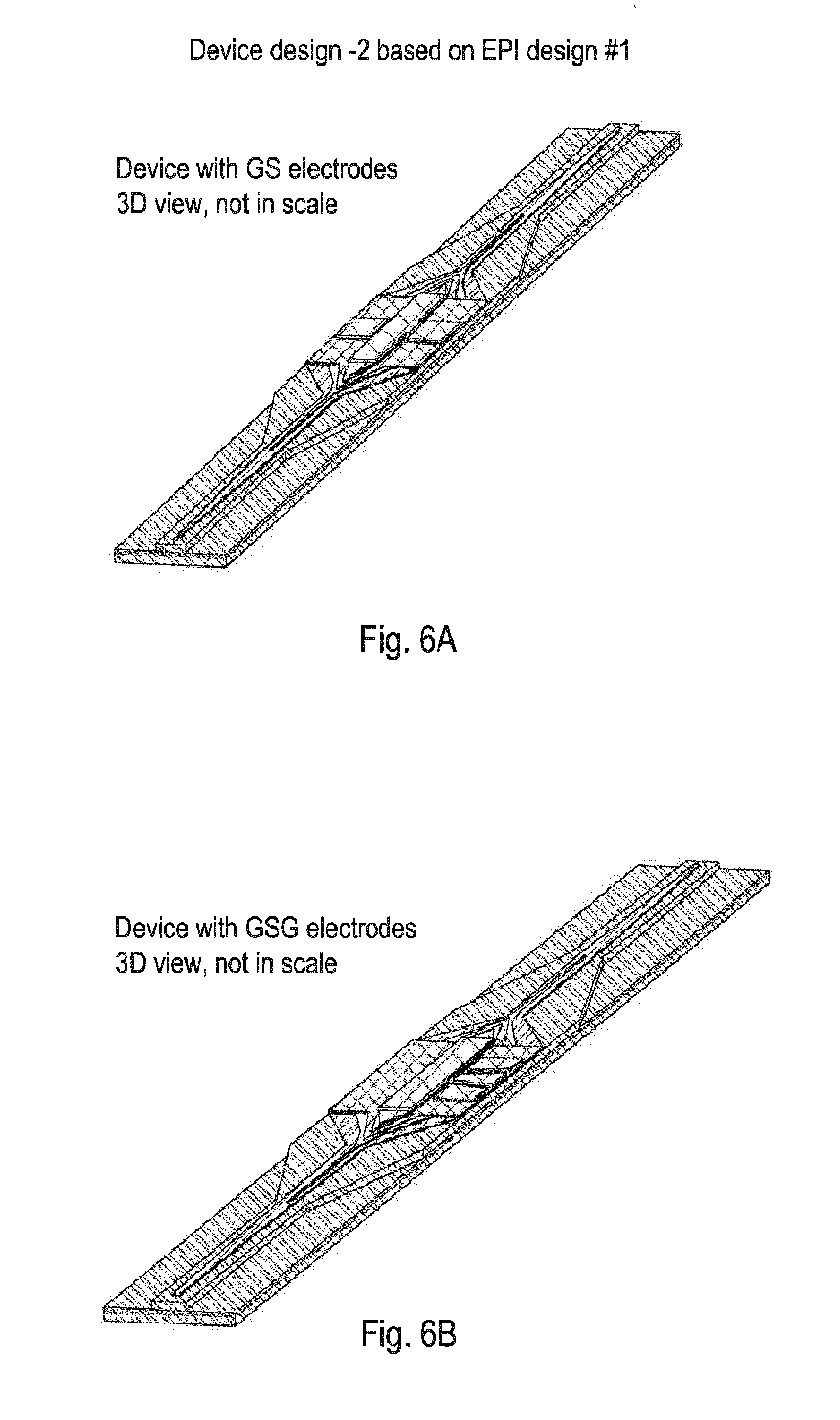
[0034] FIG. 6B is a 3D view of a device design #2 based on the SiGe epitaxial layer structure shown in FIG. 1 with GSG electrode structure;
[0035] FIG. 7A is the top view of a device design #2 based on the SiGe epitaxial layer structure shown in FIG. 1 with GS electrode structure;
[0036] FIG. 7B is the top view of a device design #2 based on the SiGe epitaxial layer structure shown in FIG. 1 with GSG electrode structure;
[0037] FIG. 8 shows the device design #2 top view with detailed device structure for each section;
[0038] FIG. 9 is the section view along the middle line KK' of the device design #2;
[0039] FIG. 10 is another SiGe epitaxial layer structure including a multiple QW structure, according to an embodiment of the present invention;
[0040] FIG. 11 shows the device design #3 top view with detailed device structure for each section based on the SiGe epitaxial layer structure shown in FIG. 10 with GS electrode structure;
[0041] FIG. 12 is the section view along the middle line KK' of the device design #3;
[0042] FIG. 13 is another SiGe epitaxial layer structure including a multiple QW structure, according to an embodiment of the present invention;
[0043] FIG. 14 shows the device design #4 top view with detailed device structure for each section based on the SiGe epitaxial layer structure shown in FIG. 13 with GS electrode structure;
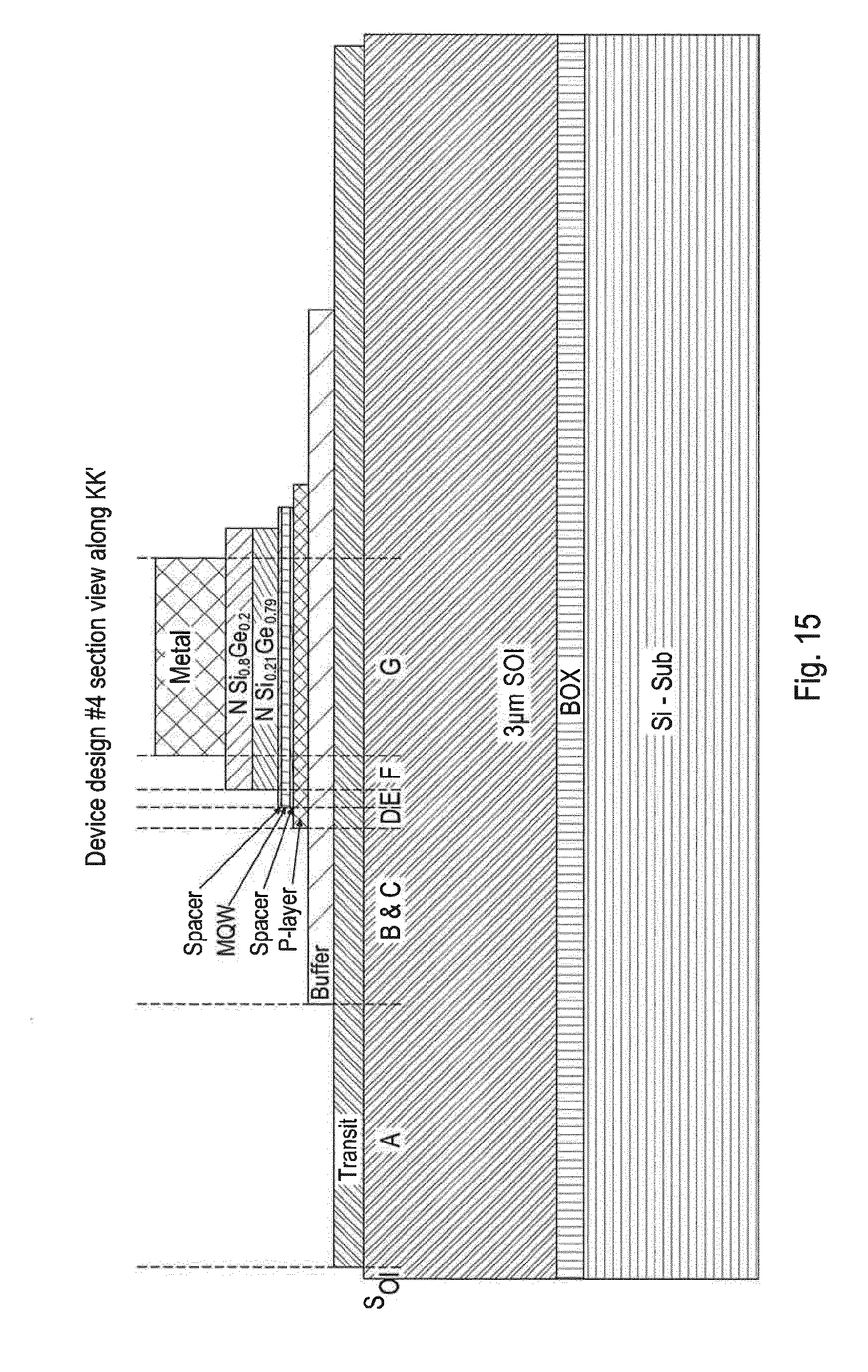
[0044] FIG. 15 is the section view along the middle line KK' of the device design #4;
[0045] FIG. 16 is the input/output 3 .mu.m SOI waveguide for use with all devices disclosed herein; and
[0046] FIG. 17 is typical optical transition from 3 .mu.m SOI waveguide to SiGe MQW waveguide simulation result at 1.3 .mu.m wavelength;
[0047] FIG. 18 is the top view of a device design #5 based on any one of the SiGe epitaxial layer structures shown in FIG. 1, FIG.10 and FIG. 13, the device of FIG.18 having a GS electrode structure;
[0048] FIG. 19 is the section view along the middle line KK' of the device design #5
[0049] FIG.20 shows a device design #1B in a top view with detailed device structure for each section;
[0050] FIG. 21 is the section view along the middle line KK' of the device design #1B
[0051] FIG. 22 is another SiGe epitaxial layer structure including a multiple QW structure, according to an embodiment of the present invention;
[0052] FIG. 23 is another SiGe epitaxial layer structure including a multiple QW structure, according to an embodiment of the present invention;
[0053] FIG. 24 shows a device design #1C in a top view with detailed device structure for each section; and
[0054] FIG. 25 is the section view along the middle line KK' of the device design #1C.
DETAILED DESCRIPTION
[0055] The detailed description set forth below in connection with the appended drawings is intended as a description of exemplary embodiments of an electroabsorption modulator provided in accordance with the present invention and is not intended to represent the only forms in which the present invention may be constructed or utilized. The description sets forth the features of the present invention in connection with the illustrated embodiments. It is to be understood, however, that the same or equivalent functions and structures may be accomplished by different embodiments that are also intended to be encompassed within the spirit and scope of the invention. As denoted elsewhere herein, like element numbers are intended to indicate like elements or features.
[0056] A first embodiment ("EPI design #1) is shown in FIGS. 1 to 9.
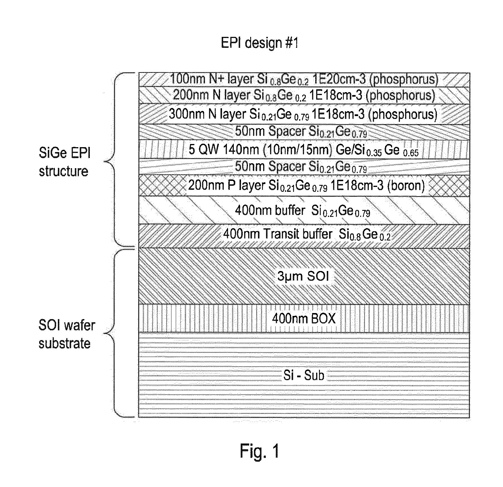
[0057] FIG. 1 shows an example of a SiGe EPI structure in accordance with the present invention in which a thin layer of transit buffer SiGe is inserted between the 3 .mu.m SOI waveguide and the SiGe buffer layer that is for the SiGe MQW.
[0058] This transit buffer SiGe layer: [0059] a) has a refractive index larger than that of Si and smaller than that of SiGe buffer layer, therefore, light can be evanescently coupled from the SOI waveguide to the transit buffer SiGe waveguide; and [0060] b) serves as an extra-buffer layer for the SiGe buffer layer of the MQW waveguide to ease the stress due to the crystal lattice mismatch between Si and SiGe MQW, which is critical for the SiGe MQW EPI quality.
[0061] The transit buffer SiGe layer shown has a germanium content of 20% (Si.sub.0.8Ge.sub.0.2). Optionally, this transit buffer SiGe layer may have a germanium content ranging from 5% (Si.sub.0.95Ge.sub.0.05) to 50% (Si.sub.0.5Ge.sub.0.5) and a thickness ranging from 400 nm to 1000 nm.
[0062] Based on the proposed SiGe EPI structure, the waveguide evanescent coupling structure brings light from the SOI waveguide (which may be a 3 .mu.m SOI waveguide) to a SiGe MQW waveguide in the following steps: [0063] a) From a SOI waveguide (which may be a 3 .mu.m SOI waveguide) to a transit buffer SiGe waveguide (which may be a 400 nm transit buffer SiGe waveguide) [0064] b) From the transit buffer SiGe waveguide (which may be a 400 nm transit buffer SiGe waveguide) to a buffer SiGe waveguide (which may be a 400 nm a buffer SiGe waveguide). The buffer SiGe layer shown has a germanium content of 79% (Si.sub.0.21Ge.sub.0.79). Optionally, this buffer SiGe layer may have a germanium content ranging from 70% (Si.sub.0.3Ge.sub.0.7) to 95% (Si.sub.0.05Ge.sub.0.95), and a thickness ranging from 400 nm to 1000 nm. [0065] c) From the buffer SiGe waveguide (which may be a 400 nm a buffer SiGe waveguide) to a SiGe MQW waveguide via a taper structure. The taper structure expends the optical mode of the buffer waveguide to the optical mode of the SiGe MQW waveguide. Wherein the taper structure and the SiGe MQW waveguide may consist of: the transit buffer SiGe, 400 nm buffer SiGe, 200 nm P-layer, 50 nm spacer, 140 nm quantum well layer (5 QW) which has 15 nm spacers between respective quantum wells which are 10 nm thick, 50 nm spacer, 300 nm N-layer, 200 nm N-doped cover layer and 100 nm heavily N-doped cover layer as shown in FIG. 1 . The P-layer, spacer layers and N-layer may have the same germanium content, (79%, Si.sub.0.21Ge.sub.0.79), as that of buffer layer. Optionally, the P-layer, spacer layers and N-layer may have a germanium content ranging from 70% (Si.sub.0.3Ge.sub.0.7) to 90% (Si.sub.0.1Ge.sub.0.9). The N-doped cover layer and heavily N-doped cover layer may have a germanium content less than that of buffer layer, P-layer, spacer layers and N-layer. The germanium content of the N-doped cover layer and heavily doped N-doped cover layer may be 20% (Si.sub.0.8Ge.sub.0.2). Optionally, the germanium content of the N-doped cover layer and heavily doped N doped cover layer may range from 5% (Si.sub.0.95Ge.sub.0.05) to 50% (Si.sub.0.5Ge.sub.0.5). The germanium content of the barrier layer in the quantum well is 65% (Si.sub.0.35Ge.sub.0.65). Optionally, the germanium content of the barrier layer in the quantum well may range from 60% (Si.sub.0.4Ge.sub.0.6) to 85% (Si.sub.0.15Ge.sub.0.85) with a general rule that the average germanium content in the Ge/Si quantum well is the same or substantially the same as the germanium content of the buffer layer. The number of quantum wells is five in this EPI structure. Optionally, the number of the quantum wells may range from 5 to 15.
[0066] The QCSE EAM consists of two coupling regions, which have two waveguide evanescent coupling structures and one taper structure, and one active region between the two coupling regions
[0067] The active region preferably has the same waveguide structure as the SiGe MQW waveguide.
[0068] Light from the Si waveguide (which may be a 3 .mu.m Si waveguide) travels through the first coupling region to reach the active region.
[0069] In the active region, light is absorbed and modulated according to the external bias voltage.
[0070] After modulation, the light goes through the second coupling region back to a/the Si waveguide (which may be a 3 .mu.m Si waveguide).
[0071] Three examples of devices which incorporate the electroabsorption modulator of the present invention are now described.
[0072] The first example (device design #1 based on EPI design #1) can be seen in the 3D views shown in FIG. 2A and FIG. 2B and also in the top views as shown in FIG. 3A (GS electrodes) and FIG. 3B (GSG electrodes). In this device design #1, the taper structure comprises 3 segments to expand the optical mode of buffer waveguide to the optical mode of SiGe MQW waveguide. An example of measurements for the entire device is shown in FIG. 4 and a section view of the device is shown in FIG. 5. The simulation results for device design #1 at 1.3 .mu.m wavelength for TE mode are below: insertion loss 4.87 dB, extinction ratio 4.16 dB and link penalty 9.97 dB.
[0073] The second example (device design #2 based on EPI design #1) can be seen in the 3D views shown in FIG. 6A and FIG. 6B and also in the top views as shown in FIG. 7A (GS electrodes) and FIG. 7B (GSG electrodes). In this device design #2, the taper structure comprises 4 segments to expand the optical mode of buffer waveguide to the optical mode of SiGe MQW waveguide. An example of measurements for the entire device of the second example (device design #2 based on EPI design #1) is shown in FIG. 8 and a section view of the device is shown in FIG. 9. The simulation results for device design #2 at 1.3 .mu.m wavelength for TE mode are below: insertion loss 4.43 dB, extinction ratio 4.16 dB and link penalty 9.53 dB.
[0074] An example (EPI design #2) and an associated device design #3 is shown in FIGS. 10-12. this embodiment differs from that of FIG. 1 (EPI design #1) in that: [0075] a) Transit buffer layer: 600 nm, Si.sub.0.9Ge.sub.0.1 [0076] b) cover N-doped layer: Si.sub.0.9Ge.sub.0.1
[0077] As with the devices described above, devices including the EPI design of the second embodiment may be fabricated with: [0078] a) GS electrodes; or [0079] b) GSG electrodes
[0080] In a third example, device design #3, the taper structure comprises 4 segments to expand the optical mode of buffer waveguide to the optical mode of SiGe MQW waveguide. The simulation results for device design #3 at 1.3 .mu.m wavelength for TE mode are below: insertion loss 4.87 dB, extinction ratio 4.16 dB and link penalty 9.97 dB.
[0081] A third embodiment (EPI design #3) of the present invention and an associated device design #4 is shown in FIGS. 13-15. This embodiment differs from that of FIG. 1 (EPI design #1) in that: [0082] a) Transit buffer layer: 800 nm. Si.sub.0.9Ge.sub.0.1 [0083] b) cover N-doped layer: Si.sub.0.9Ge.sub.0.1
[0084] As with the devices described above, devices including the EPI design of the third embodiment may be fabricated with: [0085] a) GS electrodes; or [0086] b) GSG electrodes.
[0087] In this device design #4, the taper structure comprises 4 segments to expand the optical mode of buffer waveguide to the optical mode of SiGe MQW waveguide. The simulation results for device design #4 at 1.3 .mu.m wavelength for TE mode are below: insertion loss 4.66 dB, extinction ratio 4.16 dB and link penalty 9.76 dB.
[0088] An example of in input (and/or output waveguide) for coupling to any one of the EPI regions described herein is shown in FIG. 16. In some embodiments, this may take the form of a 3 .mu.m SOI waveguide.
[0089] Typical optical transition from 3 .mu.m SOI waveguide to SiGe MQW waveguide simulation result at 1.3 .mu.m wavelength is shown in FIG. 17 for a half device structure. The device is symmetric, so the half structure simulation enabled relevant information to be achieved whilst conserving computer space.
[0090] FIG. 18 shows another example of a device design; "device design #5". This device design is could contain any one of the EPI structures of the embodiments (EPI design #1, EPI design #2 and EPI design #3) shown in FIG. 1, FIG. 10 and FIG. 13. The taper structure of device design #5 comprises 2 segments which act to expand the optical mode of buffer waveguide to the optical mode of SiGe MQW waveguide. An advantage of using such a taper structure with 2 segments is the ease of device fabrication process with fewer processing steps. FIG. 19 shows the section view of design #5 along the middle line KK'.
[0091] A fourth embodiment (EPI design #1B) of the present invention and associated device design is shown in FIG. 20-21.
[0092] An example of measurements for the entire device is shown in FIG. 20, and a section view of the device is shown in FIG. 21. This design differs from that shown in, for example, FIG. 14, in at least that the electrodes of FIG. 20 which are in contact with a surface of the active region opposite the coupler extend beyond the main body of the active region in a direction towards their respective taper regions. In this embodiment, the MQW region comprises a main section in the main body of the active region, but also includes at least one tapered portion of MQW material which extends from the main body of the active material forming active tapered portions overlaying the tapered layers underneath. As can be seen in FIG. 20, the tapered portions of the MQW material therefore extend outwards from the main body of the active region (marked "E") into at least the active mode expander region (marked "D").
[0093] A fifth embodiment (EPI design #1B (Modified)) of the present invention is shown in FIG. 22. in which a thin layer of transit buffer SiGe is inserted between the 3 .mu.m SOI waveguide and the SiGe buffer layer that is for the SiGe MQE. Broadly it is a modified version of the EPI structure corresponding with the device in FIGS. 20 and 21.
[0094] This embodiment differs from that of FIG. 1 in that:
[0095] a) the lower N layer comprises Si.sub.0.24Ge.sub.0.76 and is 100 nm thick;
[0096] b) the spacer layers comprise Si.sub.0.21Ge.sub.0.79 and are 20 nm thick;
[0097] c) the MQW region comprises 10 quantum wells, is 232 nm thick, has 12 nm spaces between quantum wells which are 10 nm thick, and comprises Ge/Si.sub.0.44Ge.sub.0.56; and
[0098] d) there is no discrete `P-layer`, instead the buffer layer is doped with P-type dopants to a concentration of 1.times.10.sup.18 cm.sup.-3 and comprises Si.sub.0.24Ge.sub.0.76.
[0099] A sixth embodiment (EPI design #1C (Modified)) of the present invention and associated device design is shown in FIG. 23-25.
[0100] An example of measurements of the entire device is shown in FIG. 24, and a section view of the device is shown in FIG. 25. The active region could contain an EPI structure as shown in FIG. 22 or FIG. 23.
[0101] FIG. 23 shows an example of a SiGe EPI structure in accordance with the present invention in which a thin layer of transit buffer SiGe is inserted between the 3 .mu.m SOI waveguide and the SiGe buffer layer that is for the SiGe MQW.
[0102] This embodiment differs from that of FIG. 1 in that:
[0103] a) the N layer adjacent to the spacer layer comprises Si.sub.0.24Ge.sub.0.76 and is 100 nm thick;
[0104] b) the spacer layers both comprise Si.sub.0.24Ge.sub.0.76;
[0105] c) the MQW region comprises 7 quantum wells, is 166 nm thick, has 12 nm spaces between respective quantum wells which are 10 nm thick, and comprises Ge/Si.sub.0.44Ge.sub.0.56; and
[0106] d) there is no discrete `P-layer` below the multiple quantum well region, instead the buffer layer is doped with P-type dopants to a concentration of 1.times.10.sup.18 cm.sup.-3 and comprises Si.sub.0.24Ge.sub.0.76.
[0107] A further difference between the device shown in FIG. 4 and those shown in FIGS. 20 and 24 is that the electrodes of FIGS. 20 and 24 which are in contact with a surface of the active region opposite the coupler extend beyond the active region in a direction towards their respective taper regions. For example, the electrodes in FIGS. 20 and 24 have a length in the direction towards the taper region which is greater than 2.5 .mu.m.
[0108] Although exemplary embodiments of an electroabsorption modulator have been specifically described and illustrated herein, many modifications and variations will be apparent to those skilled in the art. Accordingly, it is to be understood that an electroabsorption modulator constructed according to principles of this invention may be embodied other than as specifically described herein. The invention is also defined in the following claims, and equivalents thereof.
* * * * *
D00000
D00001
D00002
D00003
D00004
D00005
D00006
D00007
D00008
D00009
D00010
D00011
D00012

D00013

D00014

D00015
D00016

D00017

D00018

D00019

D00020

D00021

D00022

D00023

D00024

XML
uspto.report is an independent third-party trademark research tool that is not affiliated, endorsed, or sponsored by the United States Patent and Trademark Office (USPTO) or any other governmental organization. The information provided by uspto.report is based on publicly available data at the time of writing and is intended for informational purposes only.
While we strive to provide accurate and up-to-date information, we do not guarantee the accuracy, completeness, reliability, or suitability of the information displayed on this site. The use of this site is at your own risk. Any reliance you place on such information is therefore strictly at your own risk.
All official trademark data, including owner information, should be verified by visiting the official USPTO website at www.uspto.gov. This site is not intended to replace professional legal advice and should not be used as a substitute for consulting with a legal professional who is knowledgeable about trademark law.