Pull Rod And Alignment Key For A Fiber Optic Connector And Adapter
Takano; Kazuyoshi ; et al.
U.S. patent application number 16/240450 was filed with the patent office on 2019-08-01 for pull rod and alignment key for a fiber optic connector and adapter. The applicant listed for this patent is Senko Advanced Components, Inc. Invention is credited to Jeffery Gniadek, Kazuyoshi Takano.
| Application Number | 20190235178 16/240450 |
| Document ID | / |
| Family ID | 67392100 |
| Filed Date | 2019-08-01 |


View All Diagrams
| United States Patent Application | 20190235178 |
| Kind Code | A1 |
| Takano; Kazuyoshi ; et al. | August 1, 2019 |
PULL ROD AND ALIGNMENT KEY FOR A FIBER OPTIC CONNECTOR AND ADAPTER
Abstract
An optical connector holding one or more LC-type optical ferrules is provided. The optical connector includes an outer housing, pin keep, and two pins. One pin acts as a push/pull mechanism to release the connector from the adapter. The pin keep has two side clips with one of two side clips having an alignment key on a top surface. The alignment key engages a corresponding surface in the adapter housing to aid in polarity setting of the connector with the adapter. The adapter has a panel mounting clip that contains one or more latches that engage and retain the connector in the adapter housing. The panel clips and surfaces of the connector are constructed to reduce the overall size of the connector and adapter. The adapter has a plural of internal ribs forming one or more channels.
| Inventors: | Takano; Kazuyoshi; (Tokyo, JP) ; Gniadek; Jeffery; (Oxford, ME) | ||||||||||
| Applicant: |
|
||||||||||
|---|---|---|---|---|---|---|---|---|---|---|---|
| Family ID: | 67392100 | ||||||||||
| Appl. No.: | 16/240450 | ||||||||||
| Filed: | January 4, 2019 |
Related U.S. Patent Documents
| Application Number | Filing Date | Patent Number | ||
|---|---|---|---|---|
| 62614189 | Jan 5, 2018 | |||
| Current U.S. Class: | 1/1 |
| Current CPC Class: | G02B 6/3821 20130101; G02B 6/3882 20130101; G02B 6/3825 20130101; G02B 6/3851 20130101; G02B 6/3834 20130101; G02B 6/3893 20130101; G02B 6/3831 20130101 |
| International Class: | G02B 6/38 20060101 G02B006/38 |
Claims
1. A fiber optic connector with a pull release comprising: one or more ferrules having one or more optical fibers therein; the ferrule is contained with a housing, the housing further comprises an inner front body, the inner front body has a pair of opposing arms with a pin retainer configured to allow a pin to be moved forward and rearward; a first pin is longer than a second pin, the first pin is configured to move the second pin when the first pin is slide longitudinally; and wherein a tapered section of each pin lifts an adapter latch, thereby releasing the connector from an adapter channel.
2. A pin for lifting an adapter latch comprising: the pin comprises a longitudinal shaft; a proximal end of the pin shaft has a tapered surface; and the pin extends distally beyond a connector housing for user access to remove the connector from within an adapter channel, and wherein the tapered surface of the pin lifts an adapter latch hook to release the connector form the adapter channel.
3. An adapter comprising: an outer housing; an opening at one end or both ends of the housing; the two openings forming a longitudinal path through the connector housing allowing for two opposing fiber optic connectors to transmit a signal from a first connector to a second connector when the connectors are opposing each other; a plural of ribs along one side of inner surface of adapter housing and a corresponding rib along an opposing inner side of adapter housing, and wherein a first rib and a second rib along an inner surface form a first channel for accepting a fiber optic connector.
Description
RELATED APPLICATION
[0001] This application claims priority to U.S. provisional patent application 62/614,189 filed Jan. 5, 2018, titled "Pull Rod and Alignment Key Connector".
FIELD OF THE INVENTION
[0002] The present invention relates to optical fiber connectors and adapters, and more particularly, to push/pull mechanisms to release a connector from an adapter and a polarity changing mechanism to align the connector polarity with the adapter polarity for proper signal transmission.
BACKGROUND
[0003] The prevalence of the Internet has led to unprecedented growth in communication networks. Consumer demand for service and increased competition has caused network providers to continuously find ways to improve quality of service while reducing cost.
[0004] Certain solutions have included deployment of high-density interconnect panels. High-density interconnect panels may be designed to consolidate the increasing volume of interconnections necessary to support the fast-growing networks into a compacted form factor, thereby increasing quality of service and decreasing costs such as floor space and support overhead. However, room for improvement in the area of data centers, specifically as it relates to fiber optic connects, still exists. For example, manufacturers of connectors and adapters are always looking to reduce the size of the devices, while increasing ease of deployment, robustness, and modifiability after deployment. In particular, more optical connectors may be needed to be accommodated in the same footprint previously used for a smaller number of connectors in order to provide backward compatibility with existing data center equipment. For example, one current footprint is known as the small form-factor pluggable transceiver footprint (SFP). This footprint currently accommodates two LC-type ferrule optical connections. However, it may be desirable to accommodate four optical connections (two duplex connections of transmit/receive) within the same footprint. Another current footprint is the quad small form-factor pluggable (QSFP) transceiver footprint. This footprint currently accommodates four LC-type ferrule optical connections. However, it may be desirable to accommodate eight optical connections of LC-type ferrules (four duplex connections of transmit/receive) within the same footprint.
[0005] In communication networks, such as data centers and switching networks, numerous interconnections between mating connectors may be compacted into high-density panels. Panel and connector producers may optimize for such high densities by shrinking the connector size and/or the spacing between adjacent connectors on the panel. While both approaches may be effective to increase the panel connector density, shrinking the connector size and/or spacing may also increase the support cost and diminish the quality of service.
[0006] In a high-density panel configuration, adjacent connectors and cable assemblies may obstruct access to the individual release mechanisms. Such physical obstructions may impede the ability of an operator to minimize the stresses applied to the cables and the connectors. For example, these stresses may be applied when the user reaches into a dense group of connectors and pushes aside surrounding optical fibers and connectors to access an individual connector release mechanism with his/her thumb and forefinger. Overstressing the cables and connectors may produce latent defects, compromise the integrity and/or reliability of the terminations, and potentially cause serious disruptions to network performance.
[0007] While an operator may attempt to use a tool, such as a screwdriver, to reach into a dense group of connectors and activate a release mechanism, adjacent cables and connectors may obstruct the operator's line of sight, making it difficult to guide the tool to the release mechanism without pushing aside the adjacent cables. Moreover, even when the operator has a clear line of sight, guiding the tool to the release mechanism may be a time-consuming process. Thus, using a tool may not be effective at reducing support time and increasing the quality of service.
BRIEF DESCRIPTION OF THE DRAWINGS
[0008] FIG. 1 is a perspective view of the connector;
[0009] FIG. 2 is an exploded view of the connector of FIG. 1;
[0010] FIG. 2A is a cut-away of FIG. 1 connector with outer housing removed showing pins secured therein;
[0011] FIG. 3 is a perspective view of connector housing and pin keep assembly;
[0012] FIG. 4 is a perspective view of the pin keep assembly retracted from the connector housing;
[0013] FIG. 5 is a perspective view of an adapter with panel mounting clip installed;
[0014] FIG. 6 is an exploded view of the adapter of FIG. 5.;
[0015] FIG. 7A is a perspective views of a pin guide insert;
[0016] FIG. 7B is a perspective view of the connector body of FIG. 1;
[0017] FIG. 8A is a perspective view of a prior art adapter;
[0018] FIG. 8B is a perspective view of an adapter according to the present invention;
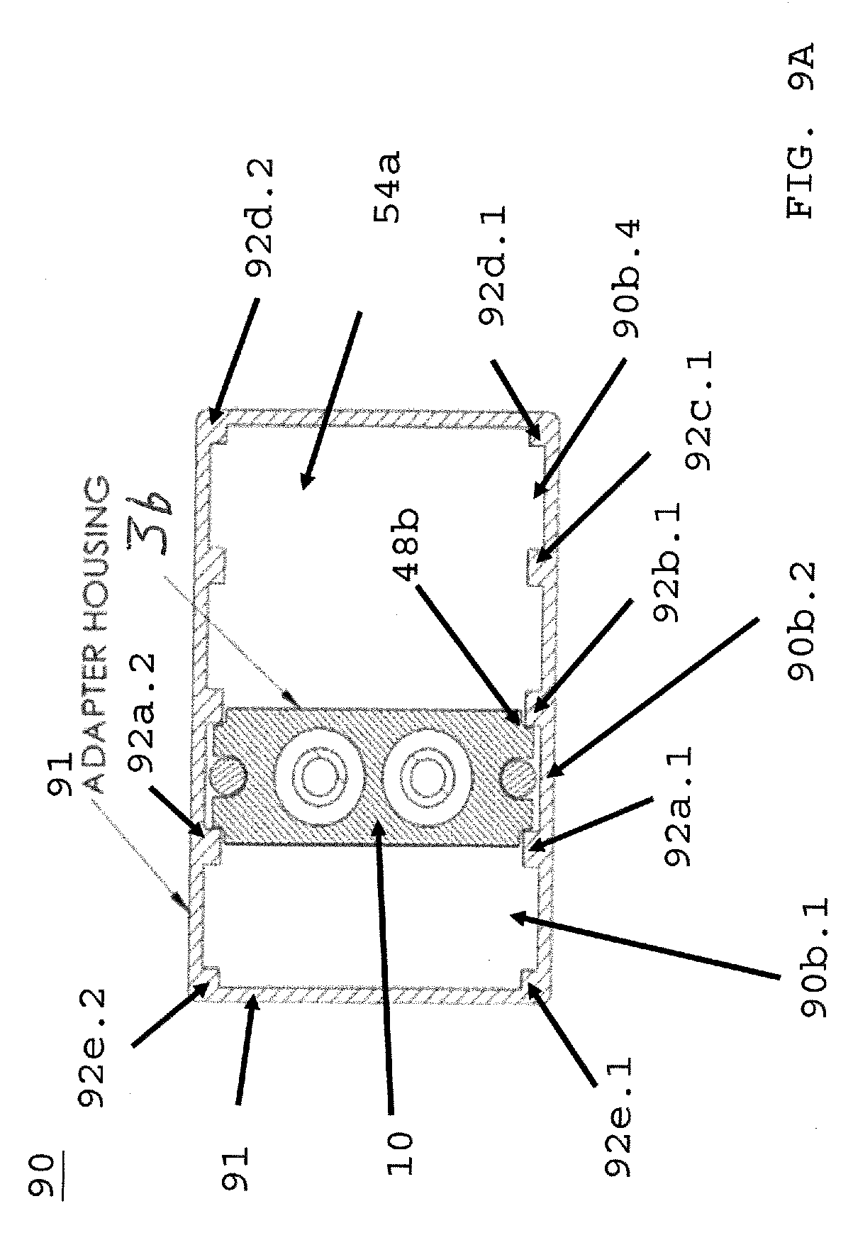
[0019] FIG. 9A is a cross section view of the adapter of FIG. 8B with the connector of FIG. 1 inserted therein; and
[0020] FIG. 9B is a perspective view of the proximal end of the connector housing of FIG. 1 illustrating notched corners.
DETAILED DESCRIPTION
[0021] A connector, as used herein, refers to a device and/or components thereof that connects a first module or cable to a second module or cable. The connector may be configured for fiber optic transmission or electrical signal transmission. The connector may be any suitable type now known or later developed, for example, embodiments of multiple-fiber push-on/pull-off (MPO) connector 10 as shown in FIG. 1. FIG. 1 depicts a connector (10) as proximal end (12) and a distal end (14). The proximal end (10) is inserted into an adapter (not shown), and the distal end (14) is in electrical communication with a signal that contains data or information. The connector opening (16) exposes two ferrules (18a, 18b) used for transmit and receive of the signal. The ferrule springs (19a, 19b) hold the ferrules as known in the prior art.
[0022] FIG. 2 shows an exploded view of the connector of FIG. 1 according to an embodiment of the present invention. Referring to FIG. 2, connector assembly (10a) shows a long pin (20) that when retracted releases the connector (10) from the adapter (not shown). An alignment key (30) (also refer to FIG. 3), on side clip (24) guides connector (10) into an adapter (not shown). Side clips (24, 26) also form an outer housing or pin keeper (32) for the long (20) and short (22) pins. In operation, the long pin is retracted and the short pin moves contemporaneously with long pin. A taper (20a) on the long pin (20) and a taper (22a) on the short pin (22) engage an adapter latch (not shown) on an adapter mounting clip (not shown), which releases the connector (10) of FIG. 1, from the adapter (not shown). The tapers, adapter and mounting clips are shown in FIG. 2. FIG. 2A depicts connector (10) without outer housing and illustrates pins (20,22) inserted into connector and secured by pin retainer bracket (70), refer to FIG. 7A.
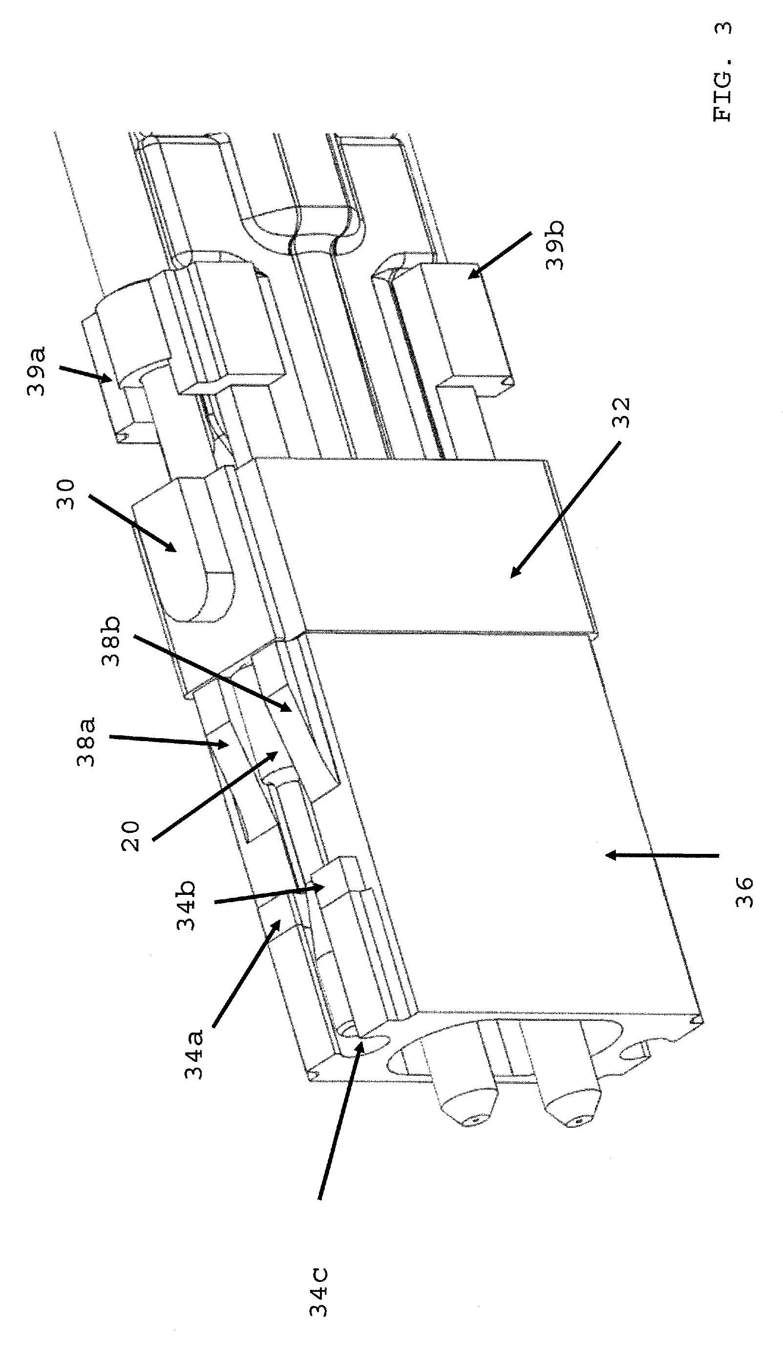
[0023] FIG. 3 shows the connector (10) housing with the pin keeper (32) formed by the side clips (24, 26). On a top surface of the pin keeper (32) is an alignment key (30) at the distal end (14) of the connector (10). Nearer the proximal end (12) is a pair of adapter hook latch surfaces (34a, 34b). The surfaces (34a, 34b) form a channel (34c) that accepts the proximal end of the long pin (20). The distal end of the surfaces (34a, 34b) further comprises a metal face or similar reinforced surface such as a hard plastic. The reinforced face is needed to protect against wear from the metal adapter hooks (not shown) that are part of the adapter mounting plate (not shown). Connector (10) has an upper pin guide (39a) and a lower pin guide (39b) in which the pins (20,22) slide from front to back, and back during operation.
[0024] Referring to FIG. 3, alignment key (30), upper housing (36) and pin keeper (32) form the connector housing (31). The alignment key (30) is molded into either side clip (24, 26). In operation, the alignment key (30) is on a top side of the connector housing (31) which indicates a first polarity, or is on a bottom side of the connector housing (31) which indicates a second polarity. The first and second polarity are different. Upon insertion of the connector (10) into the adapter, alignment key (30) engages with a cutout (not shown) that corresponds to the outer dimensions of alignment key (30). The final orientation ensures the connector (10) signal can be transmitted to the corresponding connector inserted on the opposite side of an adapter housing (50). An adapter latch (64a-64d) (refer to FIG. 6) engages adapter latching surface (38a) to secure connector (10) within a channel of a first adapter opening (50a.1) or a second adapter opening (50a.2). A channel is indicated using an alignment key cut-out (50b.1-50b.4 (refer to FIG. 5) 80b.1-80b.4; 81b.1-81b.4 (refer to FIG. 8A)) on a side of adapter housing at either opening. The connector (10) is secured via latch (66a) when the connector (10) is inserted into the adapter (50).
[0025] FIG. 4 a perspective view of connector housing (36) with pin keeper (32) housing retracted exposing springs. As the long pin (20) is retracted the pin keeper housing (36) moves distally and the tapered sections of the long (20a) and short pin (not shown) cause the adapter latch (62) to be lifted thereby releasing the connector from the adapter housing (50). The outer portion of the connector housing (36) has a metal plate (46a, 46b) insert-molded on the top side of a wall (44a, 44b) that form channels (42a, 42b) that accept pins front portion (20a, 22a (refer to FIG. 2). The metal plate increases latching strength of a connector (10) within the adapter (50). This also eliminates wear from the adapter metal latching hooks (64a-64d; 65a-65d) (refer to FIG. 6). Each wall (44a, 44b) has outer notched corners (48a, 48b) that engage internal ribs (92a, 92b, 92c, 92d, 92e) (refer to FIG. 9A) positioned on inside wall of adapter (50). This improves side load restraint for individual connectors (10) being inserted into the adapter (50) channel (50b.1-50b.4). The internal ribs (92a, 92b) (refer to FIG. 9A) side by side form a channel (90b.1-90b.4).
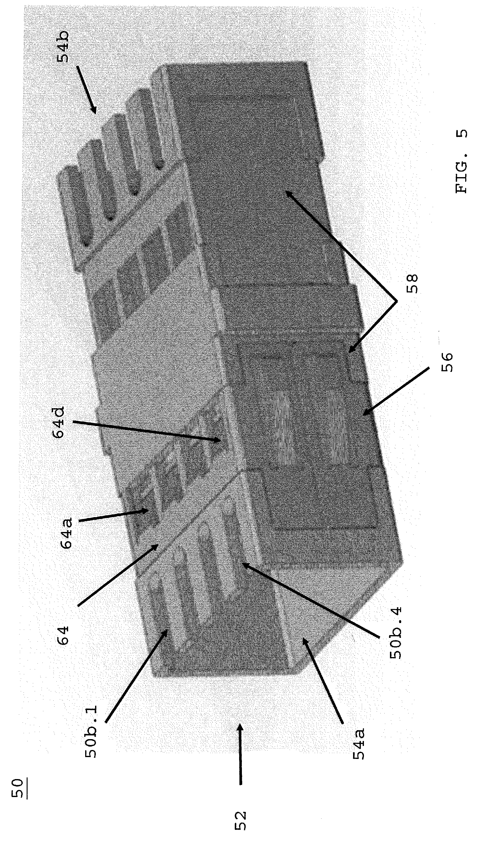
[0026] FIG. 5 is a perspective view of an adapter (50). The adapter (50) has a panel mounting clip (56) attached to the adapter outer housing at the proximal end of the adapter (52). The distal end or opposite end has a recess (58) for accepting a clip (56). A connector is inserted into the adapter through the receptacle (54), in this case first opening (54a) or second opening (54b) can accept a quad connector (10) or up to four connectors (10). Connector (10) upon full insertion engages an adapter latch (64) hooks (64a-64b) respectively for each inserted connector (10). Alignment key slots (50b.1-50b.4) indicate channels within opening (54a) or opposing opening (54b).
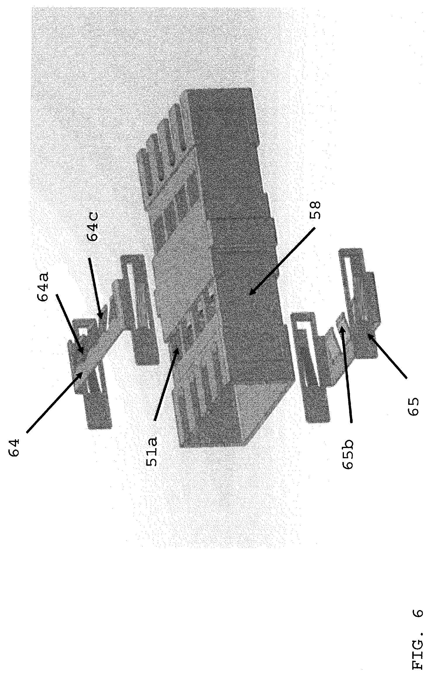
[0027] FIG. 6 is an exploded view of an adapter housing (50) with the panel clips (64, 65). The adapter latch hooks (64a-64b) are inserted into a corresponding opening (51a-51d) when panel clip (64, 65) is inserted into recess 58. Upon insertion of connector (10), latch (64a) engages the metal plate (46a), and rests on the top face of its corresponding latch adapter surface (38a). The use of the metal latches and surfaces reduces the overall size of the adapter and connector because less plastic material is needed to reach the required stress and other related performance standards.
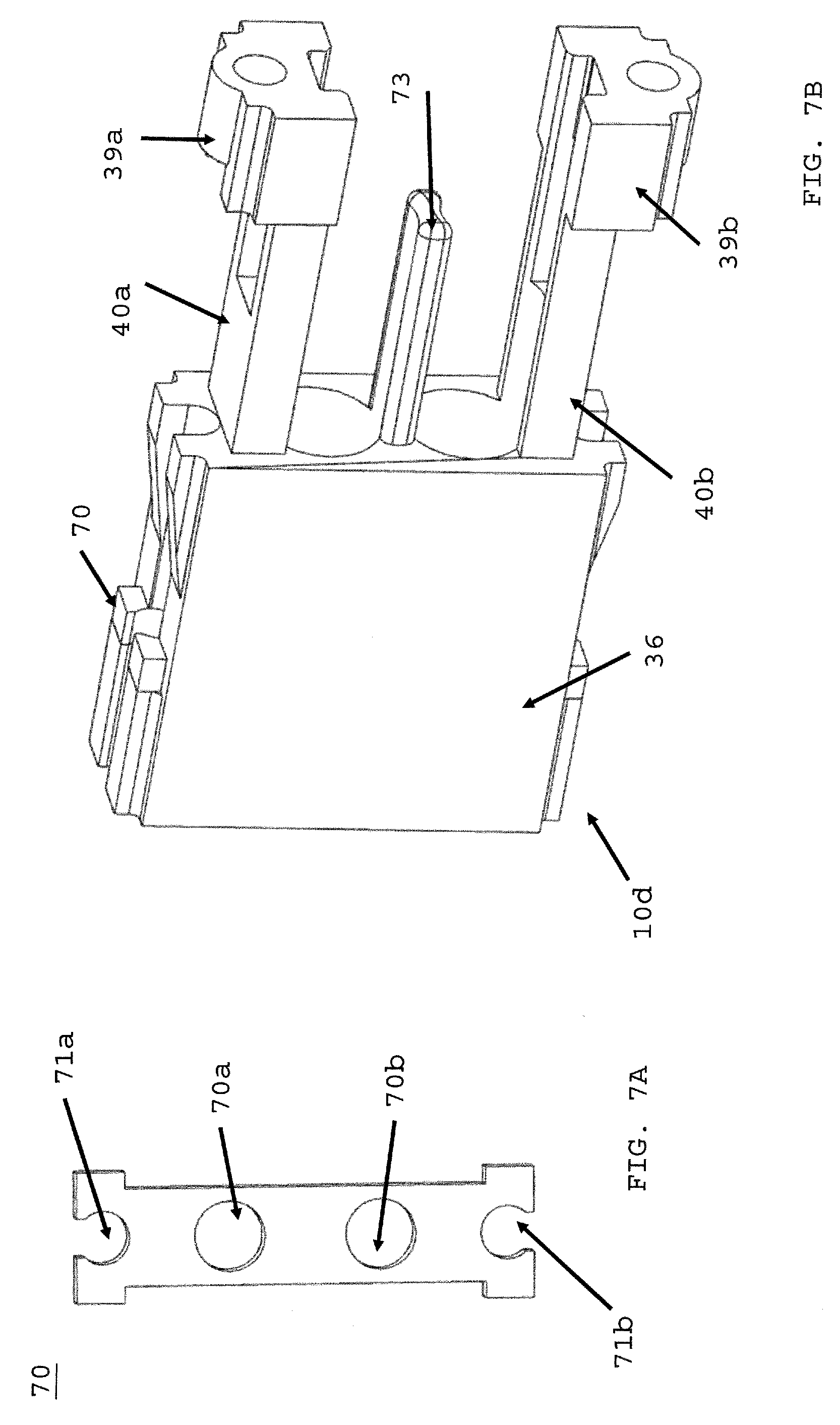
[0028] FIG. 7A is a perspective view of a mold metal insert (70) that is configured to be placed at proximal end of connector housing (10d) (refer to FIG. 7B). The insert may be made of plastic. The insert (70) has a top u-shaped cut-out (71a) and bottom u-shaped cut-out (71b) configured to accept a proximal end of pins (20a, 22a). Inert (70) further comprises two openings (70a, 70b) to accept ferrules (18a, 18b). FIG. 7B is a perspective view of the connector front (10d). Metal insert (70) is optional, and will eliminate wear from contact with the adapter latches (64, 65) on top of connector housing (36). Front body (10d) has a pair of opposing arms (40a, 40b) at a distal end. The arms further comprise a pin retainer and guide (39a, 39b) with an opening to accept either pin (20, 22). Arms (40a, 40b) cooperate with middle wall (73) to guide ferrule (18a, 18b) insertion into front body (10d) from a distal end of said body.
[0029] FIG. 8A is an adapter housing (80), with openings (51a-51d) configured to receive latch hooks (64a-64d) formed as part of a clip (64). Latch hooks (64a-64d) described above secure connector (10). Adapter (80) does not have internal ribs (see FIG. 8B, 9A) within adapter and the ribs form a channel as described below. Adapter has slots (80a.1-80d.1) for alignment key (30) on connector (10) where the key (30) indicates polarity. FIG. 8B is an adapter housing (82) with a top supporting surface (84) added to secure and stabilize the panel mounting clips (64, 65).
[0030] FIG. 9A is perspective view of the connector (10) and its housing (36) illustrating notched corner (48b) configured to engage internal rib 92b.1. A rib (92a.1-92e.1; 92a.2-92e.2) is to align and support connector (10) upon insertion into a channel (90b.1, 90b.2) formed by a side-by-side rib pair (92a.1, 92b.1 and 92a.2, 92b.2) on an inside wall surface of receptacle or adapter opening (54a). Ribs are located along one inner side of adapter housing (91) and corresponding rib along an opposing wall of housing (91). FIG. 9B is a cross section of the adapter housing (50) with a connector (10) inserted. Referring to FIG. 9A and FIG. 9B, notched corners (48a, 48b or 49a, 49b) (refer to FIG. 9B), engage and accept their respective rib (92a.1, 92b.1; 92a.2, 92b.2) to reduce side loading and aid in location of the connector within the adapter housing (91). The rib pairs (92e.1,92a.1; 92e.2, 92a.2) form a channel (90b.1) within opening (54a) of adapter (90). The rib pairs (92a.1, 92b.1; 92a.2, 92b.2) form channel (90b.2). Other rib pairs form remaining channels (90b.3, 90b.4). The ribs reduce the overall size of the adapter thereby reducing the overall adapter foot print. This reduces space within a data center.
[0031] The embodiments were chosen and described in order to best explain the principles of the invention and its practical application, thereby enabling others skilled in the art to understand the invention for various embodiments and with various modifications that are suited to the particular use contemplated.
* * * * *
D00000
D00001
D00002
D00003
D00004
D00005
D00006
D00007
D00008
D00009
D00010
D00011
D00012

XML
uspto.report is an independent third-party trademark research tool that is not affiliated, endorsed, or sponsored by the United States Patent and Trademark Office (USPTO) or any other governmental organization. The information provided by uspto.report is based on publicly available data at the time of writing and is intended for informational purposes only.
While we strive to provide accurate and up-to-date information, we do not guarantee the accuracy, completeness, reliability, or suitability of the information displayed on this site. The use of this site is at your own risk. Any reliance you place on such information is therefore strictly at your own risk.
All official trademark data, including owner information, should be verified by visiting the official USPTO website at www.uspto.gov. This site is not intended to replace professional legal advice and should not be used as a substitute for consulting with a legal professional who is knowledgeable about trademark law.