High Power Charge Pump With Inductive Elements
ILLIANO; Enzo
U.S. patent application number 16/331054 was filed with the patent office on 2019-07-25 for high power charge pump with inductive elements. The applicant listed for this patent is Brusa Elektronik AG. Invention is credited to Enzo ILLIANO.
| Application Number | 20190229616 16/331054 |
| Document ID | / |
| Family ID | 59859041 |
| Filed Date | 2019-07-25 |


| United States Patent Application | 20190229616 |
| Kind Code | A1 |
| ILLIANO; Enzo | July 25, 2019 |
HIGH POWER CHARGE PUMP WITH INDUCTIVE ELEMENTS
Abstract
A high power unidirectional or bidirectional charge pump with inductive elements for high power DC-DC converter applications. Inductive elements resonating with storage capacitors allow zero current switching processes. Storage elements in the form of capacitors instead of conventional inductors allow a cheap and lightweight construction. The output voltage cannot be actively regulated and corresponds to a fraction of the input voltage. However, several voltage ratios can be easily obtained between output and input, such as 0.25, 0.33, 0.5, 0.75, 1.25 1.33, 1.5, 2, 3, and 4.
| Inventors: | ILLIANO; Enzo; (Lugano, CH) | ||||||||||
| Applicant: |
|
||||||||||
|---|---|---|---|---|---|---|---|---|---|---|---|
| Family ID: | 59859041 | ||||||||||
| Appl. No.: | 16/331054 | ||||||||||
| Filed: | August 30, 2017 | ||||||||||
| PCT Filed: | August 30, 2017 | ||||||||||
| PCT NO: | PCT/EP2017/071770 | ||||||||||
| 371 Date: | March 6, 2019 |
| Current U.S. Class: | 1/1 |
| Current CPC Class: | H02M 3/335 20130101; H02M 2001/0093 20130101; Y02B 70/1491 20130101; H02M 3/073 20130101; H02M 3/158 20130101; H02M 3/07 20130101; H02M 1/083 20130101; Y02B 70/10 20130101; H02M 2001/0058 20130101 |
| International Class: | H02M 3/07 20060101 H02M003/07; H02M 1/08 20060101 H02M001/08 |
Foreign Application Data
| Date | Code | Application Number |
|---|---|---|
| Sep 7, 2016 | DE | 10 2016 217 040.6 |
Claims
1. A DC-DC converter, comprising an input DC-link, an output DC-link, the output DC-link connected to the input DC-link by a circuit arrangement comprising at least a storage capacitor and a DC-link capacitor and at least one switching arrangement, with the controllable switching arrangement adapted to connect at least one of the capacitors and/or the input DC-link to the output DC-link, wherein an inductive element is serially connected immediately in front of the storage capacitor and both the storage capacitor and the inductive element adapted to form a resonant circuit and in that the circuit arrangement comprises a further DC-link capacitor serially connected to the DC-link capacitor, and permanently connected with the input DC-link and with the at least one switching arrangement adapted to alternatively connect the further DC-link capacitor or the input-DC-link to the storage capacitor, with the switching frequency of the at least one switching arrangement and the resonance frequency of the resonant circuit being essentially equal.
2. The converter according to claim 1, wherein one DC-link capacitor is directly connected to the input DC-link, which is also connectable to the storage capacitor via the inductive element by the at least one switching arrangement.
3. The converter according to claim 2, wherein a further DC-link capacitor is connected via a diode to either the input DC-link or after activating the at least one switching arrangement to the inductive element and the storage capacitor.
4. The converter according to claim 2, wherein one DC-link capacitor is directly connected to the input DC-link, which is also connectable to the storage capacitor via the inductive element by the at least one switching arrangement.
5. The converter according to claim 4, wherein a further DC-link capacitor is connected permanently to the output DC-link or after activating the at least one switching arrangement via a diode to the storage capacitor and the inductive element.
6. The converter according to claim 1, wherein the DC-link capacitor is directly connected to the output DC-link, which is also connectable to the storage capacitor via the inductive element by the at least one switching arrangement.
7. The converter according to claim 6, wherein a further DC-link capacitor is connected to the input DC-link or after activating the at least one switching arrangement to the inductive element and the storage capacitor.
8. The converter according to claim 1, wherein first and second diodes are connected parallel to first and second switches of the at least one switching arrangement, with a first diode parallel to a second switch being connected in reverse direction seen from the storage capacitor and a second diode parallel to a first switch being connected in open direction seen from the storage capacitor.
9. The converter according to claim 8, wherein third and fourth switches are connected parallel to third and fourth diodes, with a third switch parallel to a fourth diode connecting a first DC-link and a fourth switch parallel to a third diode connecting the inductive element to the DC-link capacitor and to the other DC-link.
10. The converter according to claim 8, wherein parallel to each of the DC-link capacitors a large resistor is connected, with large resistors being identical.
11. The converter according to claim 8, wherein a further at least one first resistor is connected between the storage capacitor and a closest large resistor and/or a further at least one second resistor is connected between the inductive element and the DC-link parallel to the DC-link capacitors.
12. The converter according to claim 9, wherein parallel to one or more switches of the first and second, and third and fourth switches highly resistive switches are connected and the converter is adapted to operate with these highly resistive switches during first switching events and changing to other switches of the first and second, and third and fourth switches thereafter.
13. The converter according to claim 1, wherein a further converter stage is connected between one capacitor of DC-link capacitors of a first converter stage, a storage capacitor of the further converter stage is connected to a DC-link capacitor of the further converter stage and the output DC-link, the latter being connectable to the input DC-link and one of the DC-link capacitor or the further DC-link capacitor as well as the storage capacitor of the further converter stage via an inductive element of the further converter stage by a first switch and/or a second switch.
14. The converter according to claim 1, wherein a further storage capacitor and a further inductive element are connected in parallel to the storage capacitor and the inductive element and capable of being activated by switches and connectable with one of the DC-link capacitor or the further DC-link capacitor being connected to the output DC-link.
15. The converter according to claim 7, wherein a further storage capacitor and a further inductive element are connected serially to the storage capacitor and inductive element via a switch and capable of being activated by a further switch and connectable with one of the DC-link capacitor or the further DC-link capacitor.
Description
CROSS-REFERENCE TO RELATED APPLICATIONS
[0001] The present application is the U.S. National Phase of PCT/EP2017/071770, filed on Aug. 30, 2017, which claims priority to German Patent Application No. 10 2016 217 040.6, filed on Sep. 7, 2016, the entire contents of which are incorporated herein by reference.
BACKGROUND
Field
[0002] The invention relates to DC-DC converters. More specifically, the invention is directed to a charge pump for high power applications, in particular, including inductive elements combined with capacitors which allow zero current switching processes and consequently a minimization of the losses.
Related Art
[0003] Efficient and lightweight DC to DC voltage conversion is required in a widespread range of applications which involve the most disparate power levels from small supplies with output powers in the mW order to large MW plants.
[0004] To obtain an efficient DC to DC conversion there are several possible topologies. However, the basic principle behind DC-DC conversion is always the same. Any topology presents an input DC link, an output DC link, and one (or more) storage element. In a first step, some energy is transferred from the input DC Link to the storage element. In a second step, energy is transferred from the storage element to the output DC link. The sequence is then repeated.
[0005] The quasi-totality of high power converters employs inductive elements as storage elements. In very low power applications it is also common to employ capacitors as storage elements, often with circuits known as charge pumps.
[0006] For high power applications, charge pumps (e.g., capacitors as storage elements) are practically never used.
[0007] Charge pumps allow extremely poor control possibilities concerning the current flow and/or the output voltage. However, the utilization of capacitors as storage elements involves significant benefits in terms of costs, weight, and manufacturing process.
[0008] A specific type of DC to DC power converter and a method of conversion is disclosed in U.S. Pat. No. 6,429,632 B1, provided using high-frequency switched capacitors where the switches are implemented by CMOS transistors or diodes on an integrated-circuit chip and using inductors to limit charging current. High efficiency is achieved using inductors to reduce energy losses in circuit capacitors by high frequency switching when inductor current is zero and capacitor voltage is maximized. The high-frequency (100 MHz or greater) operation of the converter circuit permits the use of inductors with a low inductance value on the order of 100 nH (100.times.10-9 Henrys) capable of fabrication directly on an integrated-circuit (IC) chip. The use of CMOS integrated components allows the entire converter to be formed on a single IC chip, saving significant space within the portable system. Output voltage and current is high enough to permit EEPROM programming. In addition, fluctuations in the output voltage (ripple voltage) are substantially eliminated when several of the converter circuits are used in parallel. While this type of converter is adapted for the use inside integrated circuits and operating with high currents, it is not suitable for high voltages and high power applications as for instance in hybrid or electric vehicles.
SUMMARY OF THE INVENTION
[0009] The object of the present invention is a charge pump topology suited for high power applications which does not require an accurate output voltage control.
[0010] This object is achieved by the features of independent claim 1. Further embodiments and advantageous variants of the inventive concept are given in the dependent claims, the following specification, and the accompanying drawings.
[0011] Compared to classical and widespread charge pump topologies (designed for low power applications) the design proposed herein includes inductive elements which allow a zero current switch and a resonant operation of the converter, with the special resonant waveform generated with only one coil and one capacitor. In addition, the necessary winding goods can be reduced considerably, thereby making the new converter design more cost-effective and more lightweight.
[0012] The working frequency is typically below 500 kHz, preferably spans the range from about 20 kHz to about 200 kHz. The rated input voltage is typically in the range of about 400 V and can be boosted up to 800 V, allowing for instance to charge 800 V batteries at 400 V stations or allowing the supply of 400 V systems by such 800 V batteries. Typical power values are between 20 kW up to 200 kW, but can even be lower or higher.
BRIEF DESCRIPTION OF THE DRAWINGS
[0013] The list of reference numerals is part of the disclosure. The drawing figures are described in correlation and jointly. Same reference numerals are used for the same parts. Reference numerals with different indices are used for functionally identical or similar parts.
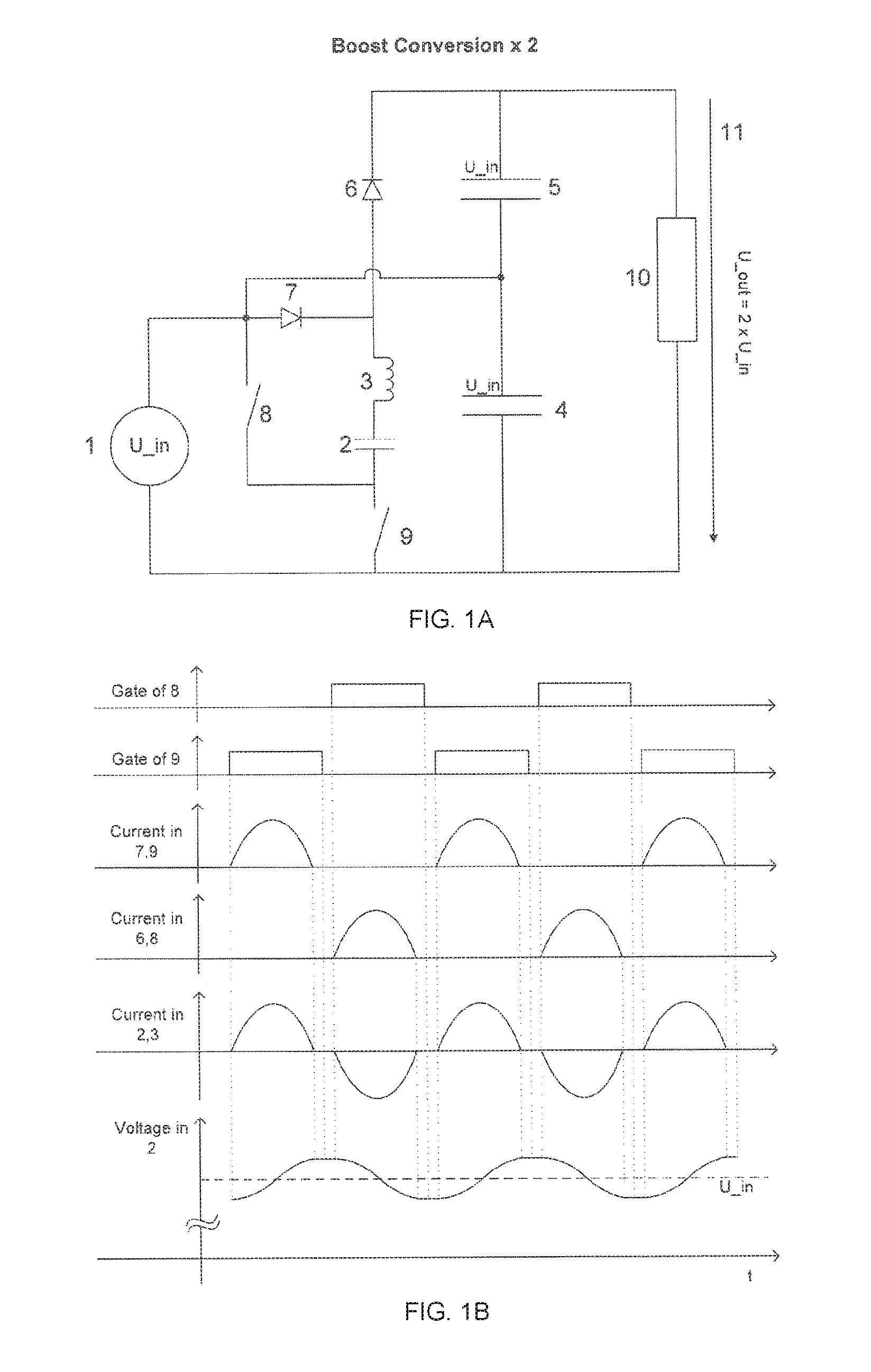
[0014] FIG. 1A shows a charge pump circuit which doubles the input voltage, and FIG. 1B shows corresponding qualitative waveforms in the main components of FIG. 1A.
[0015] FIG. 2A shows a charge pump circuit which halves the input voltage, and FIG. 2B shows corresponding qualitative waveforms in the main components of FIG. 2B.
[0016] FIG. 3 shows an embodiment of a charge pump circuit, which allows a bidirectional energy flow.
[0017] FIG. 4 shows a charge pump circuit with pre-charge elements, which allow a significant reduction of inrush currents when the device is turned on.
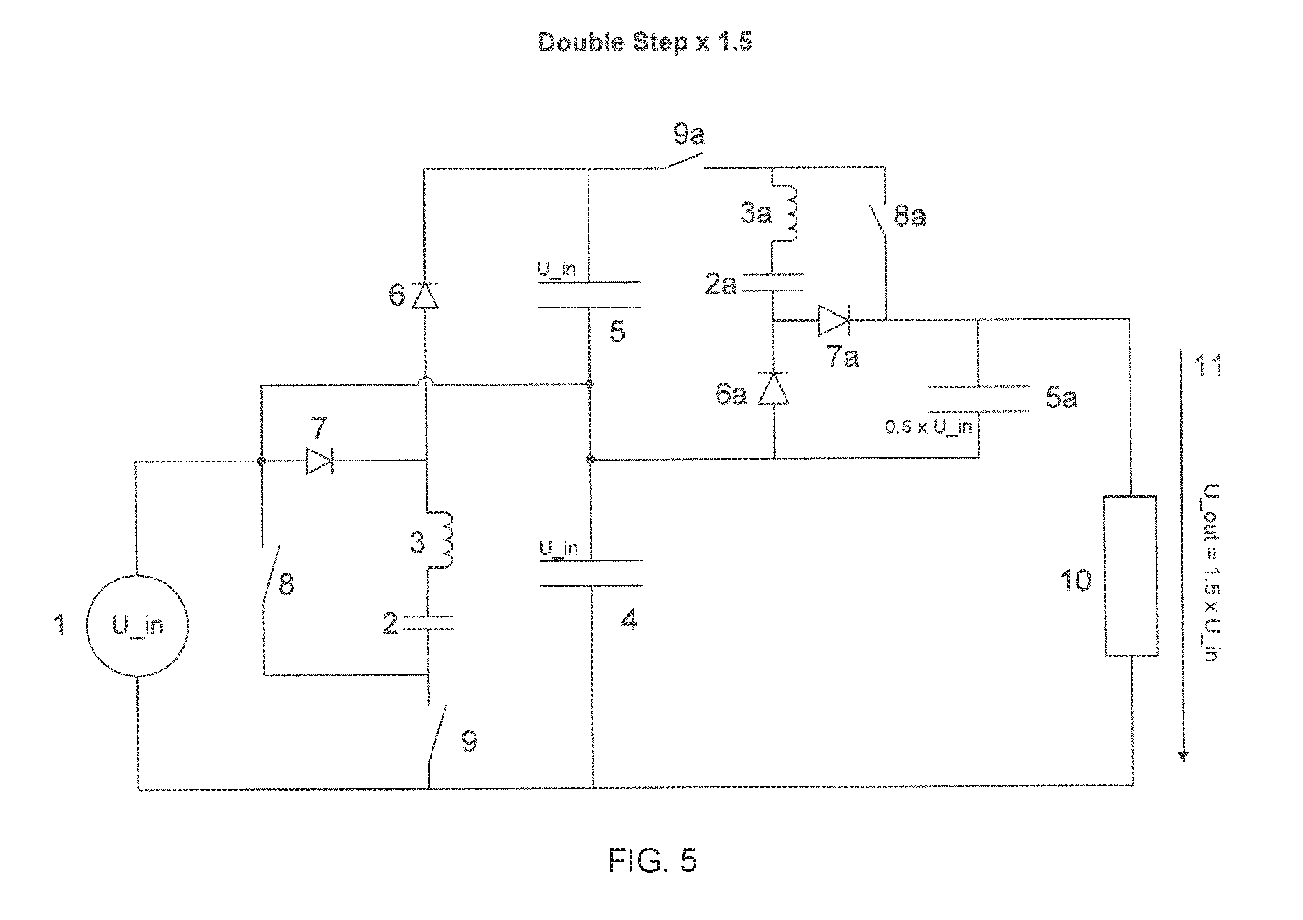
[0018] FIG. 5 shows a cascaded embodiment which generates a voltage multiplication by a factor of 1.5 using a two stage concept.
[0019] FIG. 6A shows a single step embodiment which generates a voltage multiplication by a factor of 1.5, and FIG. 6B shows the corresponding qualitative waveforms in the main components of FIG. 6A.
[0020] FIG. 7A shows a single step embodiment which generates a voltage multiplication by a factor of 1.5, and FIG. 7B shows the corresponding qualitative waveforms in the main components of FIG. 7A.
[0021] FIG. 8A shows a charge pump circuit operating at a reduced frequency to minimize switching and gate drive losses at low load, and FIG. 8B shows the corresponding qualitative waveforms in the main components of FIG. 8A.
DETAILED DESCRIPTION
[0022] FIG. 1A shows a charge pump circuit which doubles the input voltage, and FIG. 1B shows corresponding qualitative waveforms in the main components of FIG. 1A. By turning on the charging switch 9, the storage capacitor 2 is charged through the inductive element 3. In steady state condition, the process starts when the voltage on the capacitor 2 is slightly slower compared to the input DC-link voltage 1. Due to an initial voltage difference between the input DC-link 1 and the storage capacitor 2, an oscillation process with the inductive element 3 takes place. A sinusoidal current flows through the charging switch 9 and the charging diode 7. After half of the oscillation period, the diode 7 avoids a current flow in the opposite direction and the oscillation is consequently stopped. The voltage on the storage capacitor 2 remains therefore slightly higher than the voltage of the input DC-link 1. At that moment, after a short "dead time," the discharging switch 8 is turned on. Due to a voltage difference between the storage capacitor 2 and the upper DC-Link capacitor 5, which is constantly charged at the voltage U_in, an oscillation between the storage capacitor 2 and the inductive element 3 takes places. The current flow succeeds through the discharging switch 8 and the discharging diode 6. After half of the oscillation period, the diode 6 avoids a current flow in the opposite direction and the oscillation is therefore stopped.
[0023] Again, after a short "dead time" the charging switch 9 is turned on and the whole process is repeated. Each of the described switching processes can be considered as zero current transitions, and therefore the switching losses of the described system are very low. The switches are all activated and deactivated, respectively, for about 50% of the duty cycle.
[0024] For a correct operation, it is important that the resonance frequency between the components 3 and 2 is equal to or larger than the switching frequency. Nevertheless, to minimize the dead time, and thus reduce the peak current in the components, the switching frequency should possibly equal the resonance frequency.
[0025] In addition, to avoid oscillations on the output voltage, the DC-link capacitors 4 and 5 must be significantly larger than the storage capacitor 2.
[0026] The whole process described above can be summarized as follows: In a first step, energy is transferred from the bottom DC link capacitor 4 (which is connected to the input DC-Link) to the storage capacitor 2. In a second step, energy is transmitted to the top DC-link capacitor 5.
[0027] An embodiment which allows to halve the input voltage is shown in FIG. 2A, and corresponding qualitative waveforms in the main components are shown in FIG. 2B. The basic principle is very similar to the one described above. The turning on of the charging switch 9 triggers a half period oscillation which transfers energy from the top DC-Link capacitor to the storage capacitor. The activation of the discharge switch 8 triggers a half period oscillation which transfers energy to the bottom DC-link capacitor.
[0028] The combination of the two principles described above results in a bidirectional embodiment which is shown in FIG. 3. If the left side is used as input DC-Link, the charge pump works as a voltage doubler. In this case, the active semiconductor components are 8, 9, 7, and 6. Instead, if the right side of the figure is used as input DC link, the charge pump works as a voltage divider. In this case, the active components are 12, 13, 14, and 15. The diode-switch combinations 12-9, 13-8, 14-7, and 15-6 must not necessarily be separate components. Especially if MOSFETs are used, it is convenient to employ the body diodes of the semiconductor. The utilization of body diodes has an additional advantage for bidirectional embodiments.
[0029] With a bidirectional configuration it is also possible to implement the so called active rectification, e.g., activate the switch parallel to the conducting diode to reduce losses. However, it is very important that the switch is turned off before the end of the half period oscillation. If the switch is not deactivated, the diode cannot stop the oscillation after a half of the period and the operation of the circuit is significantly degraded.
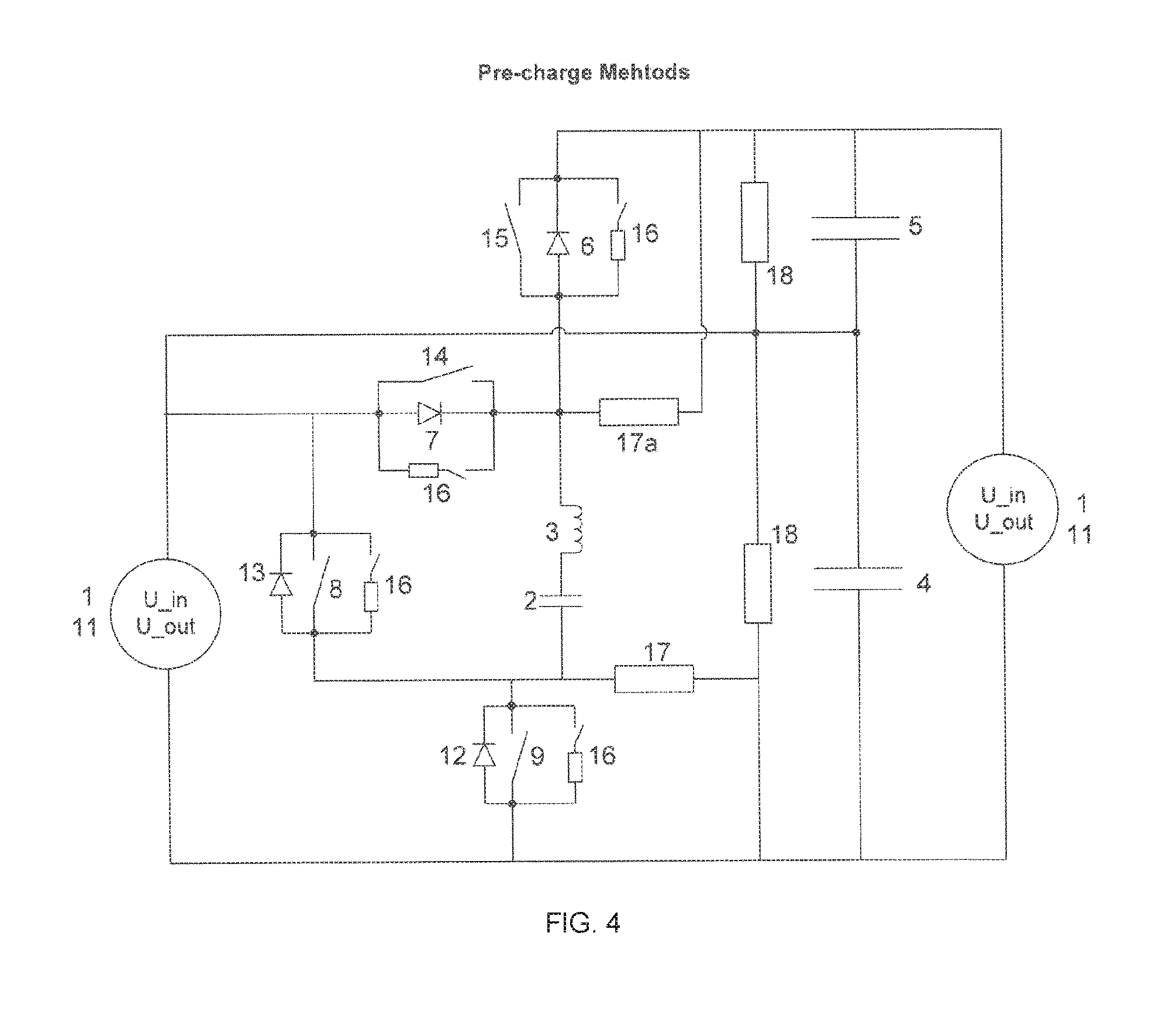
[0030] FIG. 4 proposes a solution to avoid high inrush currents while the charge pump is turned on. First of all, it is important to guarantee that the two DC link capacitors 4 and 5 are charged at the same voltage. This can be guaranteed with two identical large resistors 18. Before any switching event, it is also crucial to guarantee a pre-charge in the storage capacitor. This can be guaranteed with a resistor in positions 17 and/or 17a. If a pre-charge resistor is placed in position 17, the capacitor is charged through the diode 7 by the bottom DC-Link capacitance 4. If a pre-charge resistor is placed in position 17a, the capacitor is charged through the diode 13 by the top DC-Link capacitor 5.
[0031] Alternatively to charging resistors, it is also possible to place highly resistive switches 16 parallel to one or more of the main switches. In this way, during the first switching events only the highly resistive paths are activated, thus avoiding high currents to charge the capacitors 2, 4, and 5. Once the capacitors are charged, the system can operate normally and the main switches 8, 9, 14, and 15 can be activated.
[0032] Another option to avoid inrush currents is to operate one or more of the main switches 8, 9, 14, and 15 with very short on pulses until the capacitances of the system 4, 5, and 2 are charged.
[0033] With a bidirectional topology, as for example the one shown in FIG. 3, to balance the voltage between the DC-link capacitors, it is also possible to alternatively work in buck (voltage divider) and boost (voltage doubler) modus. In the case of a voltage divider, some charge is transferred from the top DC-link capacitor 5 to the bottom DC-link capacitor 4. Instead, in the case of a voltage doubler, some charge is transferred from the bottom DC-link capacitor 4 to the top DC-link capacitor 5. Therefore, if the top capacitor 5 voltage is too high, a buck modus operation is useful to equalize the voltage between the two DC-link capacitances. Respectively, if the bottom capacitor 4 voltage is too high, a boost modus operation is useful to equalize the voltage between the two DC-link capacitances.
[0034] A two step "cascading" charge pump embodiment is disclosed in FIG. 5. The voltage of the top DC-link capacitor 5 is halved, thus charging the output capacitor 5a with a half of the input Voltage U_in. In a completely analogous way, using two steps, it is possible to obtain following U_out/U_in ratios: 0.25, 0.75, and 1.5.
[0035] A fractional voltage ratio can also be obtained with a single step. An embodiment which boosts the voltage by a factor 1.5 is shown in FIG. 6A, and corresponding qualitative waveforms in the main components are shown in FIG. 6B. The charging process succeeds with two in series connected storage capacitances 2 and 2b, through the activation of the switches 9 and 19. The average voltage on the single storage capacitance is therefore only 0.5.times.U_in. With the activation of switches 8 and 8b, the discharge process succeeds with parallel connected storage capacitors 2 and 2b. For this reason, the upper DC-link capacitor 5 is charged with 0.5.times.U_in and consequently the output voltage 11 is 1.5.times.U_in.
[0036] The serially connected circuit 20, which is in FIG. 6A is formed by two LC oscillating circuits 2, 2b, 3, and 3b, can be also composed by more than two of these elements in series. In this way, it is possible to obtain lower voltage ratios of 1.33 (if three elements are employed), 1.25 (4 elements), 1.2 (5 elements) and so on.
[0037] It is important to notice that the embodiment of FIG. 6A can also work as a voltage doubler (if the switch 19 is constantly on and the switch 8 is constantly oft), de facto allowing a charge pump with selectable voltage ratio (in this specific case 2 or 1.5). Depending on the activated switches, one and the same circuit allows for a plurality of different voltage ratios.
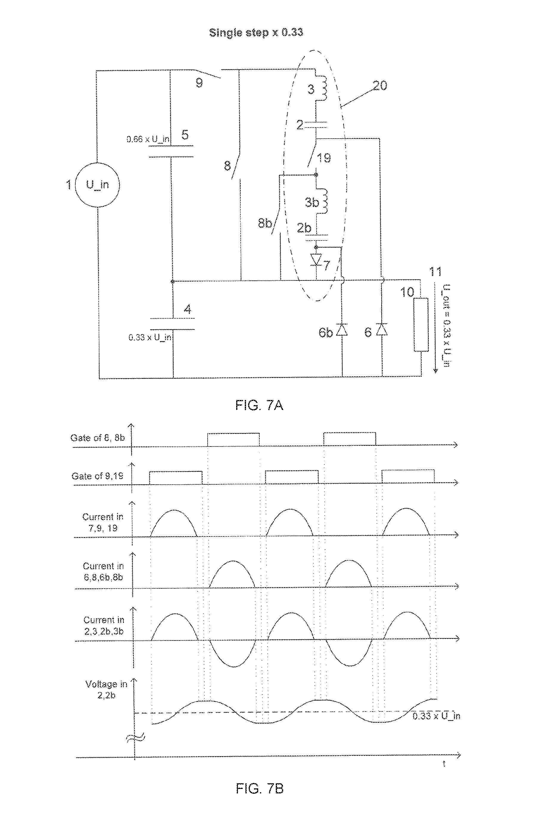
[0038] Another fractional voltage ratio can be obtained with the embodiment shown in FIG. 7A, with corresponding qualitative waveforms of the main components shown in FIG. 7B, which multiplies the voltage by a factor of 0.33. Also in this case, the charging process succeeds with two in-series connected storage capacitances (2 and 2b), through the activation of the switches 9 and 19. The average voltage on the single storage capacitance is therefore only 0.33.times.U_in. With the activation of switches 8 and 8b, the discharge process succeeds with parallel connected storage capacitors 2 and 2b. For this reason, the bottom DC-link capacitor 5 is charged with 0.33.times.U_in.
[0039] The serially connected circuit 20 which is in FIG. 6A composed of two LC oscillating circuits 2, 2b, 3, 3b can also be composed of more than two of these elements in series. In this way, it is possible to obtain lower voltage ratios of 0.25 (if three elements are employed), 0.2 (4 elements), 0.166 (5 elements), and so on.
[0040] As shown in FIG. 8A, with corresponding qualitative waveforms of main components shown in FIG. 8B, the operation of the charge pump is also guaranteed for lower switching frequencies. If the charge pump works at very low load, gate drive and switching losses are dominant. For this reason, it is convenient to reduce the operating frequency. A reduction of the operation frequency can but must not necessarily involve a reduction of the duty cycle. On the other hand, high frequency switching is of advantage at the beginning of the operation of the DC-DC converter to pre-charge the capacitors 2, 4, and 5.
[0041] To obtain a lower voltage ripple on the DC-link capacitors, it is convenient to design circuits composed of two or more charge pumps (phases) which operate preferably at the same frequency. To minimize the voltage ripple, it is wiser to set the phase delay at 360.degree./n where n is the number of the operating phases.
[0042] The circuit in a preferred embodiment relies on the principle of balancing the top and bottom capacitor 4 and 5 and alternating buck and boost operation, and comprises two DC link capacitors 4 and 5, the sum voltage of both capacitors being the sum of both capacitor voltages. The top and the bottom capacitor 4 and 5 have about the same voltage. During the boost mode, the top capacitor 5 is lightly charged and the bottom capacitor 4 is lightly discharged, while in buck mode, the top capacitor 5 is lightly discharged and the bottom capacitor 4 is lightly charged. By alternating the two modi of operation, the equality of both capacitor voltages can be assured.
[0043] According to a further preferred embodiment, two or more DC capacitors can be switched on each other in the DC link.
LIST OF REFERENCE NUMERALS
[0044] 1 Input DC-Link [0045] 2 Storage capacitor [0046] 2a Storage capacitor of a second step charge pump circuit [0047] 2b Storage capacitor in series [0048] 3 Inductive element [0049] 3a Inductive element of a second step charge pump circuit [0050] 3b Inductive element in series [0051] 4 DC-Link bottom capacitor [0052] 5 DC-Link top capacitor [0053] 6 Diode discharging the storage capacitor [0054] 6a Diode discharging the storage capacitor of a second step circuit [0055] 6b Diode discharging the storage capacitor connected in parallel [0056] 7 Diode charging the storage capacitor [0057] 7a Diode charging the storage capacitor of a second step circuit [0058] 7b Diode charging the storage capacitor connected in parallel [0059] 8 Switch discharging the storage capacitor [0060] 8a Switch discharging the storage capacitor of a second step circuit [0061] 8b Switch discharging the storage capacitor connected in parallel [0062] 9 Switch charging the storage capacitor [0063] 9a Switch charging the storage capacitor of a second step circuit [0064] 10 Load resistor [0065] 11 Output DC-Link, Voltage [0066] 12 Diode discharging the storage capacitor for an opposite energy flow [0067] 13 Diode charging the storage capacitor for an opposite energy flow [0068] 14 Switch discharging the storage capacitor for an opposite energy flow [0069] 15 Switch charging the storage capacitor for an opposite energy flow [0070] 16 Highly resistive switch for an active capacitor pre-charge [0071] 17 Resistor to pre-charge the storage capacitor [0072] 17a Resistor to pre-charge the storage capacitor (for voltage divider) [0073] 18 Resistors to balance the DC-Link capacitors [0074] 19 Additional switch allowing a series connection of storage capacitors [0075] 20 Storage capacitor bank connected in series
* * * * *
D00000
D00001
D00002
D00003
D00004
D00005
D00006
D00007
D00008
XML
uspto.report is an independent third-party trademark research tool that is not affiliated, endorsed, or sponsored by the United States Patent and Trademark Office (USPTO) or any other governmental organization. The information provided by uspto.report is based on publicly available data at the time of writing and is intended for informational purposes only.
While we strive to provide accurate and up-to-date information, we do not guarantee the accuracy, completeness, reliability, or suitability of the information displayed on this site. The use of this site is at your own risk. Any reliance you place on such information is therefore strictly at your own risk.
All official trademark data, including owner information, should be verified by visiting the official USPTO website at www.uspto.gov. This site is not intended to replace professional legal advice and should not be used as a substitute for consulting with a legal professional who is knowledgeable about trademark law.