Perovskite Contacting Passivating Barrier Layer For Solar Cells
Kuang; Yinghuan ; et al.
U.S. patent application number 16/315670 was filed with the patent office on 2019-07-25 for perovskite contacting passivating barrier layer for solar cells. This patent application is currently assigned to Technische Universiteit Eindhoven. The applicant listed for this patent is Technische Universiteit Eindhoven. Invention is credited to Mariadriana Creatore, Dibyashree Koushik, Yinghuan Kuang, Rudolf Emmanuel Isidore Schropp, Sjoerd Veenstra.
| Application Number | 20190229285 16/315670 |
| Document ID | / |
| Family ID | 59313238 |
| Filed Date | 2019-07-25 |


View All Diagrams
| United States Patent Application | 20190229285 |
| Kind Code | A1 |
| Kuang; Yinghuan ; et al. | July 25, 2019 |
PEROVSKITE CONTACTING PASSIVATING BARRIER LAYER FOR SOLAR CELLS
Abstract
A hybrid organic-inorganic solar cell is provided that includes a substrate, a transparent conductive oxide (TCO) layer deposited on the substrate, an n-type electron transport material (ETM) layer, a p-type hole transport material (HTM) layer, an i-type perovskite layer, and an electrode layer, where the substrate layers are arranged in an n-i-p stack, or a p-i-n stack, where the passivating barrier layer is disposed between the layers of the (i) perovskite and HTM, (ii) perovskite and ETM, (iii) perovskite and HTM, and perovskite and ETM, or (iv) TCO and ETM, and ETM and perovskite, and perovskite and HTM, or (v) substrate and TCO, and TCO and ETM, and ETM and perovskite, and perovskite layer and HTM, or (vi) a pair of ETM layers, or (vii) a pair of HTM layers.
| Inventors: | Kuang; Yinghuan; (Eindhoven, NL) ; Schropp; Rudolf Emmanuel Isidore; (Driebergen, NL) ; Koushik; Dibyashree; (Eindhoven, NL) ; Creatore; Mariadriana; (Veldhoven, NL) ; Veenstra; Sjoerd; (Eindhoven, NL) | ||||||||||
| Applicant: |
|
||||||||||
|---|---|---|---|---|---|---|---|---|---|---|---|
| Assignee: | Technische Universiteit
Eindhoven Eindhoven NL |
||||||||||
| Family ID: | 59313238 | ||||||||||
| Appl. No.: | 16/315670 | ||||||||||
| Filed: | July 7, 2017 | ||||||||||
| PCT Filed: | July 7, 2017 | ||||||||||
| PCT NO: | PCT/EP2017/067088 | ||||||||||
| 371 Date: | January 7, 2019 |
Related U.S. Patent Documents
| Application Number | Filing Date | Patent Number | ||
|---|---|---|---|---|
| 62359656 | Jul 7, 2016 | |||
| Current U.S. Class: | 1/1 |
| Current CPC Class: | H01L 51/0046 20130101; H01L 51/4213 20130101; H01L 51/4293 20130101; H01L 51/0032 20130101; H01L 51/448 20130101; H01L 51/4226 20130101; Y02E 10/549 20130101; H01L 51/441 20130101; H01L 2251/305 20130101 |
| International Class: | H01L 51/44 20060101 H01L051/44; H01L 51/42 20060101 H01L051/42 |
Claims
1) A hybrid organic-inorganic solar cell, comprising: a) a substrate; b) a transparent conductive oxide (TCO) layer deposited on said substrate; c) an electron transport material (ETM) layer, wherein said ETM comprises an n-type layer; d) a hole transport material (HTM) layer, wherein said HTM layer comprises a p-type layer; e) at least one passivating barrier layer; f) a perovskite layer, wherein said perovskite layer comprises an i-type layer; and g) an electrode layer; wherein said substrate, said TCO layer, said ETM layer, said perovskite layer, said HTM layer and said electrode layer are arranged in an n-i-p stack, or said substrate, said TCO layer, said HTM layer, said perovskite layer, said ETM layer and said electrode layer are arranged in a p-i-n stack; wherein said at least one passivating barrier layer is disposed (i) between said perovskite layer and said HTM layer, or (ii) between said perovskite and said ETM layer, or (iii) between said perovskite and said HTM layer, and between said perovskite layer and said ETM, or (iv) between said TCO layer and said ETM layer, and between said ETM layer and said perovskite layer, and between said perovskite layer and said HTM layer, or (v) between said substrate and said TCO layer, and between said TCO layer and said ETM layer, and between ETM layer and said perovskite layer, and between said perovskite layer and said HTM layer, or (vi) between a pair of said ETM layers, or (vii) between a pair of said HTM layers.
2) The hybrid organic-inorganic solar cell of claim 1, wherein said ETM layer comprises material selected from the group consisting of Fullerene, ZnOS, TiO.sub.x, SnO.sub.x, ZnO.sub.x, CdS, Sb.sub.2S.sub.3, and Bi.sub.2S.sub.3.
3) The hybrid organic-inorganic solar cell of claim 2, wherein said Fullerene comprises PCBM, or C60.
4) The hybrid organic-inorganic solar cell of claim 2, wherein said Fullerene is doped or undoped.
5) The hybrid organic-inorganic solar cell of claim 1, wherein said HTM layer comprises material selected from the group consisting of P3HT, Spiro-OMeTAD, PEDOT:PSS, NiO.sub.x, MoO.sub.x, WO.sub.x, CuO.sub.x, Cu[SCN].sub.x, V.sub.2O.sub.5, MoS.sub.2, CuGaO.sub.2, PTAA, Poly-TPD and PbS.
6) The hybrid organic-inorganic solar cell of claim 5, wherein said P3HT, Spiro-OMeTAD, PTAA, and Poly-TPD are doped or undoped.
7) The hybrid organic-inorganic solar cell of claim 1, wherein said TCO layer material is selected from the group consisting of In.sub.2O.sub.3:SnO.sub.2 (ITO), In.sub.2O.sub.3:H, SnO.sub.2:F (FTO), SnO.sub.2, ZnO:Al, and ZnO:B.
8) The hybrid organic-inorganic solar cell of claim 1, wherein said electrode layer material is selected from In.sub.2O.sub.3:SnO.sub.2 (ITO), In.sub.2O.sub.3:H, ZnO:Al, ZnO:B, SnO.sub.2, C, Au, Ag, Cu, Ni, and Al.
9) The hybrid organic-inorganic solar cell of claim 1, wherein said passivating barrier layer comprises material selected from the group consisting of Al.sub.2O.sub.3, SnO.sub.2, TiO.sub.2, ZnO, NiO.sub.x, MoO.sub.x, CuO.sub.x, CuGaO.sub.x, Y.sub.2O.sub.3, SiN.sub.x, SiO.sub.2, Ta.sub.2O.sub.5, Triflurorobutylamine hydroiodide (TFBA), AlF.sub.x, LiF, and PbI.sub.2.
10) The hybrid organic-inorganic solar cell of claim 1, wherein an electrode that is proximal to said substrate comprises a semi-transparent on non-transparent electrode.
11) The hybrid organic-inorganic solar cell of claim 1, wherein said perovskite layer comprises material selected from the group consisting of CH.sub.3NH.sub.3PbI.sub.3, CH.sub.3NH.sub.3PbCl.sub.3, CH.sub.3NH.sub.3PbBr.sub.3, CH.sub.3NH.sub.3Pb.sub.3-xCl.sub.x, CH.sub.3NH.sub.3Pb.sub.3-xBr.sub.x, HC(NH.sub.2).sub.2PbI.sub.3, HC(NH.sub.2).sub.2PbCl.sub.3, HC(NH.sub.2).sub.2PbBr.sub.3, HC(NH.sub.2).sub.2PbI.sub.3-xCl.sub.x, HC(NH.sub.2).sub.2PbI.sub.3-xBr.sub.x, [HC(NH.sub.2).sub.2].sub.1-xCs.sub.xPbI.sub.3, CsPbI.sub.3-xBr.sub.x, [HC(NH.sub.2).sub.2].sub.1-xCs.sub.xPbI.sub.3-yBr.sub.y, CH.sub.3NH.sub.3Pb.sub.1-xSn.sub.xI.sub.3-yBr.sub.y, (CH.sub.3NH.sub.3).sub.1-x-y[HC(NH.sub.2).sub.2].sub.yCs.sub.xPbI.sub.3-z- Br.sub.z, (CH.sub.3NH.sub.3).sub.1-x-y[HC(NH.sub.2).sub.2].sub.yCs.sub.xPb- .sub.1-zSn.sub.zI.sub.3-.delta.Br.sub..delta., and (CH.sub.3NH.sub.3).sub.1-x-y-z[HC(NH.sub.2).sub.2].sub.zCs.sub.yRb.sub.xP- bI.sub.3-.delta.Br.sub..delta..
12) The hybrid organic-inorganic solar cell of claim 11, wherein said Pb of said perovskite is partially or completely replaced by other group IV elements.
Description
FIELD OF THE INVENTION
[0001] The current invention relates to solar cells. More particularly, the invention relates to passivating barrier layers disposed between the layers in a solar cell stack.
BACKGROUND OF THE INVENTION
[0002] Perovskite materials are of interest for photovoltaic solar cell applications, but are plagued by material stability issues. Such issues can arise from exposure to other materials used in solar cell fabrication as well as environmental exposure (water, oxygen etc.) over the lifetime of the cell. Attempts have been made to fabricate a passivating barrier layer on the perovskite layer of a solar cell, but results to date have been poor.
[0003] What is needed is a passivating barrier layer disposed in perovskite solar cells for enhanced performance.
SUMMARY OF THE INVENTION
[0004] To address the needs in the art, a hybrid organic-inorganic solar cell is provided that includes a substrate, a transparent conductive oxide (TCO) layer deposited on the substrate, an electron transport material (ETM) layer, where the ETM layer is an n-type layer, a hole transport material (HTM) layer, where the HTM is a p-type layer, at least one passivating barrier layer, a perovskite layer, where the perovskite layer is an i-type layer, and an electrode layer where the substrate, the TCO layer, the ETM layer, the perovskite layer, the HTM layer and the electrode layer are arranged in an n-i-p stack, or the substrate, the TCO layer, the HTM layer, the perovskite layer, the ETM layer and the electrode layer are arranged in a p-i-n stack, where the at least one passivating barrier layer is disposed (i) between the perovskite layer and the HTM layer, or (ii) between the perovskite and the ETM layer, or (iii) between the perovskite and the HTM layer, and between the perovskite layer and the ETM, or (iv) between the TCO layer and the ETM layer, and between the ETM layer and the perovskite layer, and between the perovskite layer and the HTM layer, or (v) between the substrate and the TCO layer, and between the TCO layer and the ETM layer, and between ETM layer and the perovskite layer, and between the perovskite layer and the HTM layer, or (vi) between a pair of the ETM layers, or (vii) between a pair of the HTM layers.
[0005] According to one aspect of the current invention, the ETM layer material includes Fullerene, ZnOS, TiO.sub.2, SnO.sub.2, ZnO, CdS, Sb.sub.2S.sub.3, Bi.sub.2S.sub.3, or any combination thereof. Here the Fullerene includes PCBM, or C60, where the Fullerene is doped or undoped.
[0006] In another aspect of the invention, the HTM layer material includes P3HT, Spiro-OMeTAD, PEDOT:PSS, NiOx, MoO.sub.x, WO.sub.x, CuO.sub.x, CuSCN, V.sub.2O.sub.5, MoS.sub.2, CuGaO.sub.2, PTAA, Poly-TPD, PbS, or any combination thereof. Here the P3HT, Spiro-OMeTAD, PTAA, and Poly-TPD are doped or undoped.
[0007] In a further aspect of the invention, the TCO layer material includes In.sub.2O.sub.3:SnO.sub.2 (ITO), In.sub.2O.sub.3:H, SnO.sub.2:F (FTO), SnO.sub.2, ZnO:Al, ZnO:B, or any combination thereof.
[0008] In yet another aspect of the invention, the electrode layer material includes In.sub.2O.sub.3:SnO.sub.2 (ITO), In.sub.2O.sub.3:H, ZnO:Al, ZnO:B, SnO.sub.2, C, Au, Ag, Cu, Ni, or Al.
[0009] According to one aspect of the invention, the passivating barrier layer material includes Al.sub.2O.sub.3, SnO.sub.2, TiO.sub.2, ZnO, NiO, MoO.sub.x, CuO.sub.x, CuGaO.sub.x, Y.sub.2O.sub.3, SiN.sub.x, SiO.sub.2, Ta.sub.2O, Triflurorobutylamine hydroiodide (TFBA), AlF.sub.x, LiF, or PbI.sub.2.
[0010] In yet another aspect of the invention, an electrode that is proximal to the substrate can be a semi-transparent on non-transparent electrode.
[0011] In a further aspect of the invention, the perovskite layer material includes CH.sub.3NH.sub.3PbI.sub.3, CH.sub.3NH.sub.3PbCl.sub.3, CH.sub.3NH.sub.3PbBr.sub.3, CH.sub.3NH.sub.3PbI.sub.3-xCl, CH.sub.3NH.sub.3PbI.sub.3-xBr.sub.x, HC(NH.sub.2).sub.2PbI.sub.3, HC(NH.sub.2).sub.2PbCl.sub.3, HC(NH.sub.2).sub.2PbBr.sub.3, HC(NH.sub.2).sub.2PbI.sub.3-xCl, HC(NH.sub.2).sub.2PbI.sub.3-xBr.sub.x, [HC(NH.sub.2).sub.2].sub.1-xCs.sub.xPbI.sub.3, [HC(NH.sub.2).sub.2].sub.1-xCs.sub.xPbI.sub.3-yBr.sub.y, CsPbI.sub.3-xBr.sub.x, CH.sub.3NH.sub.3Pb.sub.1-xSn.sub.xI.sub.3-yBr.sub.y, (CH.sub.3NH.sub.3).sub.1-x-y[HC(NH.sub.2).sub.2].sub.yCs.sub.xPbI.sub.3-z- Br.sub.z, (CH.sub.3NH.sub.3).sub.1-x-y[HC(NH.sub.2).sub.2].sub.yCs.sub.xPb- .sub.1-zSn.sub.zI.sub.3-.delta.Br.sub..delta., and (CH.sub.3NH.sub.3).sub.1-x-y-z[HC(NH.sub.2).sub.2].sub.zCs.sub.yRb.sub.xP- bI.sub.3-.delta.Br.sub..delta.. In one aspect the Pb of the perovskite is partially or completely replaced by other group IV elements.
BRIEF DESCRIPTION OF THE DRAWINGS
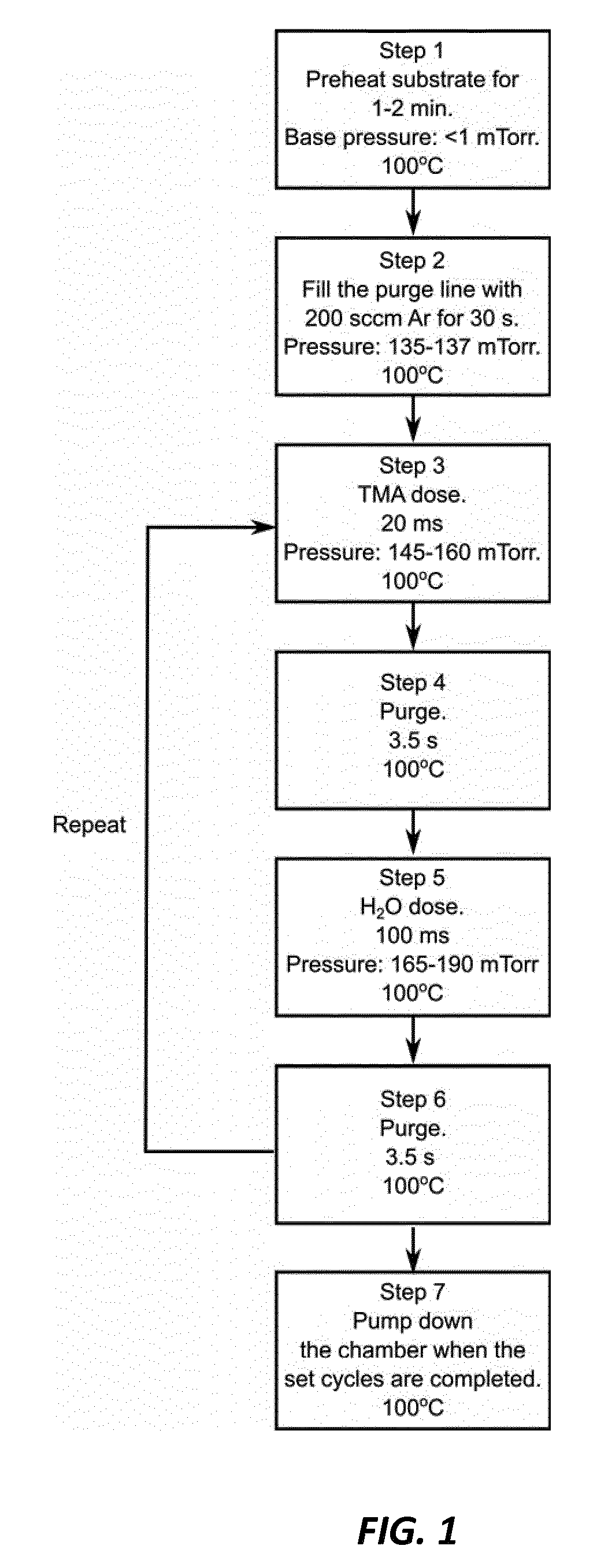
[0012] FIG. 1 shows a schematic drawing of exemplary ALD process for fabricating a passivating barrier layer in the hybrid organic-inorganic solar cell, according to one embodiment of the invention.
[0013] FIGS. 2A-2C show X-ray diffraction (XRD) spectra of the perovskite film with and without the Al.sub.2O.sub.3 contacting passivating barrier layer immediately after fabrication (day 0) (2A), without a passivating barrier layer (2B), and (2C) with a passivating barrier layer, according to one embodiment of the invention.
[0014] FIGS. 3A-3O show schematic drawings of passivating barrier layers deposited in hybrid organic-inorganic p-i-n and n-i-p solar cells, according to embodiments of the current invention.
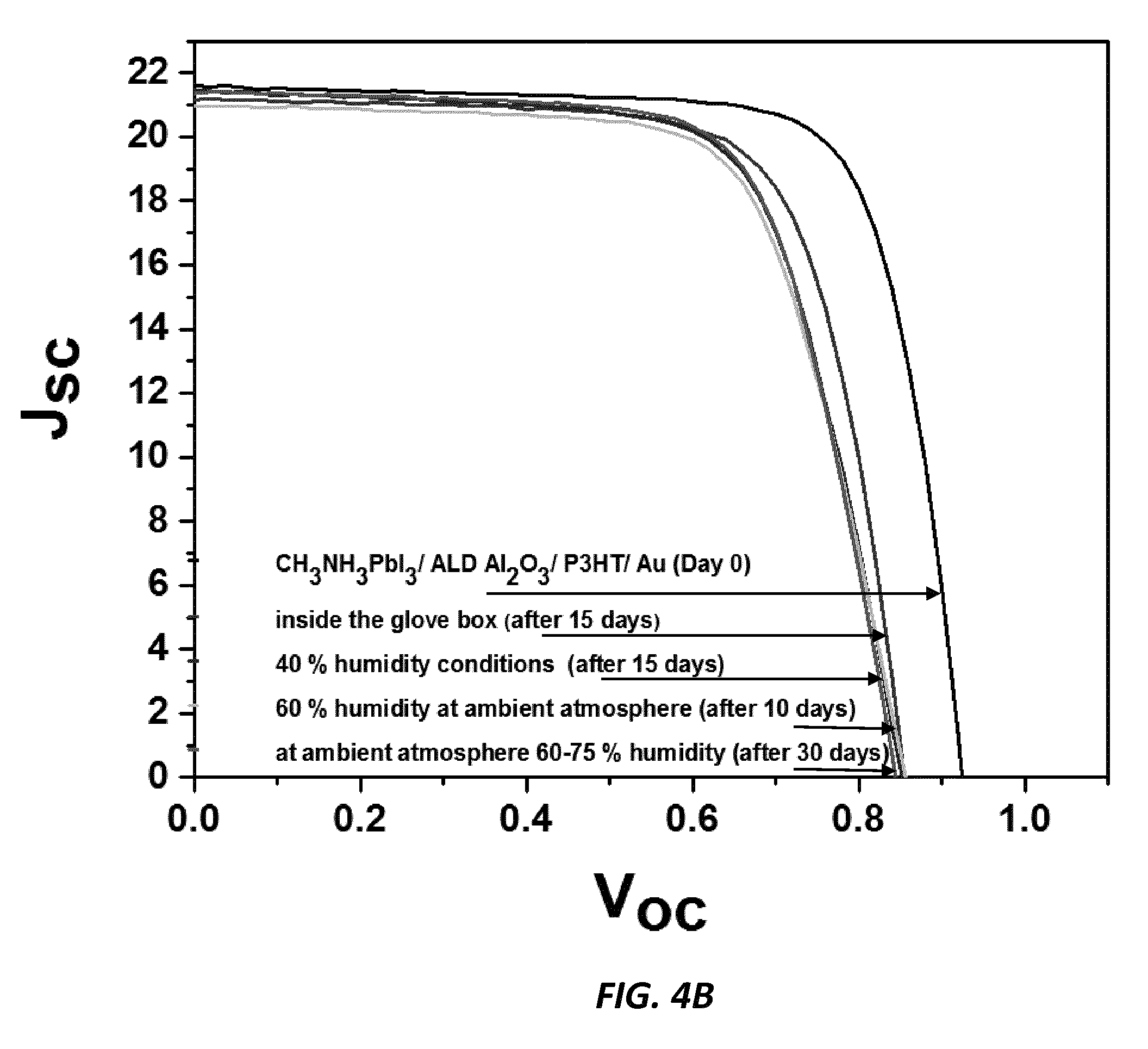
[0015] FIG. 4A shows experimental data of degradation without the Al.sub.2O.sub.3 contacting passivating barrier layer.
[0016] FIG. 4B shows experimental data of reduced degradation with the Al.sub.2O.sub.3 contacting passivating barrier layer, according to one embodiment of the invention.
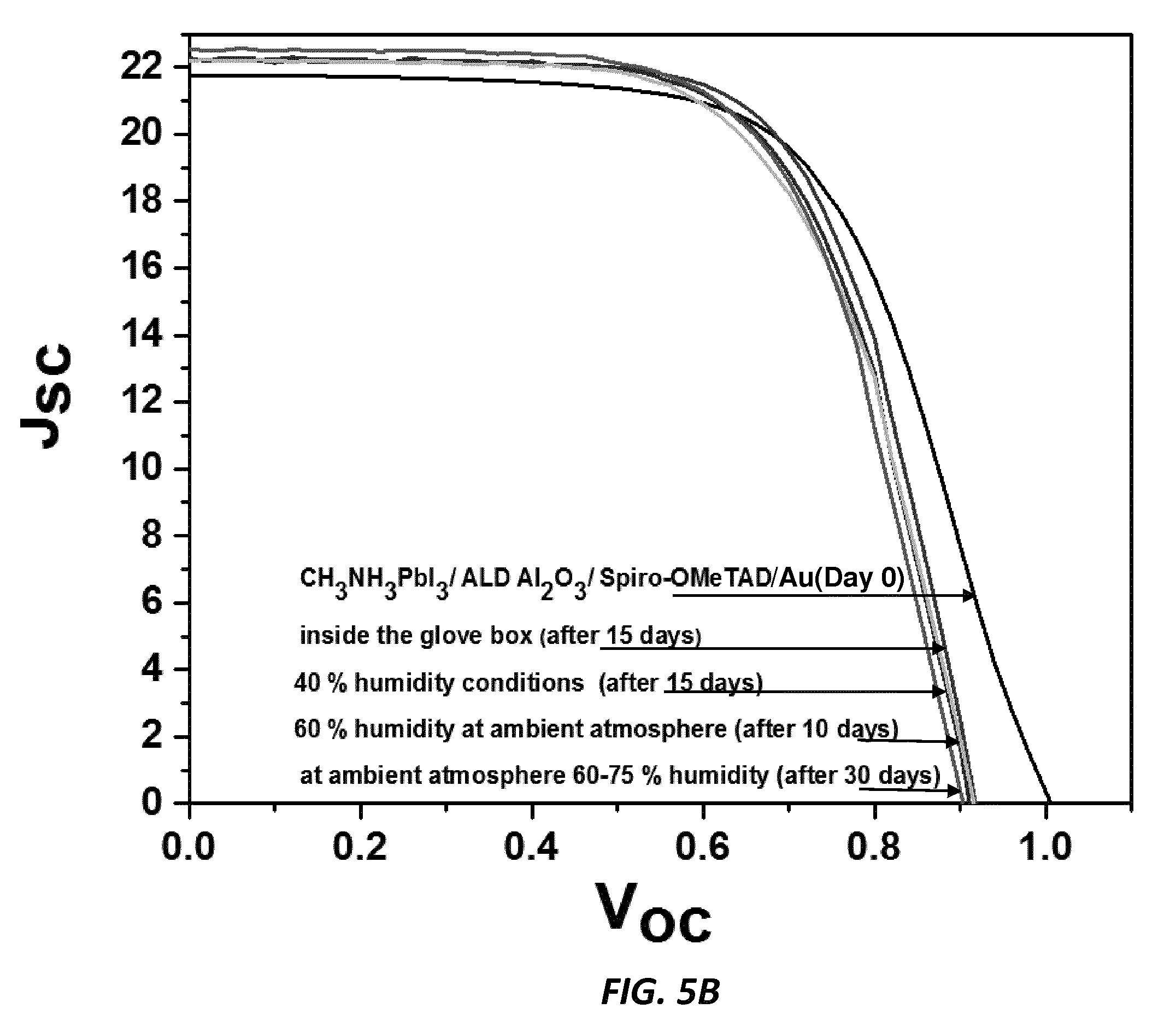
[0017] FIG. 5A shows experimental data of degradation without the Al.sub.2O.sub.3 contacting passivating barrier layer.
[0018] FIG. 5B shows experimental data of reduced degradation with the Al.sub.2O.sub.3 contacting passivating barrier layer, according to one embodiment of the invention.
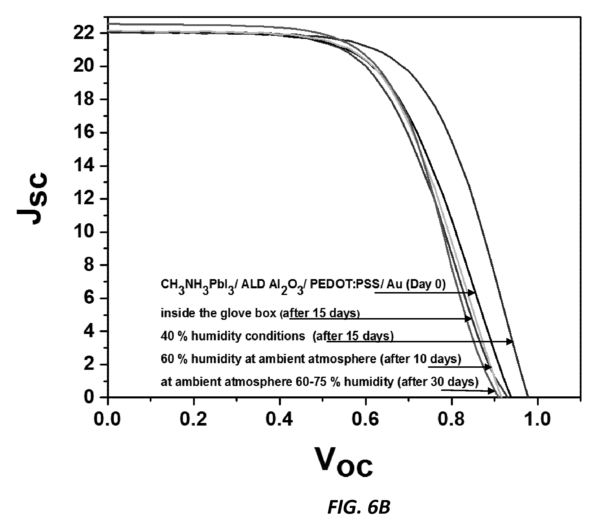
[0019] FIG. 6A compares the cell performance with and without the Al.sub.2O.sub.3 contacting passivating barrier layer immediately after fabrication (day 0), according to one embodiment of the invention.
[0020] FIG. 6B shows virtually no degradation with the Al.sub.2O.sub.3 contacting passivating barrier layer, according to one embodiment of the invention.
DETAILED DESCRIPTION
[0021] The current invention provides improved devices and processes for fabricating at least one passivating barrier layer in perovskite solar cells and demonstrate superior performance.
[0022] Thus the problem of high instability of hybrid organic-inorganic IV-halide perovskite solar cells is successfully addressed.
[0023] According to one example of the invention, a thin (e.g., between 0.2 nm and several nanometers thick) Al.sub.2O.sub.3 passivating barrier layer is used to seal off the sensitive perovskite layer. This layer protects the perovskite layer during further deposition of electron selective or hole selective contact layers as well as over the lifetime of the operational solar cell device against water, water vapor, and oxygen, yet it does not prevent the formation of a low-resistance contact to the perovskite layer. Here the Al.sub.2O.sub.3 passivating barrier layer is sufficiently thin that it provides a tunnel contact for the solar cell. This layer is preferably deposited using atomic layer deposition (ALD), from trimethylaluminum (TMA) and H.sub.2O at 100.degree. C. An exemplary ALD process for this is schematically depicted in FIG. 1. In this example we used 4 ALD deposition cycles. Preferably the number of ALD cycles is from 1 to 10, and more preferably the number of ALD cycles is from 5 to 10.
[0024] X-ray diffraction (XRD) spectra of the perovskite film with and without ALD Al.sub.2O.sub.3 on top are shown in FIG. 2A. There is no obvious change in the crystalline structure of the perovskite film before and after the deposition of ALD Al.sub.2O.sub.3 on top as confirmed by the characteristic peaks (14.10, 28.4.degree. and 43.2.degree.) present in both the respective spectra, and can be assigned to the (110), (220), and (330) peaks of the CH.sub.3NH.sub.3PbI.sub.3. After exposure to humidity, the degradation of the perovskite without the ALD Al.sub.2O.sub.3 passivating barrier layer on top is seen from the appearance of a new peak at 12.6.degree. in the XRD spectra of FIG. 2B. This peak is assigned to the (001) diffraction peak of Pb.sub.2, which is formed as a result of the decomposition of the perovskite when exposed to oxygen and moisture. On the contrary, there is no appearance of this signature 12.6.degree. peak of PbI.sub.2 in the XRD spectra of the perovskite with ALD Al.sub.2O.sub.3 on top (FIG. 2C) when exposed to the same humidity conditions, which confirms that the ALD Al.sub.2O.sub.3 contacting the perovskite serves as a passivating barrier layer and enhances its stability.
[0025] Complete solar cell devices have been fabricated. FIGS. 3A-3O show exemplary embodiments of a hybrid organic-inorganic solar cell that include a substrate, a transparent conductive oxide (TCO) layer deposited on the substrate, an electron transport material (ETM) layer, where the ETM layer is an n-type layer, a hole transport material (HTM) layer, where the HTM is a p-type layer, at least one passivating barrier layer, a perovskite layer, where the perovskite layer is an i-type layer, and an electrode layer where the substrate, the TCO layer, the ETM layer, the perovskite layer, the HTM layer and the electrode layer are arranged in an n-i-p stack, or the substrate, the TCO layer, the HTM layer, the perovskite layer, the ETM layer and the electrode layer are arranged in a p-i-n stack, where the at least one passivating barrier layer is disposed (i) between the perovskite layer and the HTM layer, or (ii) between the perovskite and the ETM layer, or (iii) between the perovskite and the HTM layer, and between the perovskite layer and the ETM, or (iv) between the TCO layer and the ETM layer, and between the ETM layer and the perovskite layer, and between the perovskite layer and the HTM layer, or (v) between the substrate and the TCO layer, and between the TCO layer and the ETM layer, and between ETM layer and the perovskite layer, and between the perovskite layer and the HTM layer, or (vi) between a pair of the ETM layers, or (vii) between a pair of the HTM layers.
[0026] Experiments to date relate to the configuration of FIG. 3A-3B (passivating barrier layers between perovskite and hole transport material (HTM) shown in both p-i-n and n-i-p configurations), although the configurations of FIG. 3C-3D (passivating barrier layers between perovskite and electron transport material (ETM) shown in both p-i-n and n-i-p configurations) and FIG. 3E-3F (barriers layers between perovskite and HTM and between perovskite and ETM shown in both p-i-n and n-i-p configurations) are also possible. Here an important feature of all examples is that the passivating barrier layer is directly on the photoactive perovskite layer. FIGS. 3G-3N show passivating barrier layers between multiple layers of the hybrid organic-inorganic p-i-n and n-i-p solar cells, according to embodiments of the invention. The perovskite solar cell contains two electrodes of which at least one should be transparent. One of the electrodes can therefore be non-transparent. FIG. 3O shows a solar cell stack having a transparent conducting oxide layer that is distal to the substrate layer and a non-transparent or semi-transparent electrode that is proximal to the substrate layer.
[0027] In a further aspect of the invention, the electrode close to the substrate can therefore also be semi-transparent on non-transparent. In the FIGS. 3A-3L, the TCO is always close to the substrate. However, if the top electrode is transparent, the electrode close to the substrate can be non-transparent.
[0028] According to one aspect of the current invention, the ETM layer material includes Fullerene, ZnOS, TiO.sub.2, SnO.sub.2, ZnO, CdS, Sb.sub.2S.sub.3, Bi.sub.2S.sub.3, or any combination thereof. Here the Fullerene includes PCBM, or C60, where the Fullerene is doped or undoped.
[0029] In another aspect of the invention, the HTM layer material includes P3HT, Spiro-OMeTAD, PEDOT:PSS, NiO.sub.x, MoO.sub.x, WO.sub.x, CuO.sub.x, CuSCN, V.sub.2O.sub.5, MoS.sub.2, CuGaO.sub.2, PTAA, Poly-TPD, PbS, or any combination thereof. Here the P3HT, Spiro-OMeTAD, PTAA, and Poly-TPD are doped or undoped.
[0030] In a further aspect of the invention, the TCO layer material includes In.sub.2O.sub.3:SnO.sub.2 (ITO), In.sub.2O.sub.3:H, SnO.sub.2:F (FTO), SnO.sub.2, ZnO:Al, or ZnO:B, or any combination thereof.
[0031] In yet another aspect of the invention, the electrode layer material includes In.sub.2O.sub.3:SnO.sub.2 (ITO), In.sub.2O.sub.3:H, ZnO:Al, ZnO:B, SnO.sub.2, C, Au, Ag, Cu, Ni, or Al.
[0032] According to one aspect of the invention, the passivating barrier layer material includes of Al.sub.2O.sub.3, SnO.sub.2, TiO.sub.2, ZnO, NiO, MoO3, CuO, CuGaO.sub.2, Y.sub.2O.sub.3, SiN.sub.x, SiO.sub.2, Ta.sub.2O.sub.5, Triflurorobutylamine hydroiodide (TFBA), AlF.sub.x, LiF, or PbI.sub.2.
[0033] In a further aspect of the invention, the perovskite layer material includes CH.sub.3NH.sub.3PbI.sub.3, CH.sub.3NH.sub.3PbCl.sub.3, CH.sub.3NH.sub.3PbBr.sub.3, CH.sub.3NH.sub.3PbI.sub.3-xCl, CH.sub.3NH.sub.3PbI.sub.3-xBr.sub.x, HC(NH.sub.2).sub.2PbI.sub.3, HC(NH.sub.2).sub.2PbCl.sub.3, HC(NH.sub.2).sub.2PbBr.sub.3, HC(NH.sub.2).sub.2PbI.sub.3-xCl, HC(NH.sub.2).sub.2PbI.sub.3-xBr.sub.x, [HC(NH.sub.2).sub.2].sub.1-xCs.sub.xPbI.sub.3, [HC(NH.sub.2).sub.2].sub.1-xCs.sub.xPbI.sub.3-yBr.sub.y, CsPbI.sub.3-xBr.sub.x, CH.sub.3NH.sub.3Pb.sub.1-xSn.sub.xI.sub.3-yBr.sub.y, (CH.sub.3NH.sub.3).sub.1-x-y[HC(NH.sub.2).sub.2].sub.yCs.sub.xPbI.sub.3-z- Br.sub.z, (CH.sub.3NH.sub.3).sub.1-x-y[HC(NH.sub.2).sub.2].sub.yCs.sub.xPb- .sub.1-zSn.sub.zI.sub.3-.delta.Br.sub..delta., and (CH.sub.3NH.sub.3).sub.1-x-y-z[HC(NH.sub.2).sub.2].sub.zCs.sub.yRb.sub.xP- bI.sub.3-.delta.Br.sub..delta.. In one aspect the Pb of the perovskite is partially or completely replaced by other group IV elements.
[0034] In a first example, poly(3-hexylthiophene) (P3HT) is used as the hole transport material. FIG. 4A shows degradation without the Al.sub.2O.sub.3 contacting passivating barrier layer. FIG. 4B shows reduced degradation with the Al.sub.2O.sub.3 contacting passivating barrier layer.
[0035] In a second example, 2,2',7,7'-tetrakis(N,N-di-p-methoxyphenyl-amine)9,9'-spirobifluorene (Spiro-OMeTAD) is used as the hole transport material. FIG. 5A shows degradation without the Al.sub.2O.sub.3 contacting passivating barrier layer. FIG. 5B shows reduced degradation with the Al.sub.2O.sub.3 contacting passivating barrier layer.
[0036] In a third example, poly(3,4-ethylenedioxythiophene):poly(styrene sulfonate (PEDOT:PSS) is used as the hole transport material. FIG. 6A compares the cell performance with and without the Al.sub.2O.sub.3 contacting passivating barrier layer immediately after fabrication (day 0). It is seen that without the use of the Al.sub.2O.sub.3 contacting passivating barrier layer, the cells cannot properly be fabricated. Using the Al.sub.2O.sub.3 contacting passivating barrier layer the cells have good initial I-V performance. Moreover, in FIG. 6B it is shown that there is virtually no degradation with the Al.sub.2O.sub.3 contacting passivating barrier layer. In the case of PEDOT:PSS as the HTM, the Al.sub.2O.sub.3 layer not only protects the device from humidity, but it is also important to enable the processing of perovskite cells using PEDOT:PSS as the HTM.
[0037] In all cases, there is no deterioration of initial cell efficiencies when the Al.sub.2O.sub.3 passivating barrier layer is used compared to the cells without the Al.sub.2O.sub.3 passivating barrier layer. Cells were exposed to 40% humidity atmospheric conditions for 15 days, then to 60% humidity for 10 more days, and then to ambient laboratory atmosphere (60-75% humidity) for 30 more days. Greatly improved stability of the devices under humid conditions is provided by the passivating barrier layers. The I-V performance is retained in the structures having the passivating barrier layer, while performance of cells without the passivating barrier layer degrades severely over time.
[0038] The present invention has now been described in accordance with several exemplary embodiments, which are intended to be illustrative in all aspects, rather than restrictive. Thus, the present invention is capable of many variations in detailed implementation, which may be derived from the description contained herein by a person of ordinary skill in the art. For example the ETM (or HTM) has preferably three main functions:
1. good electron transport (good hole transport); 2. good hole blocking properties (good electron blocking properties); and 3. barrier properties that include passivation functionality, and chemical diffusion barrier functionality. Here, the passivation functionality (i.e. a chemical reaction or physisorption with reactive species with neighboring layer(s)), where this functionality can have two effects: (i) reducing bulk and/or interface recombination, which applies to the perovskite layer and the interface of the perovskite with a neighboring layer, and (ii) preventing degradation reactions involving the above mentioned reactive species, which applies to any of the layers in the stack.
[0039] Further, the chemical diffusion barrier functionality includes protection against H.sub.2O, CO.sub.2, O.sub.2, solvents, decomposition materials of other layers (e.g. MAI, etc.).
[0040] Further, the above-mentioned properties can be realized in several layers: e.g. the ETM may consist of: 1 electron transport layer, 1 hole blocking layer, 1 passivating barrier layer. However, it is also possible to combine 2 or 3 properties in a single layer. Of course, more passivating barrier layers can be introduced to protect the layers constituting the ETM, HTM, TCO and electrode. Therefore the barrier can be placed on different locations as depicted in the many device stacks.
[0041] All such variations are considered to be within the scope and spirit of the present invention as defined by the following claims and their legal equivalents.
* * * * *
D00000
D00001
D00002
D00003
D00004
D00005
D00006
D00007
D00008
D00009
D00010
D00011
D00012

D00013
D00014

D00015
D00016

D00017
XML
uspto.report is an independent third-party trademark research tool that is not affiliated, endorsed, or sponsored by the United States Patent and Trademark Office (USPTO) or any other governmental organization. The information provided by uspto.report is based on publicly available data at the time of writing and is intended for informational purposes only.
While we strive to provide accurate and up-to-date information, we do not guarantee the accuracy, completeness, reliability, or suitability of the information displayed on this site. The use of this site is at your own risk. Any reliance you place on such information is therefore strictly at your own risk.
All official trademark data, including owner information, should be verified by visiting the official USPTO website at www.uspto.gov. This site is not intended to replace professional legal advice and should not be used as a substitute for consulting with a legal professional who is knowledgeable about trademark law.