Shunt Resistor Mounting Structure And Mounting Board
NAKAMURA; Keishi ; et al.
U.S. patent application number 16/313381 was filed with the patent office on 2019-07-25 for shunt resistor mounting structure and mounting board. The applicant listed for this patent is KOA CORPORATION. Invention is credited to Keishi NAKAMURA, Susumu TOYODA.
| Application Number | 20190227104 16/313381 |
| Document ID | / |
| Family ID | 60785412 |
| Filed Date | 2019-07-25 |


| United States Patent Application | 20190227104 |
| Kind Code | A1 |
| NAKAMURA; Keishi ; et al. | July 25, 2019 |
SHUNT RESISTOR MOUNTING STRUCTURE AND MOUNTING BOARD
Abstract
A shunt resistor mounting structure comprising: a resistor including a pair of terminal portions and adapted to perform current sensing; and a mounting board. The mounting board includes: a mounting portion including a pair of a first land and a second land to which the pair of terminal portions are respectively connected, and which allow a current to be measured to flow through the resistor; a substrate having the pair of lands formed thereon; a first voltage terminal formed on the substrate and including a line pattern led out from the first land; and a second voltage terminal including a wire connected to the terminal portion corresponding to the second land.
| Inventors: | NAKAMURA; Keishi; (Nagano, JP) ; TOYODA; Susumu; (Nagano, JP) | ||||||||||
| Applicant: |
|
||||||||||
|---|---|---|---|---|---|---|---|---|---|---|---|
| Family ID: | 60785412 | ||||||||||
| Appl. No.: | 16/313381 | ||||||||||
| Filed: | May 25, 2017 | ||||||||||
| PCT Filed: | May 25, 2017 | ||||||||||
| PCT NO: | PCT/JP2017/019499 | ||||||||||
| 371 Date: | December 26, 2018 |
| Current U.S. Class: | 1/1 |
| Current CPC Class: | G01R 15/00 20130101; G01R 19/0092 20130101 |
| International Class: | G01R 19/00 20060101 G01R019/00 |
Foreign Application Data
| Date | Code | Application Number |
|---|---|---|
| Jun 27, 2016 | JP | 2016-126805 |
Claims
1. A shunt resistor mounting structure comprising: a resistor including a pair of terminal portions and adapted to perform current sensing; and a mounting board, the mounting board including: a mounting portion including a pair of a first land and a second land to which the pair of terminal portions are respectively connected, and which allow a current to be measured to flow through the resistor; a substrate having the pair of lands formed thereon; a first voltage terminal formed on the substrate and connected by a lead-out line portion led out from the first land; and a second voltage terminal connected by a wire from the second land.
2. The shunt resistor mounting structure according to claim 1, wherein the lead-out line portion and the wire intersect each other in a plan view of the substrate.
3. The shunt resistor mounting structure according to claim 1, wherein the lead-out line portion is led out from a side portion of the first land.
4. The shunt resistor mounting structure according to claim 1, wherein the terminals of the resistor are formed with an alloy plating film.
5. A shunt resistor mounting board for mounting a resistor having a pair of terminal portions and adapted to perform current sensing, the mounting board comprising: a mounting portion including a pair of a first land and a second land to which the pair of terminal portions are respectively connected, and which allow a current to be measured to flow through the resistor; a substrate having the pair of lands formed thereon; a first voltage terminal formed on the substrate and connected by a lead-out line portion led out from the first land; and a second voltage terminal formed away from the second land.
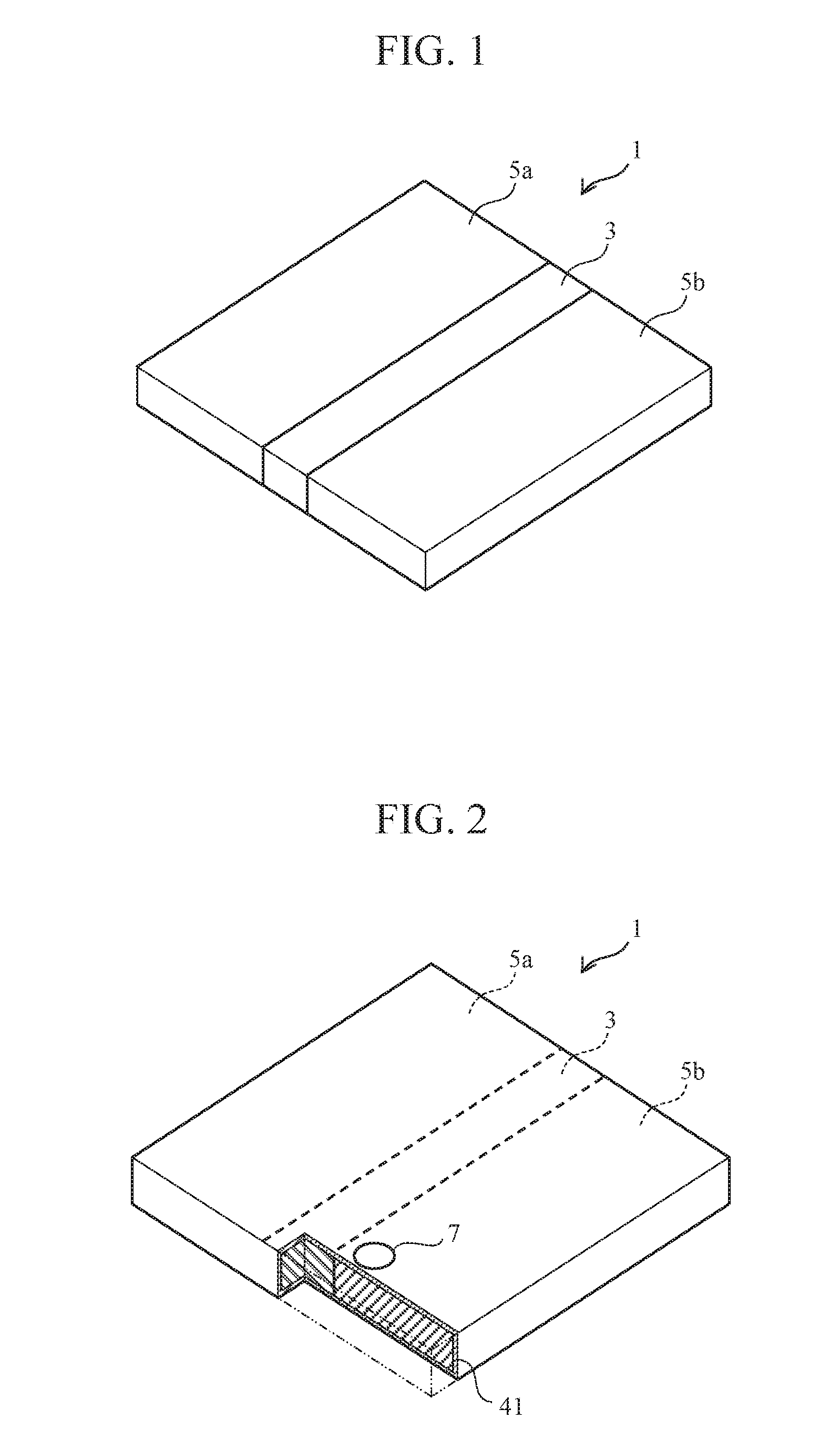
Description
TECHNICAL FIELD
[0001] The present invention relates to a mounting structure and the like for a shunt resistor for sensing current.
BACKGROUND ART
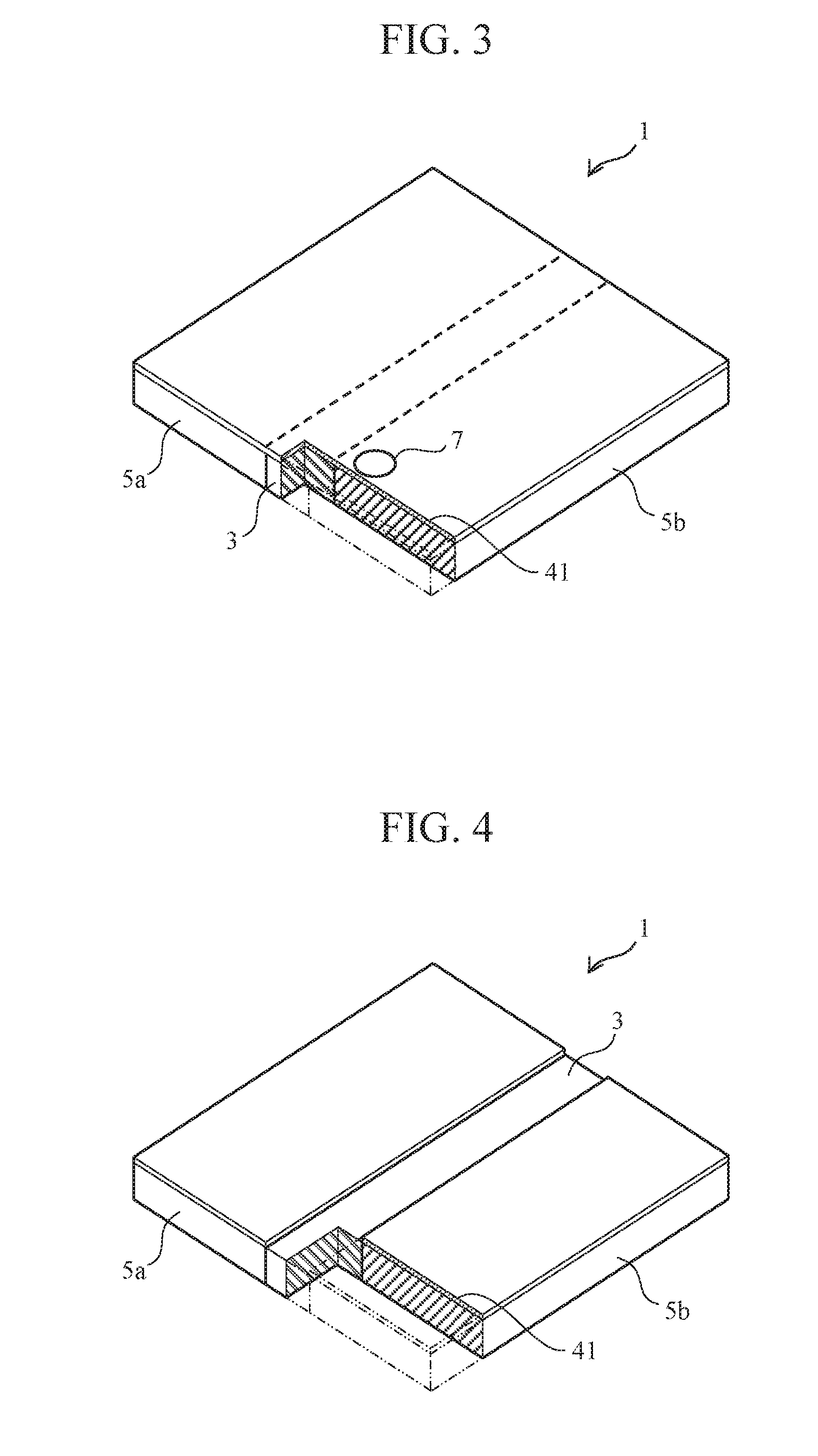
[0002] Conventionally, a current sensing device is known in which a current to be monitored is flowed through a shunt resistor, a voltage between the electrodes at the ends of the resistor is measured, and the current is sensed using a known resistance value. When the current sensing device is used to sense a current flowing through the resistor that includes a high frequency component, a slight parasitic inductance of the resistor introduces an error into the sensed value.
[0003] FIG. 14 is a plan view illustrating an example of a general current sensing device X. The current sensing device X includes a board 111 having disposed thereon: lines (current terminals) 117a, 117b including a first land and a second land; and sensing line patterns 125, 127 (voltage sensing terminals) which are led out from within a gap 121 between the lines 117a, 117b to the outside of the gap 121 by means of lead-out line portions 125a, 127a. The terminals of a shunt resistor 101 are connected to the first land and the second land.
[0004] In the above configuration, a parasitic inductance of the resistive element (the length of the resistive element, i.e., electrode to electrode distance) causes a voltage corresponding to a temporal change in the current to be measured, resulting in an error corresponding to the voltage.
[0005] Accordingly, in Patent Literature 1, for example, line patterns which are connected to voltage sensing terminals and disposed on a board are arranged in the same direction as the direction of flow of a current to be sensed, and are also provided with a certain length, so that mutual inductance is caused between the line patterns and a resistive element in that portion. In this way, an induced voltage due to the inductance of the resistive element is cancelled, thereby reducing a sensing error caused by the induced voltage of the resistive element as seen from the measuring system.
[0006] Patent Literature 2 discloses a resistor mounted structure which includes a board for mounting a shunt resistor, a pair of lands formed on the board and adapted to flow a current through the resistor 1, and a pair of wire connection portions which are formed on the board and connected to the resistor via wires. The pair of wire connection portions are respectively arranged laterally of the resistor between the pair of lands. One wire is connected, over and across a voltage sensing line or an extension thereof to which the other wire is connected, between a voltage sensing position of the resistor and the wire connection portion at the tip of the voltage sensing line.
CITATION LIST
Patent Literature
[0007] Patent Literature 1: JP 2002-372551 A
[0008] Patent Literature 2: JP 2012-233706 A
SUMMARY OF INVENTION
Technical Problem
[0009] However, the technique according to Patent Literature 1 leads to a complex structure and an increase in the number of manufacturing steps.
[0010] The technique according to Patent Literature 2 may make it difficult to perform a wire forming step.
[0011] An object of the present invention is to provide a shunt resistor mounting structure with which it is possible to suppress, using a relatively simple structure, the influence of parasitic inductance due to the length of a resistive element.
Solution to Problem
[0012] According to an aspect of the present invention, there is provided a shunt resistor mounting structure including: a resistor having a pair of terminal portions and adapted to perform current sensing; and a mounting board. The mounting board includes: a mounting portion having a pair of a first land and a second land to which the pair of terminal portions are respectively connected, and which allow a current to be measured to flow through the resistor; a substrate having the pair of lands formed thereon; a first voltage terminal formed on the substrate and connected by a lead-out line portion led out from the first land; and a second voltage terminal connected by a wire from the second land.
[0013] By forming the connections between the lands and the voltage terminals using a lead-out line portion for one and a wire for the other, the wiring can be spatially separated.
[0014] Preferably, the lead-out line portion and the wire may intersect each other in a plan view of the substrate.
[0015] A crossing structure of line patterns can be simply formed, and the loop area of the sensing portion can be reduced.
[0016] Preferably, the lead-out line portion may be led out from a side portion of the first land. By leading out from the side portion, a finer pattern can be obtained.
[0017] Preferably, the terminals of the resistor may be formed with an alloy plating film.
[0018] According to another aspect of the present invention, there is provided a shunt resistor mounting board for mounting a resistor having a pair of terminal portions and adapted to perform current sensing, the mounting board including: a mounting portion including a pair of a first land and a second land to which the pair of terminal portions are respectively connected, and which allow a current to be measured to flow through the resistor; a substrate having the pair of lands formed thereon; a first voltage terminal formed on the substrate and connected by a lead-out line portion led out from the first land; and a second voltage terminal (for connection by wire) formed away from the second land.
[0019] The description includes the contents disclosed in Japanese Patent Application No. 2016-126805 from which the present application claims the priority.
Advantageous Effects of Invention
[0020] According to the present invention, a shunt resistor mounting structure can be provided with which the influence of parasitic inductance due to the length of a resistive element can be suppressed, using a relatively simple structure.
BRIEF DESCRIPTION OF THE DRAWINGS
[0021] FIG. 1 is a perspective view of a first configuration example of a shunt resistor.
[0022] FIG. 2 is a perspective view of a second configuration example of the shunt resistor.
[0023] FIG. 3 is a perspective view of a third configuration example of the shunt resistor.
[0024] FIG. 4 is a perspective view of a fourth configuration example of the shunt resistor.
[0025] FIG. 5 is a perspective view of a fifth configuration example of the shunt resistor.
[0026] FIG. 6 is a perspective view of a sixth configuration example of the shunt resistor.
[0027] FIG. 7A to FIG. 7D illustrate examples in which the electrodes of a shunt resistor partly protrude on the resistive element side to serve as a marker for a wire bonding position.
[0028] FIGS. 8A and 8B illustrate a configuration example of a shunt resistor mounting structure according to a first embodiment of the present invention.
[0029] FIG. 9 illustrates an example of a circuit configuration of a shunt resistor mounting structure corresponding to FIG. 8.
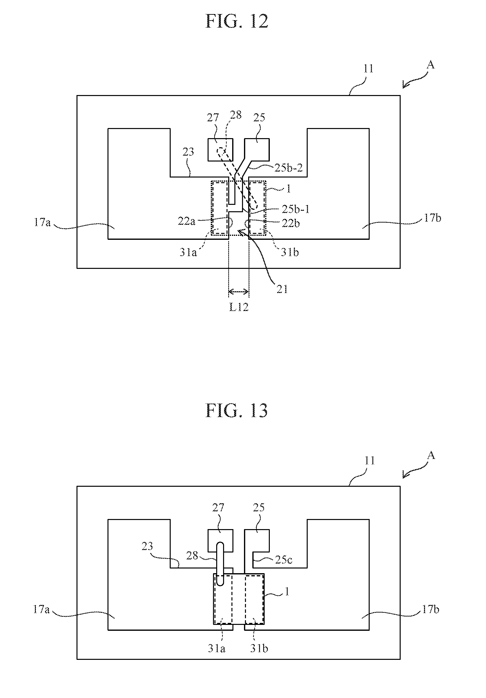
[0030] FIGS. 10A and 10B illustrate a shunt resistor mounting structure according to a second embodiment of the present invention, corresponding to FIGS. 8A and 8B.
[0031] FIGS. 11A and 11B show plan views comparatively illustrating a mounting structure according to the first or the second embodiment (FIG. 11A), and a general mounting structure (FIG. 11B).
[0032] FIG. 12 is a plan view of an example of a shunt resistor mounting structure according to a third embodiment of the present invention.
[0033] FIG. 13 is a plan view of an example of a shunt resistor mounting structure according to a fourth embodiment of the present invention.
[0034] FIG. 14 is a plan view of an example of a general current sensing device.
DETAILED DESCRIPTION OF THE PREFERRED EMBODIMENTS
[0035] In the following, with respect to a resistor mounting structure according to an embodiment of the present invention, a shunt resistor will be described by way of example, with reference to the drawings.
[0036] A configuration example of the shunt resistor used in the present embodiment will be described.
[0037] FIG. 1 is a perspective view of a first configuration example of the shunt resistor. The shunt resistor 1 has a butt joint structure in which a resistive element 3 and first and second electrodes (a pair of terminal portions) 5a, 5b are arranged with end surfaces abutting each other, for example. The resistive element 3 may employ a Cu--Ni-based, Ni--Cr-based, or Cu--Mn-based resistive material, for example. The electrodes 5a, 5b may employ a material such as Cu. The resistive element 3 and the electrodes 5a, 5b may be joined by welding using an electron beam, a laser beam and the like, by cladding, or by brazing using a metal nano paste. The shunt resistor may have a product size of 10.times.10.times.0.5 (mm), for example, and may have a resistance value of 0.1 m.OMEGA.. The shunt resistor 1 may have a structure that consists of the resistive material (i.e., not provided with electrodes of other metal material).
[0038] FIG. 2 is a perspective view of a second configuration example of the shunt resistor. The shunt resistor 1 of FIG. 2 has a configuration in which the resistor 1 of FIG. 1 has an entirely plated structure. A plating film 41 may be used for surface treatment for facilitating wire bonding. The plating film 41 comprises alloy plating, such as Ni--P plating or Ni--P--W plating, and may employ a material having a resistivity greater than that of at least the Cu of the electrodes. The plating film 41 is formed by electrolytic plating or electroless plating.
[0039] While in FIG. 2, the boundary between the resistive element 3 and the electrode 5b is indicated by a dashed line, the boundary becomes difficult to see after plating is performed. Accordingly, the electrode is provided with a mark 7 near the boundary. The mark 7 is an example of a marking indication for determining the position for wire bonding to be performed in a subsequent step, as will be described later.
[0040] In an example of the process to provide the mark, the electrode 5b is initially provided with a dent using a punch and the like. Then, the plating film 41 is formed, thereby leaving the dent as a marker.
[0041] FIG. 3 is a perspective view of a third configuration example of the shunt resistor. The shunt resistor 1 of FIG. 3 has a configuration in which only the upper surface of the shunt resistor 1 is plated, for example. That is, the plating film 41 is not provided on the side surfaces or the lower surface. Because the upper surface is provided with the plating film 41, the mark 7 can be formed on the upper surface as an effective marker for positioning during wire bonding.
[0042] FIG. 4 is a perspective view of a fourth configuration example of the shunt resistor. The shunt resistor 1 of FIG. 4 has a configuration in which only the upper surfaces of the electrodes 5a, 5b are plated, for example. That is, the plating film 41 is not provided on the side surfaces, the lower surface, or the resistive element 3. Because the plating film 41 is provided on the upper surfaces of the electrodes 5a, 5b, a height difference corresponding to the thickness of the plating film 41 serves as a marker. Accordingly, in contrast to FIG. 3, it is possible to easily determine the position for wire bonding even without newly forming a mark.
[0043] FIG. 5 is a perspective view of a fifth configuration example of the shunt resistor. The shunt resistor 1 of FIG. 5 has a configuration in which the exposed portions of the electrodes 5a, 5b are plated, for example. The plating film 41 is not formed on the surface of the resistive element 3.
[0044] Because the plating film 41 is provided on the upper surfaces of the electrodes 5a, 5b, the height difference corresponding to the thickness of the plating film 41 serves as a marker. Accordingly, in contrast to FIG. 3, it is also possible in this structure to easily determine the position for wire bonding, even without newly forming a mark.
[0045] Variations of the location for plating have been described with reference to FIG. 2 to FIG. 5. However, in terms of achieving the effect of facilitating wire bonding, plating may be provided only in a region including the position for wire bonding or the vicinity thereof.
[0046] FIG. 6 is a perspective view of a sixth configuration example of the shunt resistor. The shunt resistor 1a of FIG. 6 has a configuration in which, for example, one electrode 5a and the other electrode 5b have a height difference .DELTA.h. In this example, the height difference is formed by bending the one electrode 5a. The significance of forming the height difference will be described later.
[0047] FIG. 7A to FIG. 7D illustrate examples in which the electrodes 5a, 5b of the shunt resistor 1 partly protrude on the resistive element 3 side to provide a marker for the wire bonding position. FIG. 7A illustrates an example in which a protruding portion 9 is only formed in one electrode 5b. FIG. 7B illustrates an example in which protruding portions 9a, 9b are formed in both electrodes 5a, 5b. FIG. 7C is an example in which only one electrode 5b is formed with a protruding portion 9c, where the position of the protruding portion is displaced toward one end in a direction in which the joined portion of the electrode and the resistive element is formed. FIG. 7D illustrates an example in which the protruding portion 9c of FIG. 7C is moved toward one side surface, forming a protruding portion 9d, where one end of the protruding portion 9d and one end of the resistor 1 are aligned.
[0048] Thus, it is also possible to provide the marker for the wire bonding position by providing any of the protruding portions 9a to 9d.
[0049] The shunt resistor may have a configuration in which the shunt resistor consists of the resistive element and is not provided with the electrode terminals.
[0050] The mounting structure for the shunt resistor described above by way of example will be described in detail.
First Embodiment
[0051] FIG. 8 illustrates a configuration example of the shunt resistor mounting structure according to a first embodiment of the present invention. FIG. 8A is a perspective view illustrating the configuration before the shunt resistor is mounted. FIG. 8B is a perspective view illustrating the configuration after the shunt resistor is mounted.
[0052] As illustrated in FIG. 8, the shunt resistor mounting structure according to the present embodiment includes one of the shunt resistors 1 described above with reference to FIG. 1 to FIG. 5 and FIG. 7, and a mounting board A for mounting the shunt resistor 1.
[0053] The shunt resistor 1 is a resistor which is provided with, e.g., a pair of terminal portions (first and second electrodes) 5a, 5b described above, and adapted for sensing current.
[0054] FIG. 9 illustrates an example of the circuit configuration of a shunt resistor mounting structure corresponding to FIG. 8.
[0055] The mounting structure (current sensing module) B illustrated in FIG. 9 includes, for example, the shunt resistor 1 and the mounting board A illustrated in FIG. 8, which includes (not illustrated in FIG. 8) an amplifier 63 for amplifying a voltage signal between the terminals 5a, 5b of the shunt resistor 1, an A/D converter 65 for A/D converting the signal amplified by the amplifier 63, and a microcomputer 67 for receiving a digital signal output and performing computation.
[0056] Upon energization, a voltage value acquired from a lead-out line portion 25a and the wire 28 of the shunt resistor 1 is amplified and converted into digital data, and a current value is computed by the microcomputer 67. The current value is sent to various electric devices via a data bus and the like.
[0057] The mounting board A includes a board (substrate) 11 comprising a glass epoxy board, for example, and a first line pattern 17a and a second line pattern 17b which are formed of electrically conductive patterns of copper foil and the like, for example, on one surface of the board 11.
[0058] Manufacturing steps will be described briefly.
[0059] 1) The line patterns of copper foil and the like are formed on one surface of the substrate 11 by etching, for example.
[0060] 2) Optionally, a resist film and the like may be used to open a mounting region and the like while covering the rest.
[0061] 3) The resistor is placed (see FIG. 8A, L1), whereby one is wired.
[0062] 4) The other is connected (wire 28) by wire bonding.
[0063] The first line pattern 17a and the second line pattern 17b are respectively electrically connected to the pair of terminal portions 5a, 5b of the shunt resistor 1, so that a current to be measured can flow through the shunt resistor 1. The locations of the line patterns 17a, 17b to which the terminal portions 5a, 5b are connected are herein referred to as a pair of lands 31a, 31b.
[0064] The pair of lands 31a, 31b are spaced apart from each other, with a gap 21 of a distance L11 provided between respective proximate end surfaces 22a, 22b thereof opposing each other. A region 31 in FIG. 8B forms a mounting portion for the shunt resistor 1. The pair of lands (first land) 31a, 31b and the pair of electrodes (terminal portions) 5a, 5b of the shunt resistor 1 are respectively connected by soldering and the like.
[0065] Further, in the mounting board A, the substrate 11 is provided with: a second voltage terminal 27 disposed at a position which is substantially opposite the first land 31a and spaced apart from a side portion 23 of the first line pattern 17a in a direction in which the gap 21 extends; and a first voltage terminal 25 disposed at a position which is substantially opposite the second land 31b and spaced apart from the side portion 23 of the second line pattern 17b in the direction in which the gap 21 extends.
[0066] The substrate 11 is also provided with a lead-out line portion 25a extending diagonally from the first land 31a to the first voltage terminal 25. Further, a wire 28 made of metal, for example, is provided connecting the second land 31b and the second voltage terminal 27. The wire 28 may be formed by wire bonding, for example. The voltage terminals 25, 27 are electrically connected (not illustrated) to the amplifier 63, for example.
[0067] As illustrated in FIG. 8B, the lead-out line portion 25a and the wire 28 intersect each other in a plan view of the substrate 11. The wire 28 is disposed above the surface of the substrate 11, so that the lead-out line portion 25a and the wire 28 can be spatially separated from each other in a direction normal to the surface of the substrate 11.
[0068] Thus, with the shunt resistor mounting structure according to the present embodiment, it is possible to suppress the influence of parasitic inductance of the resistive element, using a relatively simple structure. The crossing structure of the line patterns can be formed simply, and the loop area of the sensing portion can be reduced, enabling an improvement in current sensing accuracy. One line is provided by board wiring, while the other is provided by wiring using a wire, so that the mounting patterns can also be reduced in size.
[0069] In addition, compared to when two locations are wire-bonded, only one location needs to be subjected to wire bonding, thus simplifying the manufacturing process.
Second Embodiment
[0070] The shunt resistor mounting structure according to a second embodiment of the present invention will be described. FIGS. 10A and 10B illustrate the shunt resistor mounting structure according to the present embodiment, respectively corresponding to FIGS. 8A and 8B.
[0071] FIG. 8 and FIG. 10 differ in that on the mounting board A of the mounting structure illustrated in FIG. 10, an electronic component 31, such as a semiconductor component or a metal component (including a resistive element and the like), is mounted on the second line pattern 17b.
[0072] When the shunt resistor is mounted on the mounting board A, the shunt resistor 1a illustrated in FIG. 6 may be used. One terminal 5b of the shunt resistor 1a is connected to a region 33 on the electronic component 31 side by soldering, for example. As also illustrated in FIG. 6, by substantially matching the height difference (.DELTA.h) between one electrode 5a and the other electrode 5b of the shunt resistor 1a with the thickness of the electronic component, it becomes possible to arrange the shunt resistor 1a horizontally with respect to a major surface of the mounting board A. The effect of suppressing the influence of parasitic inductance of the resistive element is the same as in the first embodiment.
Summary of Advantages of First and Second Embodiments
[0073] FIG. 11 shows plan views comparatively illustrating the mounting structure according to the first or the second embodiment (FIG. 11A) and a general mounting structure (FIG. 11B). In the mounting structure illustrated in FIG. 11B, the first voltage terminal 25 and the second voltage terminal 27 are respectively led out from the first line pattern 17a and the second line pattern 17b by means of lead-out line portions 25c, 25d. Accordingly, a measurement error due to a magnetic flux inductance generated in a region indicated by sign AR1 cannot be disregarded.
[0074] Comparing FIG. 11A with FIG. 11B, in the structure of FIG. 11A corresponding to the present embodiment, the lead-out lines intersect each other in a spatially separated manner. In this way, the measurement error due to the magnetic flux inductance can be suppressed.
Third Embodiment
[0075] The shunt resistor mounting structure according to a third embodiment of the present invention will be described.
[0076] FIG. 12 is a plan view of an example of the shunt resistor mounting structure according to the present embodiment.
[0077] As will be seen by comparing with FIG. 8, in the mounting structure illustrated in FIG. 12, a lead-out line portion 25b connecting the first land 31a and the first voltage terminal 25 includes a first section 25b-1 substantially parallel with the end surface 22a, and a diagonally extending second section 25b-2. The first section 25b-1 may be extended to where the gap 21 ends.
[0078] In the structure illustrated in FIG. 12, compared to the structure illustrated in FIG. 8, the diagonally extending section of the lead-out line portion can be made shorter. Accordingly, the length L12 of the gap can be made narrower compared to that which is conventional. Thus, according to the present embodiment, a mounting structure which is finer than is conventional can be obtained.
Fourth Embodiment
[0079] The shunt resistor mounting structure according to a fourth embodiment of the present invention will be described.
[0080] FIG. 13 is a plan view of an example of the shunt resistor mounting structure according to the present embodiment.
[0081] As will be seen by comparing with FIG. 8, in FIG. 13, a lead-out line portion 25c extends from the second land 31b to the first voltage terminal 25 in a horizontal direction. Further, the first land 31a and the second voltage terminal 27 are connected by a wire 28 made of metal, for example. As illustrated in FIG. 13, the lead-out line portion 25c and the wire 28 are substantially parallel with each other and do not intersect in a plan view of the substrate 11.
[0082] In the present embodiment, the wire 28 can also be spatially separated in a direction normal to the surface of the substrate 11.
[0083] Thus, with the shunt resistor mounting structure according to the present embodiment, while the parasitic inductance suppressing effect may be decreased compared to the other embodiments, the interval between the lands 31a, 31b can be made narrower, making it possible to obtain a finer mounting structure.
[0084] The foregoing embodiments are not limited to the configurations and the like illustrated in the attached drawings. The configurations and the like may be modified, as appropriate, to the extent that the effects of the present invention can be obtained. The embodiments may be modified and implemented, as appropriate, without departing from the range of the purpose of the present invention.
[0085] The constituent elements of the present invention may be optionally selected, and an invention provided with optionally selected configurations is also included in the present invention.
INDUSTRIAL APPLICABILITY
[0086] The present invention may be applied in a current sensing device.
REFERENCE SIGNS LIST
[0087] A Mounting board
[0088] B Mounting structure (current sensing module)
[0089] 1, 1a Shunt resistor
[0090] 3 Resistive element
[0091] 5a, 5b Electrode (terminal portion)
[0092] 7 Mark
[0093] 11 Board (substrate)
[0094] 17a First line pattern
[0095] 17b Second line pattern
[0096] 25 First voltage terminal
[0097] 25a Lead-out line portion
[0098] 27 Second voltage terminal
[0099] 28 Wire
[0100] 31a First land
[0101] 31b Second land
[0102] 41 Plating film
[0103] All publications, patents and patent applications cited in the present description are incorporated herein by reference in their entirety.
* * * * *
D00000
D00001
D00002
D00003
D00004
D00005
D00006
D00007
D00008
D00009
D00010
XML
uspto.report is an independent third-party trademark research tool that is not affiliated, endorsed, or sponsored by the United States Patent and Trademark Office (USPTO) or any other governmental organization. The information provided by uspto.report is based on publicly available data at the time of writing and is intended for informational purposes only.
While we strive to provide accurate and up-to-date information, we do not guarantee the accuracy, completeness, reliability, or suitability of the information displayed on this site. The use of this site is at your own risk. Any reliance you place on such information is therefore strictly at your own risk.
All official trademark data, including owner information, should be verified by visiting the official USPTO website at www.uspto.gov. This site is not intended to replace professional legal advice and should not be used as a substitute for consulting with a legal professional who is knowledgeable about trademark law.