Display Panel And Method For Fabricating Display Panel
WU; I-WEI ; et al.
U.S. patent application number 16/239762 was filed with the patent office on 2019-07-18 for display panel and method for fabricating display panel. The applicant listed for this patent is Century Micro Display Technology (Shenzhen) Co., Ltd.. Invention is credited to CHANG-TING LIN, I-WEI WU.
| Application Number | 20190221589 16/239762 |
| Document ID | / |
| Family ID | 67212477 |
| Filed Date | 2019-07-18 |

View All Diagrams
| United States Patent Application | 20190221589 |
| Kind Code | A1 |
| WU; I-WEI ; et al. | July 18, 2019 |
DISPLAY PANEL AND METHOD FOR FABRICATING DISPLAY PANEL
Abstract
A method for manufacturing a display panel to comprise light emitting elements which together present a flat and wrinkle-free top surface includes a substrate, a TFT array layer arranged on the substrate, an insulating layer arranged on a surface of the TFT array layer away from the substrate, and light emitting elements arranged on a surface of the insulating layer away from the TFT array layer. Top surfaces of the light emitting elements away from the insulating layer are coplanar.
| Inventors: | WU; I-WEI; (New Taipei, TW) ; LIN; CHANG-TING; (New Taipei, TW) | ||||||||||
| Applicant: |
|
||||||||||
|---|---|---|---|---|---|---|---|---|---|---|---|
| Family ID: | 67212477 | ||||||||||
| Appl. No.: | 16/239762 | ||||||||||
| Filed: | January 4, 2019 |
Related U.S. Patent Documents
| Application Number | Filing Date | Patent Number | ||
|---|---|---|---|---|
| 62616448 | Jan 12, 2018 | |||
| Current U.S. Class: | 1/1 |
| Current CPC Class: | H01L 51/5012 20130101; H01L 51/56 20130101; H01L 2227/323 20130101; H01L 27/1248 20130101; H01L 33/00 20130101; H01L 27/3258 20130101; H01L 2251/558 20130101; H01L 33/005 20130101; H01L 27/3211 20130101; H01L 27/156 20130101; H01L 51/5225 20130101 |
| International Class: | H01L 27/12 20060101 H01L027/12; H01L 27/15 20060101 H01L027/15; H01L 33/00 20060101 H01L033/00; H01L 27/32 20060101 H01L027/32; H01L 51/56 20060101 H01L051/56 |
Claims
1. A display panel, defining first panel regions, second panel regions, and third panel regions thereon, the display panel comprising: a substrate; a TFT array layer arranged on the substrate; an insulating layer arranged on a surface of the TFT array layer away from the substrate; and a light emitting layer arranged on a surface of the insulating layer away from the TFT array layer; wherein the light emitting layer comprising a plurality of first light emitting elements, each first light emitting element facing to a corresponding first panel region, a plurality of second light emitting elements, each second light emitting element facing to a corresponding second panel region, and a plurality of third light emitting elements, each third light emitting element facing to a corresponding third panel region; top surfaces of the first light emitting elements, the second light emitting elements, and the third light emitting elements away from the insulating layer are coplanar with each other.
2. The display panel of claim 1, wherein a thickness of the insulating layer corresponding to the first panel regions is thicker than a thickness of the insulating layer corresponding to the second panel regions, and the thickness of the insulating layer corresponding to the second panel regions is thicker than a thickness of the insulating layer corresponding to the third panel regions; each first light emitting element has a first specified thickness, each second light emitting element has a second specified thickness, and each third light emitting element has a third specified thickness; the first specified thickness, the second specified thickness, and the third specified thickness are different from each other along the light emitting direction.
3. The display panel of claim 2, wherein each first light emitting element emits a first color light; each second light emitting element emits a second color light; each third light emitting element emits a third color light, and the first, second, and third color light are different from each other.
4. The display panel of claim 1, further comprising an encapsulating layer arranged on the insulating layer; wherein the encapsulating layer encapsulates the light emitting layer.
5. The display panel of claim 4, further comprising a first conducting layer arranged between the insulating layer and the TFT array layer; wherein the first conducting layer is patterned to form a plurality of first electrodes; each light emitting element encapsulates side surfaces and a top surface of one of the first electrodes; each first electrode is electrically connected to the TFT array layer, and acts as an anode layer.
6. The display panel of claim 7, further comprising a second conducting layer; wherein the second conducting layer is arranged between the light emitting layer and the encapsulating layer, and acts as a cathode layer.
7. The display panel of claim 1, wherein the first, second, and third light emitting elements are organic light emitting diodes; the light emitting elements are fabricated using an evaporation process.
8. The display panel of claim 1, wherein the first, second, and third light emitting elements are micro-light emitting diodes; the light emitting elements are fabricated using a transferring process.
9. A method for fabricating the display panel; the display panel defines first panel regions, second panel regions, and third panel regions; the method comprising: forming a TFT array layer on a substrate; forming an insulating layer on the TFT array layer and a first conducting layer on the insulating layer; and forming a light emitting layer on the insulating layer; the TFT array layer comprising a plurality of first light emitting elements facing to a corresponding first panel region, a plurality of second light emitting elements facing to a corresponding second panel region, and a plurality of third light emitting elements facing to a corresponding third panel region; top surfaces of the first light emitting elements, the second light emitting elements, and the third light emitting elements away from the insulating layer are coplanar with each other.
10. The method for fabricating the display panel of claim 9, before the step of forming a light emitting layer on the insulating layer; further comprising: forming a first conducting layer between the insulating layer and the TFT array layer.
11. The method for fabricating the display panel of claim 10, wherein the first conducting layer is patterned to form a plurality of first electrodes; each first, second, and third light emitting element encapsulates side surfaces and a top surface of one of the first electrodes; each first electrode is electrically connected to the TFT array layer, and acts as an anode layer.
12. The method for fabricating the display panel of claim 10, further comprising: forming a second conducting layer on the light emitting layer.
13. The display brightness adjusting device of claim 12, after the step of forming a second conducting layer on the insulating layer, further comprising: encapsulating the second conducting layer by a encapsulating layer.
14. The display brightness adjusting device of claim 13, wherein the second conducting layer is arranged between the light emitting layer and the encapsulating layer, and acts as a cathode layer.
15. The method for fabricating the display panel of claim 9, wherein a thickness of the insulating layer corresponding to the first panel regions is thicker than a thickness of the insulating layer corresponding to the second panel regions, and the thickness of the insulating layer corresponding to the second panel regions is thicker than a thickness of the insulating layer corresponding to the third panel regions; each first light emitting elements has a first specified thickness, each second light emitting element has a second specified thickness, and each third light emitting element has a third specified thickness; the first specified thickness, the second specified thickness, and the third specified thickness are different from each other along the light emitting direction.
16. The display brightness adjusting device of claim 15, wherein the step of forming a light emitting layer on the insulating layer comprising: transferring first light emitting elements corresponding to the first panel regions on the insulating layer respectively; transferring second light emitting elements corresponding to the second panel regions on the insulating layer respectively; and transferring third light emitting elements corresponding to the second panel regions on the insulating layer respectively.
17. The display brightness adjusting device of claim 15, wherein each first light emitting element emits first color light; each second light emitting element emits second color light; each third light emitting element emits third color light.
18. The display brightness adjusting device of claim 9, wherein the first, second, and third light emitting elements are organic light emitting diodes; the light emitting elements are fabricated using an evaporation process.
Description
FIELD
[0001] The present disclosure relates to manufacture of display panel.
BACKGROUND
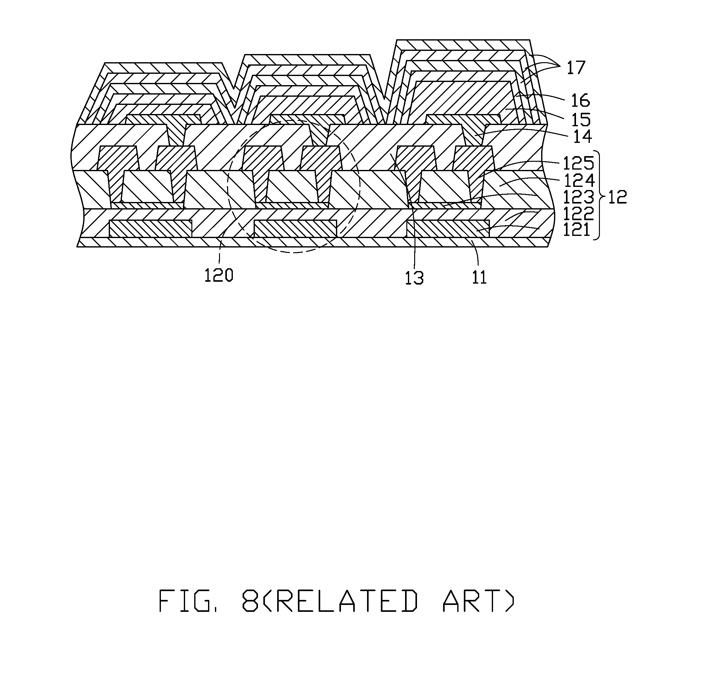
[0002] Display panels display images based on light emitted by a backlight module. As shown in FIG. 8, a conventional display panel can include a substrate 11, an array layer 12 of thin film transistors (TFT) formed on the substrate 11, an insulating layer 13 formed on the TFT array layer 12, a first conducting layer 14 formed on the insulating layer 13, light emitting elements 15 formed on the insulating layer 13, a second conducting layer 16 formed on the light emitting elements 15, and the encapsulating layers 17 formed on the second conducting layer 16. The TFT array layer 12 includes a plurality of TFTs 120 in a matrix. The insulating layer 13 is positioned between the TFT array layer 12 and the plurality of light emitting elements 15. The insulating layer 13 covers the plurality of TFTs 120, and insulates the plurality of TFTs 120 from the plurality of light emitting elements 15. The encapsulating layers 17 encapsulate the light emitting elements 15. The light emitting elements 15 may be organic light emitting diodes (OLEDs), micro-light emitting diodes (pLEDs), or quantum dots light emitting diodes (QLED). A micro-light emitting diode may be 50.times.50 .mu.m in size. A top surface of the conducting layer 14 close to the light emitting elements 15 is substantially flat. However, the light emitting elements 15 of different colors formed on the top surface 131 of the insulating layer 13 have different sizes, and especially have different heights. Different sizes of different color light emitting elements 15 cause wrinkles in display panel and packaging surfaces of the encapsulating layers 17 are not flat when the light emitting elements 15 are encapsulated by a thin film encapsulation technology. This leads to holes or apertures in the encapsulating layers 17, and moisture may enter the display panel from these holes or apertures. The light emitting elements 15 are .mu.LEDs. Fabrication of the display panel comprises transferring the .mu.LEDs onto the top surface 131 of the insulating layer 13 so as to transfer .mu.LEDs of one color at one time. .mu.LEDs with different colors have different heights, .mu.LEDs of one color having a specified height. The blue .mu.LEDs may be transferred last. During the transfer of the blue .mu.LEDs, the blue .mu.LEDs to face the already-mounted red or green .mu.LEDs are connected to the red or green .mu.LEDs based on the different heights of the .mu.LEDs, the blue .mu.LEDs being assembled in the wrong positions, effectively speaking.
[0003] Thus, there is room for improvement in the art.
BRIEF DESCRIPTION OF THE FIGURES
[0004] Implementations of the present technology will now be described, by way of example only, with reference to the attached figures.
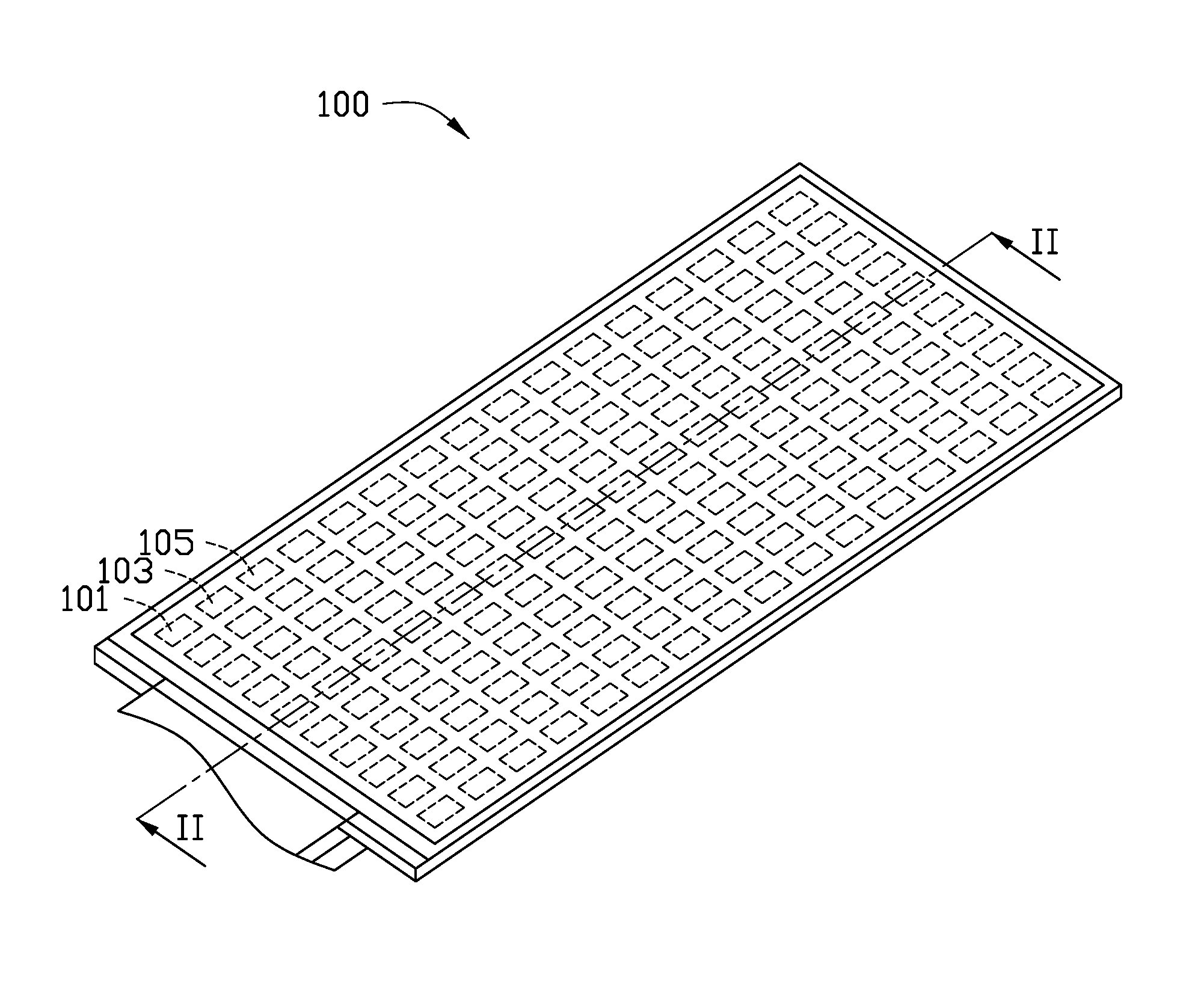
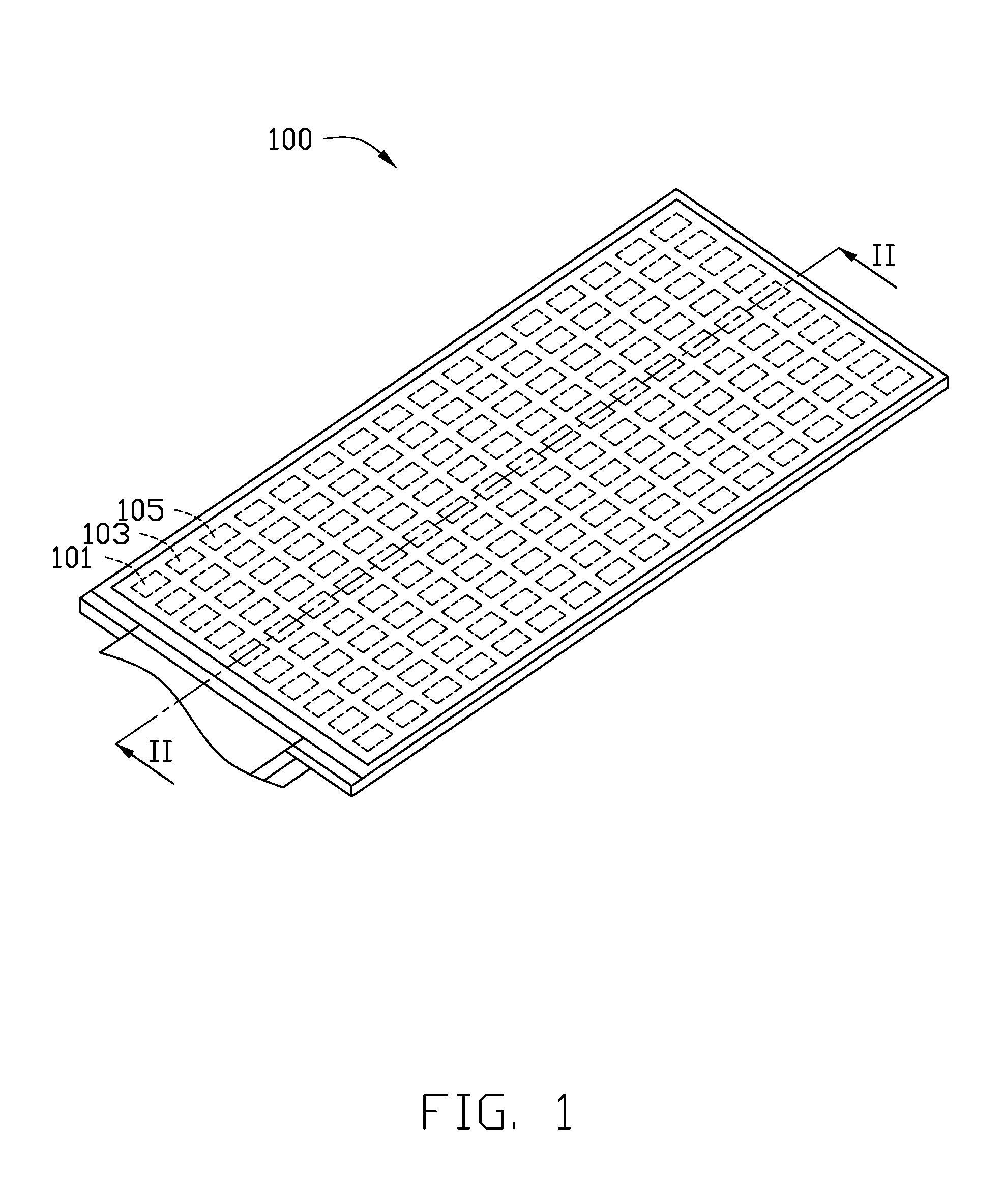
[0005] FIG. 1 is an isometric view of an embodiment of a display panel.
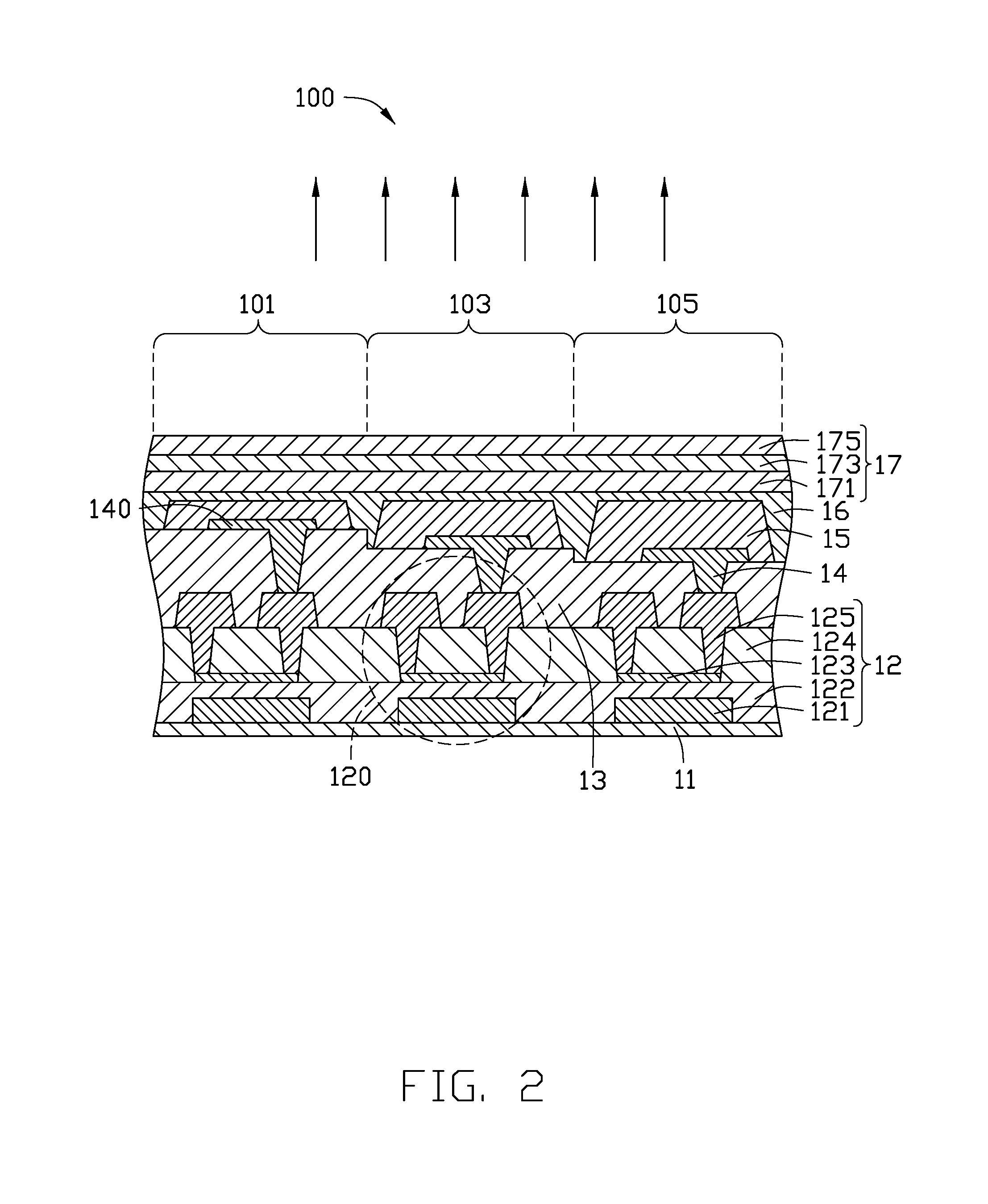
[0006] FIG. 2 is a cross-sectional view of a first embodiment of the display panel of FIG. 1.
[0007] FIG. 3 is a flowchart of a first embodiment of a method for fabricating the display panel of FIG. 2.
[0008] FIGS. 4A-4E are cross-sectional views of structure development in steps 41 through 44 of the method of FIG. 3.
[0009] FIG. 5 is a cross-sectional view of a second embodiment of the display panel of FIG. 1.
[0010] FIG. 6 is a flowchart of a second embodiment of a method for fabricating the display panel of FIG. 5.
[0011] FIGS. 7A-7F are cross-sectional views of structure development in steps 61 through 65 of the method of FIG. 6.
[0012] FIG. 8 is a cross-sectional view of a display panel in a related art.
DETAILED DESCRIPTION
[0013] It will be appreciated that for simplicity and clarity of illustration, where appropriate, reference numerals have been repeated among the different figures to indicate corresponding or analogous elements. In addition, numerous specific details are set forth in order to provide a thorough understanding of the embodiments described herein. However, it will be understood by those of ordinary skill in the art that the embodiments described herein can be practiced without these specific details. In other instances, methods, procedures, and components have not been described in detail so as not to obscure the related relevant feature being described. The drawings are not necessarily to scale and the proportions of certain parts may be exaggerated to better illustrate details and features. The description is not to be considered as limiting the scope of the embodiments described herein.
[0014] The term "comprising" means "including, but not necessarily limited to"; it specifically indicates open-ended inclusion or membership in a so-described combination, group, series, and the like. The disclosure is illustrated by way of example and not by way of limitation in the figures of the accompanying drawings in which like references indicate similar elements. It should be noted that references to "an" or "one" embodiment in this disclosure are not necessarily to the same embodiment, and such references can mean "at least one."
[0015] The present disclosure provides a display panel with the light emitting elements arranged so as to be present a substantially flat top surface. Top surfaces of the light emitting elements of all color are in one plane.
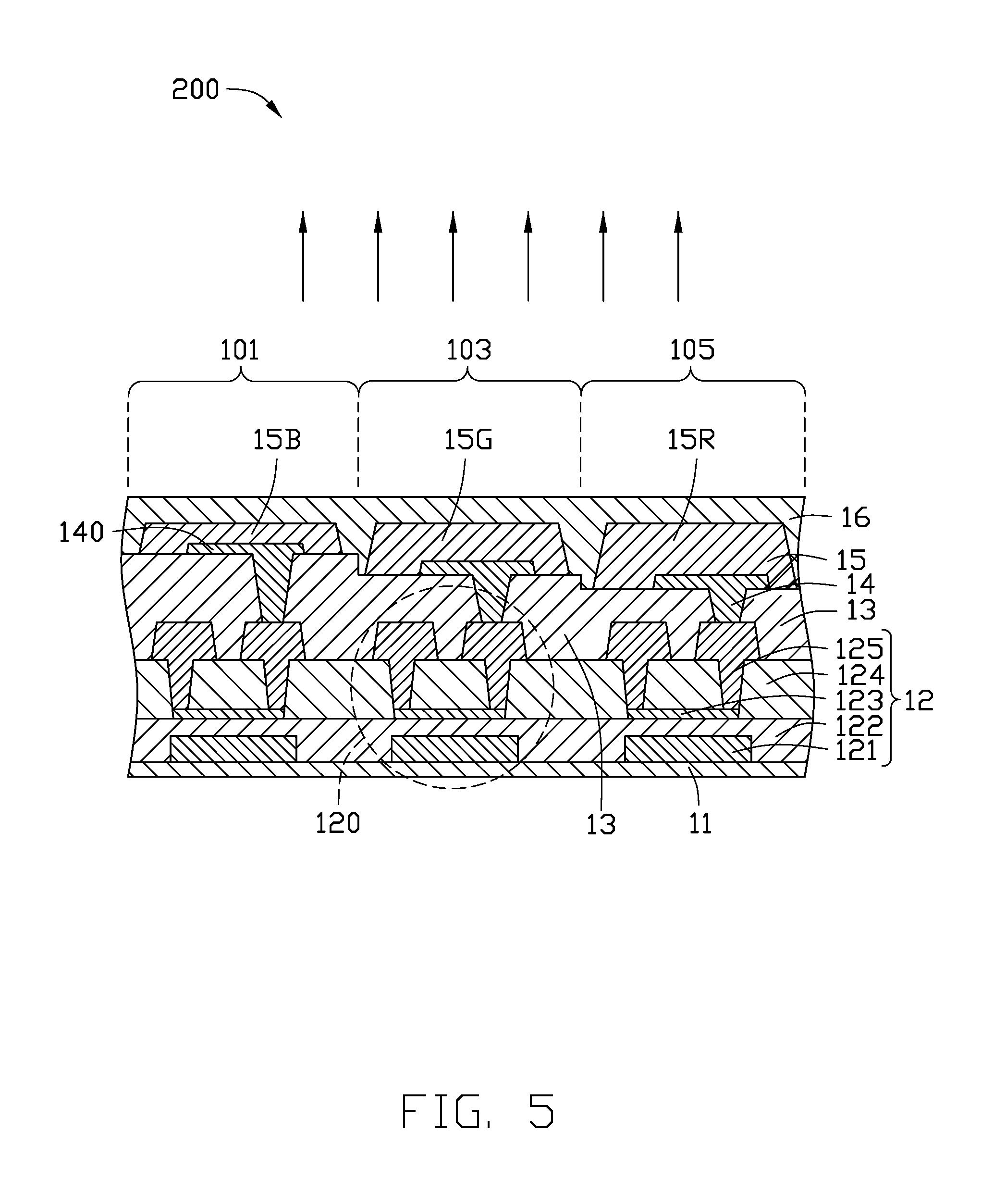
[0016] FIGS. 1 and 2 show a display panel 100 according to a first embodiment. The display panel 100 defines first panel regions 101, second panel regions 103, and third panel regions 105. Each first panel region 101, each second panel region 103, and each third panel region 105 corresponds to a sub-pixel. Each second region 103 is disposed between one of the first panel regions 101 and one of the third panel regions 105. In the embodiment, each first panel region 101 represents a blue sub-pixel, each second panel region 103 a green sub-pixel represents a green sub-pixel, and each third panel region 105 represents a red sub-pixel. In other embodiments, the display panel 100 further can defines fourth regions serving as white sub-pixels. FIG. 2 only shows one first panel region 101, one second panel region 103, and one third panel region 105.
[0017] The display panel 100 includes a substrate 11, a TFT array layer 12, an insulating layer 13, a first conducting layer 14, a light emitting layer 15 with light emitting elements, a second conducting layer 16, and at least one encapsulating layer 17.
[0018] The substrate 11 provides structural support. The substrate 11 typically includes an insulating material. Suitable materials for the substrate 11 may include glass, quartz, and plastic, which has sufficient optical transparency. In some embodiments, the substrate 11 may comprise ceramic and/or silicon materials. In some applications, flexible substrate materials may be adopted. Suitable choices of material for the flexible substrate may include, for example, polyethersulfone (PES), polyethylenenaphthalate (PEN), polyethylene (PE), polyimide (PI), polyvinyl chloride (PVC), and polyethylene terephthalate (PET), or combinations thereof.
[0019] The TFT array layer 12 is arranged on a surface of the substrate 11. The TFT array layer 12 includes TFTs 120 in a matrix. The TFT array layer 12 includes a gate layer 121, a gate insulating layer 122, a channel layer 123, a barrier layer 124, and a source/drain layer 125. The gate layer 121 is located on a surface of the substrate 11, and is patterned to form gate electrodes of the TFTs 120. The gate insulating layer 122 is located on a surface of the gate layer 121 away from the substrate 11. The gate insulating layer 122 insulates the gate layer 121 from the channel layer 123. The channel layer 123 is located on a surface of the gate insulating layer 122 away from the gate layer 121. The channel layer 123 is patterned to form channels of the TFTs 120. The barrier layer 124 is located on a surface of the channel layer 123 away from the gate insulating layer 122. The barrier layer 124 provides insulation between the channel layer 122 and the source/drain layer 125. The source/drain layer 125 is located on a surface of the channel layer 123 away from the gate insulating layer 122. The source/drain layer 125 is patterned to form source and drain electrodes of the TFTs 120. The source and drain electrodes of the TFTs 120 are electrically connected to the channel layer by passing through the barrier layer 124. In the embodiment, the TFT 120 is a bottom type TFT. In other embodiments, the gate layer 121 can be arranged on the source/drain layer 125 to form a top type TFT 120.
[0020] The insulating layer 13 is arranged on a surface of the TFT array layer 12 away from the substrate 11. Thicknesses of the insulating layer 13 corresponding to the first, second, and third panel regions 101, 103, and 105 are different from each other along the light emitting direction. A thickness of the insulating layer 13 corresponding to the first panel regions 101 is thicker than a thickness of the insulating layer 13 corresponding to the second panel regions 103. The thickness of the insulating layer 13 corresponding to the second panel regions 103 is thicker than a thickness of the insulating layer 13 corresponding to the third panel regions 105.
[0021] The first conducting layer 14 is arranged on a surface of the insulating layer 13 away from the TFT array layer 12. The first conducting layer 14 is patterned to form first electrodes 140. The first electrodes 140 are electrically connected with the source/drain layer 125 passing through the insulating layer 13. Each first electrode 140 is an anode of the light emitting elements. In another embodiment, each first electrode 140 can be a cathode of the light emitting elements of the light emitting layer 15.
[0022] The light emitting layer 15 is arranged on a surface of the insulating layer 13 away from the TFT array layer 12. The light emitting layer 15 further covers side surfaces and top surfaces of a corresponding first electrode 140, and encapsulates the corresponding first electrode 140. A top surface of the light emitting layer 15 is substantially flat. The light emitting layer 15 includes first light emitting elements 15B, second light emitting elements 15G, and third light emitting elements 15R. In the embodiment, each first light emitting element 15B, each second light emitting element 15G, and each third light emitting element 15R is an organic light emitting diode (OLED). Each first light emitting element 15B, second light emitting element 15G, and third light emitting element 15R corresponds to one TFT 120. Each first light emitting element 15B emits first color light, e.g., blue, and faces each first panel region 101. Each second light emitting element 15G emits second color light, e.g., green, and faces each second panel region 103. Each third light emitting element 15R emits third color light, e.g., red, and faces each third panel region 105. In other embodiments, the light emitting layer 15 can also include fourth emitting elements emitting white light, each fourth emitting element corresponding to a fourth region. Each first light emitting element 15B is in a first specified thickness, each second light emitting element 15G, is in a second specified thickness, and each third light emitting element 15R is in a third specified thickness. The first specified thickness is thinner than the second specified thickness, and the second specified thickness is thinner than the third specified thickness. Top surfaces of the first, second, and third light emitting elements 15B, 15G, and 15R away from the insulating layer 13 are coplanar.
[0023] The second conducting layer 16 is arranged on a surface of the light emitting layer 15 away from the insulating layer 13, and fills in the gaps between the light emitting elements 12B, 15G, and 15R. The second conducting layer 16 is a cathode of the light emitting elements of the light emitting layer 15. In other embodiments, the second conducting layer 16 can be an anode of the light emitting elements of the light emitting layer 15. A top surface of the second conducting layer 16 away from the light emitting layer 15 is substantially flat. The second conducting layer 16 covers side surfaces and top surfaces of a corresponding light emitting element 15.
[0024] The encapsulating layer 17 is arranged on the second conducting layer 15. The encapsulating layer 17 encapsulates the second conducting layer 16 and the light emitting elements 15. A bottom surface of the encapsulating layer 17 adjacent to the second conducting layer 16 and a top surface of the encapsulating layer 17 away from the second conducting layer 16 are flat surfaces. The encapsulating layer 17 can include a first sub-encapsulating layer 171, a second sub-encapsulating layer 173, and a third sub-encapsulating layer 175. The multiple sub-encapsulating layers reinforce each other and enhance the encapsulation.
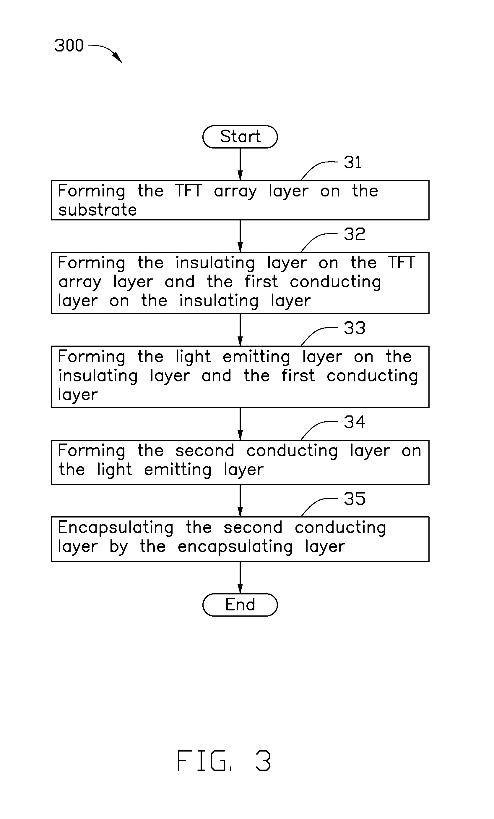
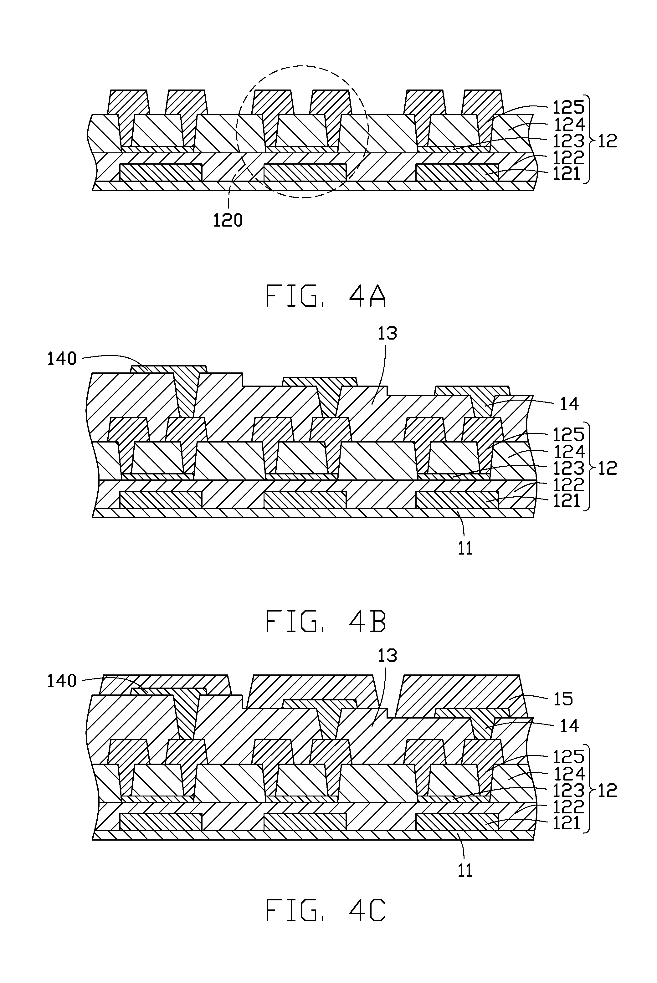
[0025] FIG. 3 shows a method 300 for fabricating the display panel according to a first embodiment. The method 300 is provided by way of example, as there are a variety of ways to carry out the method 300. The method 300 described below may be carried out using the configurations shown in FIGS. 1-2 and FIG. 4A-4D, for example, and various elements of these figures are referenced in explaining the method 300. Each block shown in FIG. 3 represents one or more processes, methods, or subroutines, carried out in the method 300. Furthermore, the order of blocks is illustrative only and the order of the blocks can change. Additional blocks can be added or blocks can be removed, without departing from this disclosure. The method 300 can begin at block 31.
[0026] At block 31, referring also to FIG. 4A, forming a TFT array layer on a substrate 11. The substrate 11 provides structural support. The substrate 11 typically includes an insulating material. Suitable materials for the substrate 11 may include glass, quartz, and plastic, which has sufficient optical transparency. In some embodiments, the substrate 11 may comprise ceramic and/or silicon materials. In some applications, flexible substrate materials may be adopted. Suitable choices of material for the flexible substrate may include, for example, polyethersulfone (PES), polyethylenenaphthalate (PEN), polyethylene (PE), polyimide (PI), polyvinyl chloride (PVC), and polyethylene terephthalate (PET), or combinations thereof. The TFT array layer 12 is arranged on a surface of the substrate 11. The TFT array layer 12 includes TFTs 120 in a matrix. The TFT array layer 12 includes a gate layer 121, a gate insulating layer 122, a channel layer 123, a barrier layer 124, and a source/drain layer 125. The gate layer 121 is located on a surface of the substrate 11, and is patterned to form gate electrodes of the TFTs 120. The gate insulating layer 122 is located on a surface of the gate layer 121 away from the substrate 11. The gate insulating layer 122 insulates the gate layer 121 from the channel layer 123. The channel layer 123 is located on a surface of the gate insulating layer 122 away from the gate layer 121. The channel layer 123 is patterned to form channels of the TFTs 120. The barrier layer 124 is located on a surface of the channel layer 123 away from the gate insulating layer 122. The barrier layer 124 insulates the channel layer 122 and the source/drain layer 125. The source/drain layer 125 is located on a surface of the channel layer 123 away from the gate insulating layer 122. The source/drain layer 125 is patterned to form source and drain electrodes of the TFTs 120.
[0027] At block 32, in FIG. 4B, the insulating layer 13 is formed on the TFT array layer 12 and the first conducting layer 14 is formed on the insulating layer 13. The insulating layer 13 is arranged on a surface of the TFT array layer 12 away from the substrate 11. Thicknesses of the insulating layer 13 corresponding to the first, second, and third panel regions 101, 103, and 105 are different from each other along the light emitting direction. A thickness of the insulating layer 13 corresponding to the first panel regions 101 is thicker than a thickness of the insulating layer 13 corresponding to the second panel regions 103, and the thickness of the insulating layer 13 corresponding to the second panel regions 103 is thicker than a thickness of the insulating layer 13 corresponding to the third panel regions 105. The first conducting layer 14 is arranged on a surface of the insulating layer 13 away from the TFT array layer 12. The first conducting layer 14 is patterned to form first electrodes 140. The first electrodes 140 are electrically connected with the source/drain layer 125 passing through the insulating layer 13. Each first electrode 140 is an anode of the light emitting elements. In other embodiment, each first electrode 140 can be a cathode of the light emitting elements of the light emitting layer 15.
[0028] At block 33, in FIG. 4C, the light emitting layer 15 is formed on the insulating layer 13 and the first conducting layer 14. The light emitting layer 15 is arranged on a surface of the insulating layer 13 away from the TFT array layer 12. The light emitting layer 15 further covers side surfaces and top surfaces of a corresponding first electrode 140, and encapsulates the first electrodes 140. A top surface of the light emitting layer 15 is substantially flat. The light emitting layer 15 includes first light emitting elements 15B, second light emitting elements 15G, and third light emitting elements 15R. In the embodiment, each first light emitting elements 15B, second light emitting elements 15G, and third light emitting elements 15R is an organic light emitting diode (OLED). Each first light emitting element 15B, second light emitting element 15G, and third light emitting element 15R corresponds to one TFT 120. Each first light emitting element 15B, second light emitting element 15G, and third light emitting element 15R corresponds to one TFT 120. Each first light emitting element 15B emits first color light, e.g., blue, and faces each first panel region 101. Each second light emitting element 15G emits second color light, e.g., green, and faces each second panel region 103. Each third light emitting element 15R emits third color light, e.g., red, and faces each third panel region 105. In other embodiments, the light emitting layer 15 can also include fourth emitting elements emitting white light. Each first light emitting element 15B is in a first specified thickness, each second light emitting element 15G is in a second specified thickness, and each third light emitting element 15R is in a third specified thickness. The first specified thickness is thinner than the second specified thickness, and the second specified thickness is thinner than the third specified thickness. Top surfaces of the first, second, third light emitting elements 15B, 15G, and 15R away from the insulating layer 13 are coplanar. The first, second, and third light emitting elements 15B, 15G, 15R are fabricated in an evaporation process.
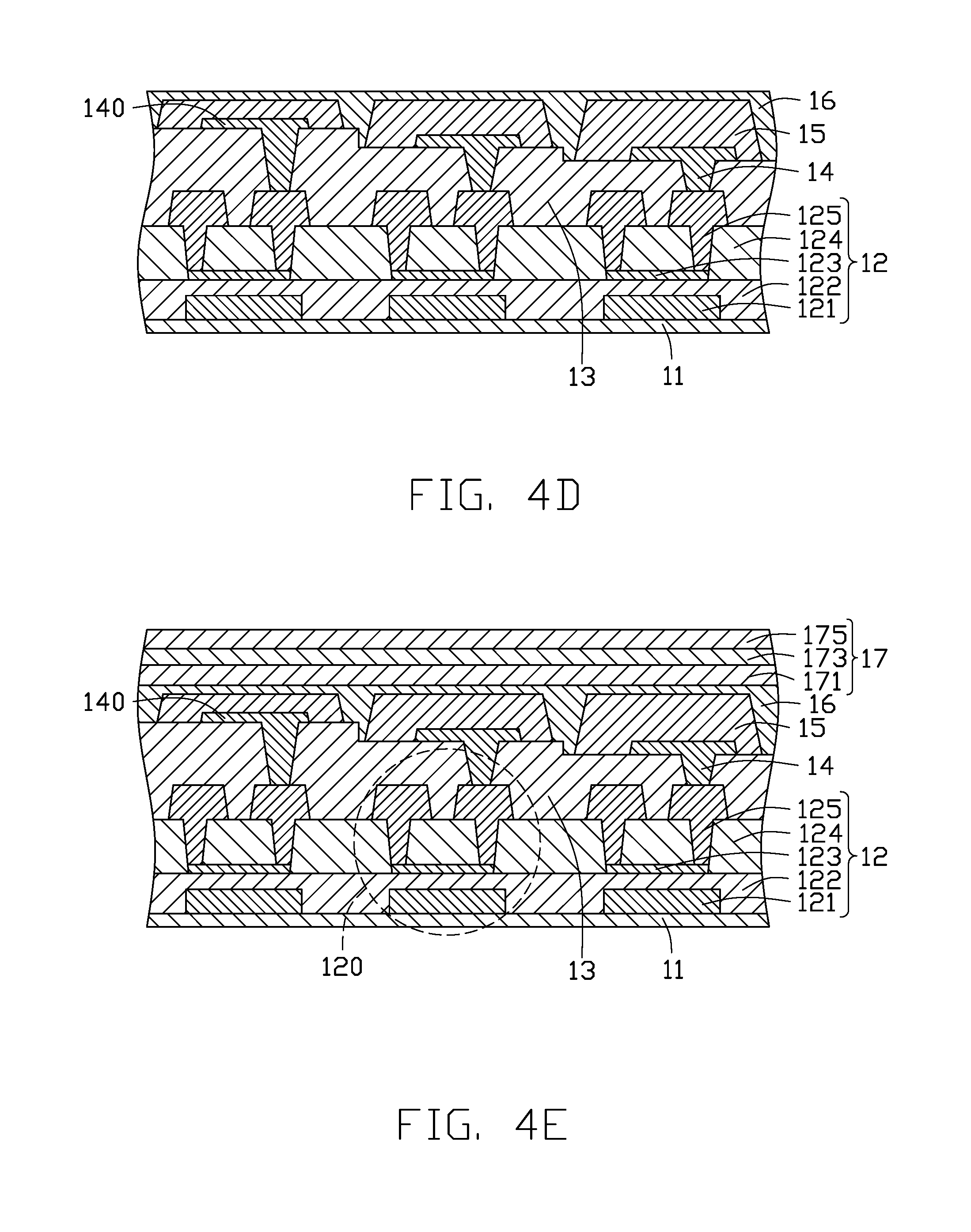
[0029] At block 34, in FIG. 4D, a second conducting layer 16 is formed on the light emitting layer 15. The second conducting layer 16 is arranged on a surface of the light emitting layer 15 away from the insulating layer 13, and fills in the gaps between the light emitting elements 12B, 15G, 15R. The second conducting layer 16 is a cathode of the light emitting elements of the light emitting layer 15. In other embodiments, the second conducting layer 16 can be an anode of the light emitting elements of the light emitting layer 15. A top surface of the second conducting layer 16 away from the light emitting layer 15 is substantially flat.
[0030] At block 35, in FIG. 4E, the second conducting layer 16 is encapsulated by the encapsulating layer 17. The encapsulating layer 17 is arranged on the second conducting layer 16. A top surface of the encapsulating layer 17 is flat. The encapsulating layer 17 can include a first sub-encapsulating layer 171, a second sub-encapsulating layer 173, and a third sub-encapsulating layer 175.
[0031] As the above description, the top surfaces of the first, second, and third light emitting elements 15B, 15G, and 15R away from the insulating layer 13 are coplanar, undesired holes or apertures are effectively prevented, and entrance paths of water or water vapor are reduced. Thus, a performance of the display panel is improved.
[0032] FIG. 5 shows a display panel 200 according to a second embodiment. In the second embodiment, encapsulating layer 17 is removed. The difference between the display panel 200 and the display panel 100 is the light emitting elements 15, and the manner of fabrication of forming the light emitting layer 15.
[0033] The first, second, and third light emitting elements 15B, 15G, 15R are micro-light emitting diodes (.mu.LEDs).
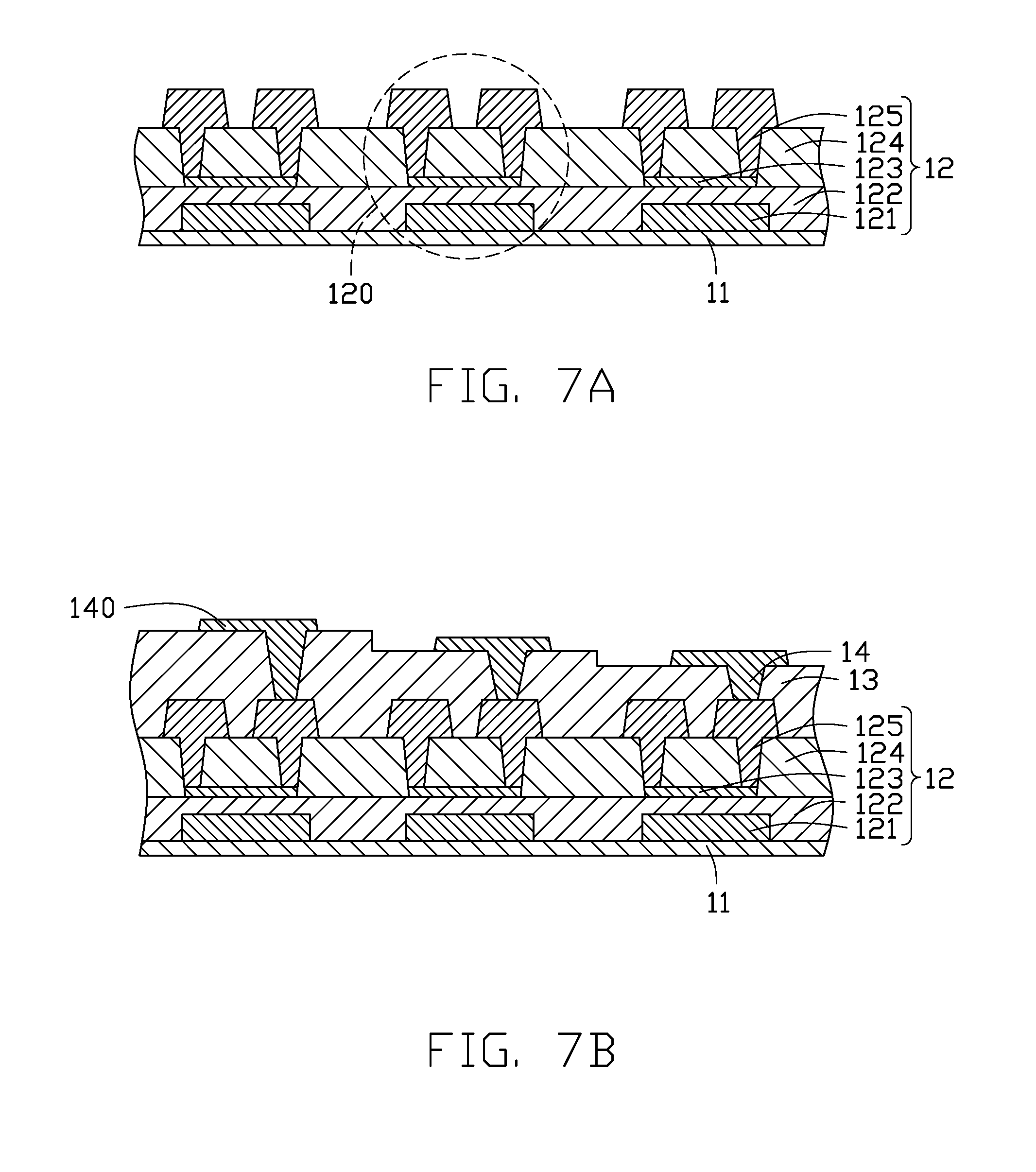
[0034] FIG. 6 shows a method 600 for fabricating the display panel 200 according to a second embodiment. The method 600 is provided by way of example, as there are a variety of ways to carry out the method 600. The method 600 described below may be carried out using the configurations shown in FIG. 5 and FIG. 7A-7F, for example, and various elements of these figures are referenced in explaining the method 600. Each block shown in FIG. 6 represents one or more processes, methods, or subroutines, carried out in the method 600. Furthermore, the order of blocks is illustrative only and the order of the blocks can change. Additional blocks can be added or blocks can be removed, without departing from this disclosure. The method 600 can begin at block 61.
[0035] At block 61, in FIG. 7A, a TFT array layer is formed on a substrate 11. The substrate 11 provides structural support. The substrate 11 typically includes an insulating material. Suitable materials for the substrate 11 may include glass, quartz, and plastic, which has sufficient optical transparency. In some embodiments, the substrate 11 may comprise ceramic and/or silicon materials. In some applications, flexible substrate materials may be adopted. Suitable choices of material for the flexible substrate may include, for example, polyethersulfone (PES), polyethylenenaphthalate (PEN), polyethylene (PE), polyimide (PI), polyvinyl chloride (PVC), and polyethylene terephthalate (PET), or combinations thereof. The TFT array layer 12 is arranged on a surface of the substrate 11. The TFT array layer 12 includes TFTs 120 in a matrix. The TFT array layer 12 includes a gate layer 121, a gate insulating layer 122, a channel layer 123, and a source/drain layer 125. The gate layer 121 is located on a surface of the substrate 11, and is patterned to form gate electrodes of the TFTs 120. The gate insulating layer 122 is located on a surface of the gate layer 121 away from the substrate 11. The gate insulating layer 122 insulates the gate layer 121 from the channel layer 123. The channel layer 123 is located on a surface of the gate insulating layer 122 away from the gate layer 121. The channel layer 123 is patterned to form channels of the TFTs 120. The barrier layer 124 is located on a surface of the channel layer 123 away from the gate insulating layer 122. The barrier layer 124 provides insulation between the channel layer 122 and the source/drain layer 125. The source/drain layer 125 is located on a surface of the channel layer 123 away from the gate insulating layer 122. The source/drain layer 125 is patterned to form source and drain electrodes of the TFTs 120.
[0036] At block 62, referring also to FIG. 7B, forming the insulating layer 13 on the TFT array layer 12 and the first conducting layer 14 on the insulating layer 13. The insulating layer 13 is arranged on a surface of the TFT array layer 12 away from the substrate 11. Thicknesses of the insulating layer 13 corresponding to the first, second, and third panel regions 101, 103, and 105 are different from each other along the light emitting direction. A thickness of the insulating layer 13 corresponding to the first panel regions 101 is thicker than a thickness of the insulating layer 13 corresponding to the second panel regions 103. The thickness of the insulating layer 13 corresponding to the second panel regions 103 is thicker than a thickness of the insulating layer 13 corresponding to the third panel regions 105. The first conducting layer 14 is arranged on a surface of the insulating layer 13 away from the TFT array layer 12. The first conducting layer 14 is patterned to form first electrodes 140. The first electrodes 140 are electrically connected with the source/drain layer 125 passing through the insulating layer 13. Each first electrode 140 is an anode of the light emitting elements. In other embodiment, each first electrode 140 can be a cathode of the light emitting elements of the light emitting layer 15.
[0037] At block 63, in FIG. 7C, the first light emitting elements 15B are transferred on the insulating layer 13 facing the first panel regions 101. The first light emitting elements 15B are arranged on a surface of the insulating layer 13 away from the TFT array layer 12. The first light emitting elements 15B further cover side surfaces and top surfaces of the first electrodes 140, and encapsulate the first electrodes 140. In the embodiment, each first light emitting element 15B is micro-light emitting diode (.mu.LED). Each first light emitting element 15B emits first color light, and faces each first panel region 101. In the embodiment, the first light emitting element 15B emits blue light. Each first light emitting element 15B is in a first specified thickness.
[0038] At block 64, in FIG. 7D, the second light emitting elements 15G are transferred on the insulating layer 13 facing the second panel regions 103. Each second light emitting element 15G emits second color light, and faces each second panel region 103. In the embodiment, the second light emitting element 15G emits green light. Each second light emitting element 15G is in a second specified thickness.
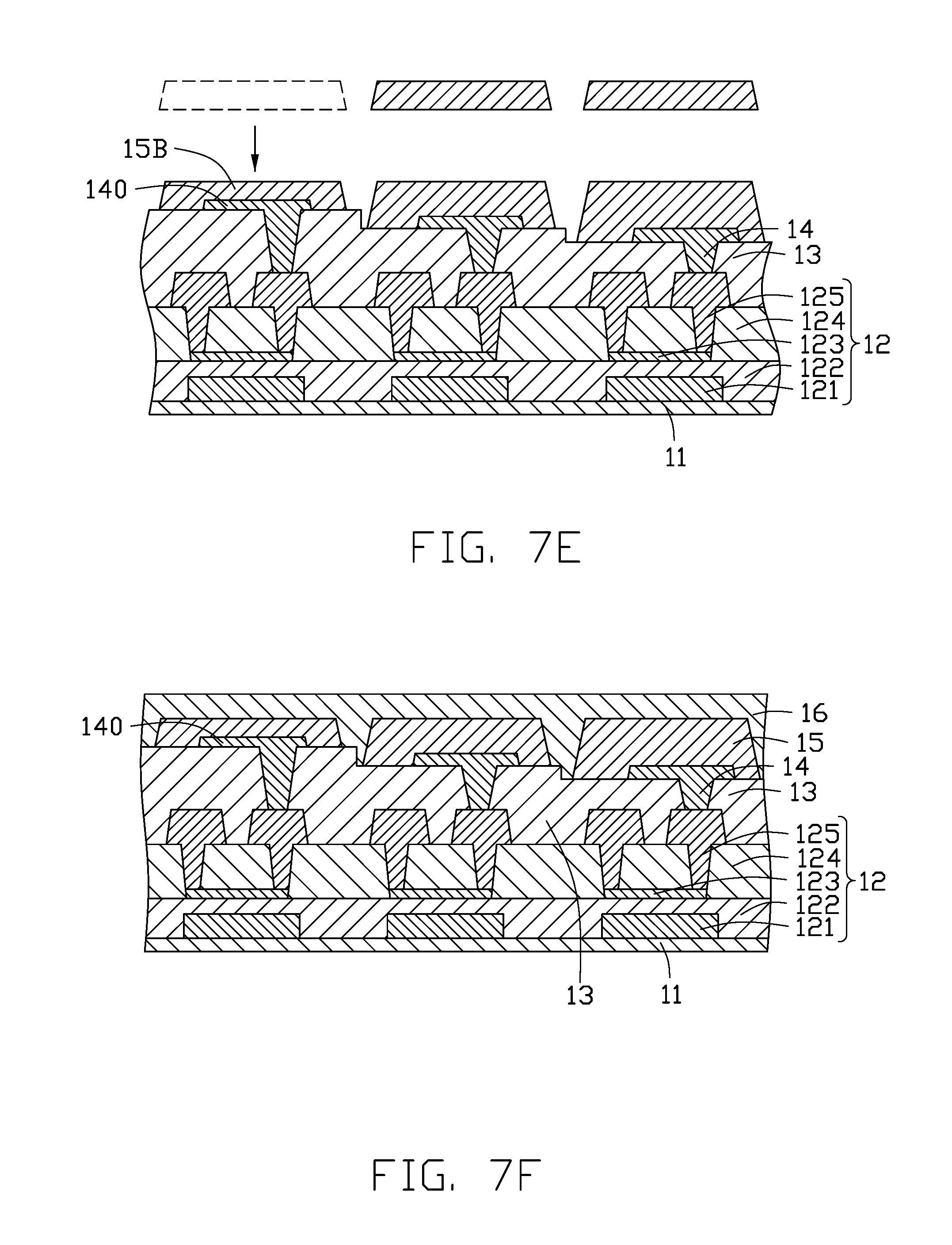
[0039] At block 65, in to FIG. 7E, the third light emitting elements 15R are transferred on the insulating layer 13 facing the third panel regions 105. Each light emitting element 15R emits third color light, and faces each third panel region 105. In the embodiment, the third light emitting element 15R emits red color light. Each third light emitting element 15R is in a third specified thickness. The first specified thickness is thinner than the second specified thickness, and the second specified thickness is thinner than the third specified thickness. Top surfaces of the light emitting layer 15 away from the insulating layer 13 are coplanar.
[0040] At block 66, in FIG. 7F, a second conducting layer 16 is formed on the light emitting layer 15. The second conducting layer 16 is arranged on a surface of the light emitting layer 15 away from the insulating layer 13, and fills in the gaps between the light emitting elements 12B, 15G, and 15R. The second conducting layer 16 is a cathode of the light emitting elements of the light emitting layer 15. In other embodiments, the second conducting layer 16 can be an anode of the light emitting elements of the light emitting layer 15. A top surface of the second conducting layer 16 away from the light emitting layer 15 is substantially flat.
[0041] As the above description, the top surfaces of the light emitting layer 15 away from the insulating layer 13 are coplanar, cross-interference between the transferring operations of the first, second, and third light emitting elements 15B, 15G, and 15R with different color is avoided. Thus, a performance of the display panel is improved.
[0042] While various and preferred embodiments have been described the disclosure is not limited thereto. On the contrary, various modifications and similar arrangements (as would be apparent to those skilled in the art) are also intended to be covered. Therefore, the scope of the appended claims should be accorded the broadest interpretation so as to encompass all such modifications and similar arrangements.
* * * * *
D00000
D00001
D00002
D00003
D00004
D00005
D00006
D00007
D00008
D00009
D00010
D00011
XML
uspto.report is an independent third-party trademark research tool that is not affiliated, endorsed, or sponsored by the United States Patent and Trademark Office (USPTO) or any other governmental organization. The information provided by uspto.report is based on publicly available data at the time of writing and is intended for informational purposes only.
While we strive to provide accurate and up-to-date information, we do not guarantee the accuracy, completeness, reliability, or suitability of the information displayed on this site. The use of this site is at your own risk. Any reliance you place on such information is therefore strictly at your own risk.
All official trademark data, including owner information, should be verified by visiting the official USPTO website at www.uspto.gov. This site is not intended to replace professional legal advice and should not be used as a substitute for consulting with a legal professional who is knowledgeable about trademark law.