Quantum Spin Hall-based Charging Energy-protected Quantum Computation
Pikulin; Dmitry I.
U.S. patent application number 16/195579 was filed with the patent office on 2019-07-18 for quantum spin hall-based charging energy-protected quantum computation. This patent application is currently assigned to Microsoft Technology Licensing, LLC. The applicant listed for this patent is Microsoft Technology Licensing, LLC. Invention is credited to Dmitry I. Pikulin.
| Application Number | 20190220769 16/195579 |
| Document ID | / |
| Family ID | 64650542 |
| Filed Date | 2019-07-18 |
| United States Patent Application | 20190220769 |
| Kind Code | A1 |
| Pikulin; Dmitry I. | July 18, 2019 |
QUANTUM SPIN HALL-BASED CHARGING ENERGY-PROTECTED QUANTUM COMPUTATION
Abstract
This application concerns quantum computing, and in particular to structures and mechanisms for providing topologically protected quantum computation. In certain embodiments, a magnetic tunnel barrier is controlled that separates Majorona zero modes ("MZMs") from an edge area (e.g., a gapless edge) of a quantum spin hall system. In particular implementations, the magnetic tunnel barrier is formed from a pair of magnetic insulators whose magnetization is held constant, and the magnetic tunnel barrier is tuned by controlling a gate controlling the electron density around the magnetic insulator in the QSH plane, thereby forming a quantum dot. And, in some implementations, a state of the quantum dot is read out (e.g., using a charge sensor as disclosed herein).
| Inventors: | Pikulin; Dmitry I.; (Goleta, CA) | ||||||||||
| Applicant: |
|
||||||||||
|---|---|---|---|---|---|---|---|---|---|---|---|
| Assignee: | Microsoft Technology Licensing,
LLC Redmond WA |
||||||||||
| Family ID: | 64650542 | ||||||||||
| Appl. No.: | 16/195579 | ||||||||||
| Filed: | November 19, 2018 |
Related U.S. Patent Documents
| Application Number | Filing Date | Patent Number | ||
|---|---|---|---|---|
| 62588424 | Nov 19, 2017 | |||
| Current U.S. Class: | 1/1 |
| Current CPC Class: | H01L 43/065 20130101; H01L 43/04 20130101; H01L 49/003 20130101; G06N 10/00 20190101; H01L 49/006 20130101 |
| International Class: | G06N 10/00 20060101 G06N010/00; H01L 43/06 20060101 H01L043/06; H01L 43/04 20060101 H01L043/04; H01L 49/00 20060101 H01L049/00 |
Claims
1. A method of operating quantum device comprising: controlling a magnetic tunnel barrier that separates Majorona zero modes ("MZMs") from a gapless edge of a quantum spin hall system, wherein the magnetic tunnel barrier is formed from a magnetic insulator whose magnetization is held constant, and wherein the magnetic tunnel barrier is tuned by controlling a gate controlling the electron density around the magnetic insulator in the QSH plane, thereby forming a quantum dot.
2. The method of claim 1, further comprising reading out a state of the quantum dot.
3. The method of claim 1, wherein the quantum spin hall system implements a tetron qubit.
4. The method of claim 3, wherein the tetron qubit does not comprise a Josephson junction.
5. The method of claim 3, wherein the tunable quantum dot is further located between or substantially between two magnetic insulators.
6. The method of claim 5, wherein the two magnetic insulators are non-tunable.
7. The method of claim 1, wherein the quantum spin hall system implements a hexon qubit.
8. The method of claim 7, wherein the tetron qubit does not comprise a Josephson junction.
9. The method of claim 7, wherein the tunable quantum dot is further located between or substantially between two magnetic insulators.
10. The method of claim 7, wherein the two magnetic insulators are non-tunable.
11. A tetron qubit, comprising three pairs of Majorana zero modes, wherein the tetron qubit further comprises a tunable quantum dot configured to control a magnetic tunnel barrier between two neighboring Majorana zero modes.
12. The tetron qubit of claim 11, wherein the tetron qubit does not comprise a Josephson junction.
13. The tetron qubit of claim 11, wherein the tunable quantum dot is further located between or substantially between two magnetic insulators.
14. The tetron qubit of claim 13, wherein the two magnetic insulators are non-tunable.
15. The tetron qubit of claim 11, wherein the tetron qubit is part of a topologically protected quantum computing system.
16. A hexon qubit comprising four pairs of Majorana zero modes, wherein the hexon qubit further comprises a tunable quantum dot configured to control a magnetic tunnel barrier between two neighboring Majorana zero modes.
17. The hexon qubit of claim 16, wherein the hexon qubit does not comprise a Josephson junction.
18. The hexon qubit of claim 16, wherein the tunable quantum dot is further located between or substantially between two magnetic insulators.
19. The hexon qubit of claim 18, wherein the two magnetic insulators are non-tunable.
20. The hexon qubit of claim 16, wherein the hexon qubit is part of a topologically protected quantum computing system.
Description
CROSS-REFERENCE TO RELATED APPLICATIONS
[0001] This application claims the benefit of U.S. Provisional Application No. 62/588,424 entitled "QUANTUM SPIN HALL-BASED CHARGING ENERGY-PROTECTED QUANTUM COMPUTATION" and filed on Nov. 19, 2017, which is hereby incorporated herein by reference.
FIELD
[0002] This application concerns quantum computing, and in particular to structures and mechanisms for providing topologically protected quantum computation.
BACKGROUND
[0003] Quantum spin Hall ("QSH") systems provide a natural pathway towards the realization of Majorana zero modes ("MZMs") in a condensed matter system, and are a viable platform for the realization of topological quantum computation. Proposals to have topological quantum computation in QSH systems so far (see, e.g., S. Mi et al., Phys. Rev. B 87, 241405(R) (2013)) suffer from: (a) limited scalability due to the ld structure of the QSH edge; (b) they are not charging-energy-protected; and (c) they require tuning by a magnetic field. Accordingly, improved QSH systems that are scalable, charging-energy-protected and/or free of an external magnetic field are desired.
SUMMARY
[0004] As noted, current approaches for providing topological quantum computation in a QSH system suffer from: (a) limited scalability due to the ld structure of the QSH edge; (b) they are not charging energy-protected; and (c) they require tuning of magnetic field. Embodiments of the disclosed technology address one or more of these issues by providing a patterning of the QSH device in a regular manner, which allows scaling to arbitrary large systems and allows all protected operations. Further, embodiments of the disclosed technology are arranged so that the design can be implemented in a charging energy-protected way. Also disclosed herein are embodiments that provide a new way to connect and disconnect the MZMs necessary to perform the quantum computation in such systems. For example, certain embodiments use QSH systems gated into bulk conduction regions.
[0005] In certain embodiments, a magnetic tunnel barrier is controlled that separates Majorona zero modes ("MZMs") from an edge area (e.g., a gapless edge) of a quantum spin hall system. For example, the magnetic tunnel barrier can be formed by a magnetic insulator whose magnetization is held constant, and such magnetic tunnel barrier can be tuned by controlling a gate in the area of the magnetic insulator. Two of such tunnel barriers can form a quantum dot located between them. The state of the quantum dot can be read out (e.g., using a charge sensor). In further implementations, a tetron qubit is formed from the quantum spin Hall system. In some instances, the tetron qubit does not comprise a Josephson junction. The tunable quantum dot can be located between or substantially between two magnetic insulators. In certain implementations, the two magnetic insulators are non-tunable. In other embodiments, a hexon qubit is formed from the quantum spin Hall system. In some instances, the hexon qubit does not comprise a Josephson junction. The tunable quantum dot can be located between or substantially between two magnetic insulators. Further, in certain implementations, the two magnetic insulators are non-tunable.
[0006] Further embodiments of the disclosed technology include a tetron qubit with an extra island containing a pair of Majorana zero modes. Such a qubit comprises three pairs of Majorana zero modes, where the qubit further comprises tunable quantum dots configured to control a magnetic tunnel barrier between two neighboring Majorana zero modes. In some embodiments, the tetron qubit does not comprise a Josephson junction. In certain embodiments, the tunable quantum dots are further located between or substantially between two magnetic insulators (e.g., in some implementations, the two magnetic insulators are non-tunable). In further embodiments, the tetron qubit is part of a topologically protected quantum computing system.
[0007] Other embodiments of the disclosed technology include a hexon qubit and a coherent link comprising four pairs of Majorana zero modes, wherein the hexon qubit further comprises a tunable quantum dots configured to control a magnetic tunnel barrier between two neighboring Majorana zero modes. In some embodiments, the hexon qubit does not comprise a Josephson junction. In certain embodiments, the tunable quantum dot is further located between or substantially between two magnetic insulators (e.g., in some implementations, the two magnetic insulators are non-tunable). In further embodiments, the hexon qubit is part of a topologically protected quantum computing system.
[0008] The foregoing and other objects, features, and advantages of the disclosed technology will become more apparent from the following detailed description, which proceeds with reference to the accompanying figures.
BRIEF DESCRIPTION OF THE DRAWINGS
[0009] The patent or application file contains at least one drawing executed in color. Copies of this patent or patent application publication with color drawing(s) will be provided by the Office upon request and payment of the necessary fee.
[0010] FIG. 1 is a schematic block diagram showing a key to the notation used in FIG. 2-6.
[0011] FIG. 2 is a schematic block diagram illustrating an approach to control a magnetic tunnel barrier.
[0012] FIG. 3 is a schematic block diagram showing a hybrid design for a tetron (e.g., with all possible measurements).
[0013] FIG. 4 is a schematic block diagram showing a top view of a quantum dot measurement-only design for a tetron with all possible measurements.
[0014] FIG. 5 is a schematic block diagram showing a top view of a quantum dot measurement-only design for a hexon with all possible two-MZM measurements.
[0015] FIG. 6 is a schematic block diagram showing a top view of a Quantum dot measurement-only design for a hexon with all possible two-MZM measurements, where the design has been scaled up.
[0016] FIG. 7 is a flow chart illustrating an example embodiment for operating quantum device.
DETAILED DESCRIPTION
I. General Considerations
[0017] The disclosed methods, apparatus, and systems should not be construed as limiting in any way. Instead, the present disclosure is directed toward all novel and nonobvious features and aspects of the various disclosed embodiments, alone or in various combinations and subcombinations with one another. Furthermore, any features or aspects of the disclosed embodiments can be used in various combinations and subcombinations with one another. For example, one or more method acts from one embodiment can be used with one or more method acts from another embodiment and vice versa. The disclosed methods, apparatus, and systems are not limited to any specific aspect or feature or combination thereof, nor do the disclosed embodiments require that any one or more specific advantages be present or problems be solved.
[0018] Various alternatives to the examples described herein are possible. The various aspects of the disclosed technology can be used in combination or separately. Different embodiments use one or more of the described innovations. Some of the innovations described herein address one or more of the problems noted in the background. Typically, a given technique/tool does not solve all such problems.
[0019] As used in this application and in the claims, the singular forms "a," "an," and "the" include the plural forms unless the context clearly dictates otherwise. Additionally, the term "includes" means "comprises." Further, as used herein, the term "and/or" means any one item or combination of any items in the phrase.
II. Example Embodiments of the Disclosed Technology
[0020] In the embodiments below, quantum spin Hall ("QSH") systems are used as examples where the technology can be applied. However, the scope of the technology is not limited to QSH systems. In particular, higher-order topological insulators have states on the hinges similar to the ones the QSH systems have on their edges, hence the edge of the example QSH systems disclosed herein can be replaced with a hinge or atomic step of higher-order topological insulators.
[0021] The disclosed examples of the QSH systems can be fabricated, for example, using WTe.sub.2 monolayers, HgTe/CdTe quantum wells, and/or InAs/GaSb quantum wells. WTe.sub.2 monolayers have the additional property that the superconducting region can be gate-tuned, not fabricated in the sample. Example implementations of the second-order topological insulators comprise Bi.
[0022] Quantum spin Hall ("QSH") based systems promise a route toward topological quantum computation by creating an interface with superconductors and magnetic insulators and localizing Majorana zero modes ("MZMs") between them. Current proposals for the realizations of topological qubits in QSH-based system, however, are not in the charging-energy protected regime and are not based on the measurement-only protocol. Additionally, there are no truly scalable proposals due to the 1-dimensional nature of the QSH edge states, where MZMs can be formed. Further, current proposals rely on controlling the magnetic field (locally or globally).
[0023] Embodiments of the disclosed technology address the problems of the current proposals by using a tunable quantum dot in the QSH bulk to connect the otherwise disconnected QSH edges, and to make an effective two-dimensional structure out of the edge states. One advantage of such an approach is that the edges remain disconnected unless required by the ongoing measurement. This gives exponentially well disconnected MZMs between quantum computing operations. On top of that, compared to other approaches, fewer gates can be used to control each of the quantum dots (e.g., two fewer gates than in a previous four-gate arrangement).
[0024] A further advantage of the disclosed technology is the choice between electric and magnetic control of the tunnel barriers. By aligning the magnetization of the magnet parallel and perpendicular to the spin quantization axis of the QSH edge states, one can control transmission through the barrier. Further embodiments disclosed herein comprise tuning the gate voltage for the local gate near the magnet, thus avoiding the tuning of the magnetic field altogether.
[0025] Certain embodiments of the disclosed technology address the issues of the current proposals by providing a charging energy-protected, measurement-only scalable design for qubits in a QSH system. The qubits can be, for example, Majorana hexon qubits or Majorana tetron qubits. Further, some embodiments use a static magnetic insulator.
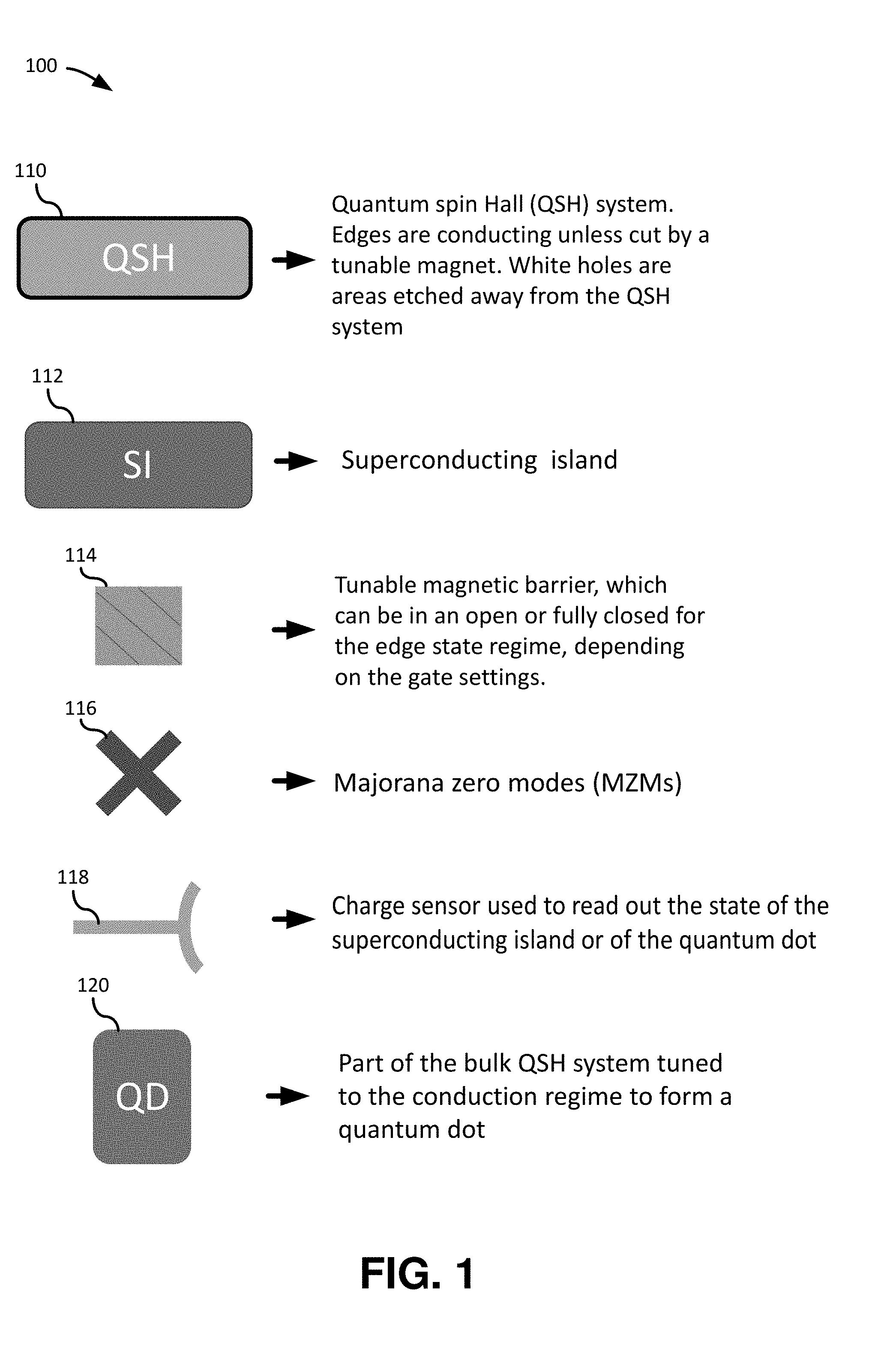
[0026] FIG. 1 is a schematic block diagram 100 showing a key to the notation used in the figures below. In particular, FIG. 1 illustrates the notational scheme used in FIGS. 2-6. As shown at 110, the structural portions shown in green and delineated by "QSH" represent a quantum spin hall system. Further, in the illustrated embodiments, the edges are conducting unless cut by a tunable magnet, and the white holes (shown as rectangular cutouts) are areas etched from the QSH system. As shown at 112, the structural portion shown in blue and delineated by "SI" represent a superconducting island. As shown at 114, the structural portion shown in orange with blue hatches represent a tunable magnetic barrier. The tunable magnetic barrier can be in an open- or fully-closed-for-the-edge-state regime, depending on the gate setting. As shown at 116, the structural portion shown as a red "X" represents a Majorana zero mode ("MZM"), which is also referred to herein as a "Majorana". As shown at 118, the structural portion shown by a semi-circle and a perpendicular branch represents a charge sensor used to read out the state of the superconducting island or of a quantum dot. As shown at 120, the structural portion shown in red and delineated "QD" represents part of the bulk QSH system tuned to the conduction regime to form a quantum dot.
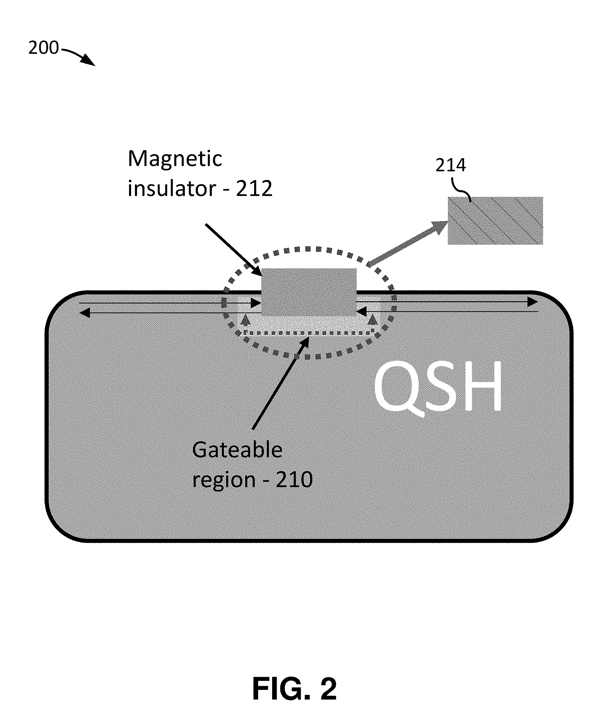
[0027] FIG. 2 is a schematic cross-sectional side view 200 illustrating the control of a magnetic tunnel barrier. In general, two approaches can be used to control a magnetic tunnel barrier separating a MZM from the open areas of a QSH edge. A first example approach comprises controlling the magnetization of the magnet by a local high field coil. A second example approach, and as illustrated in FIG. 2, comprises controlling a local gate (denoted as gate region 210) adjacent to the magnet region (shown by magnetic insulator 212) to tune the system into the bulk QSH bands and allow transmission of electrons through the magnetic region (resulting in a tunable magnetic barrier, as illustrated at 214). This second approach has the advantage of allowing full electrical control of the QSH topological qubit system. Further, the size of the magnet region can be a variety of sizes based on the requirements for the tunnel barrier, but in some cases is approximately 100 nm in size.
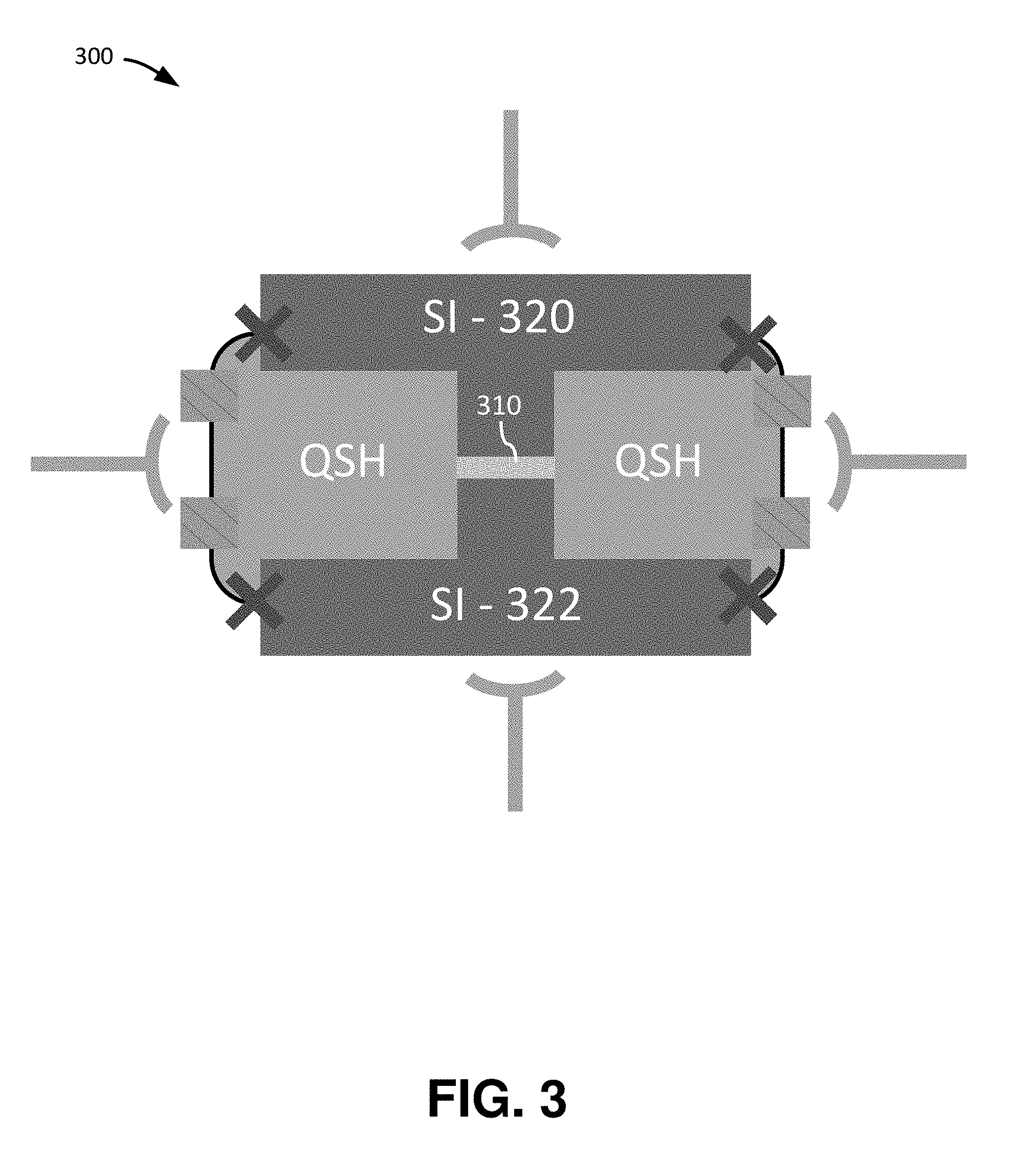
[0028] FIG. 3 is a schematic block diagram 300 showing a top view of a hybrid design for a tetron (e.g., with all possible measurements). The illustrated design relies on a tunable Josephson junction in the middle (shown at 310), which can tune the mutual charging energy of the islands (SI 320 and SI 322) on and off. Unlike in the nanowire case, the absence of an external magnetic field and non-nanowire nature of the junction allows for large tunability of the device. In the figure, measurements are redundant (which is beneficial for testing), but two of the charge sensors can be removed (e.g., one of the top or bottom along with one of the right or left sensors).
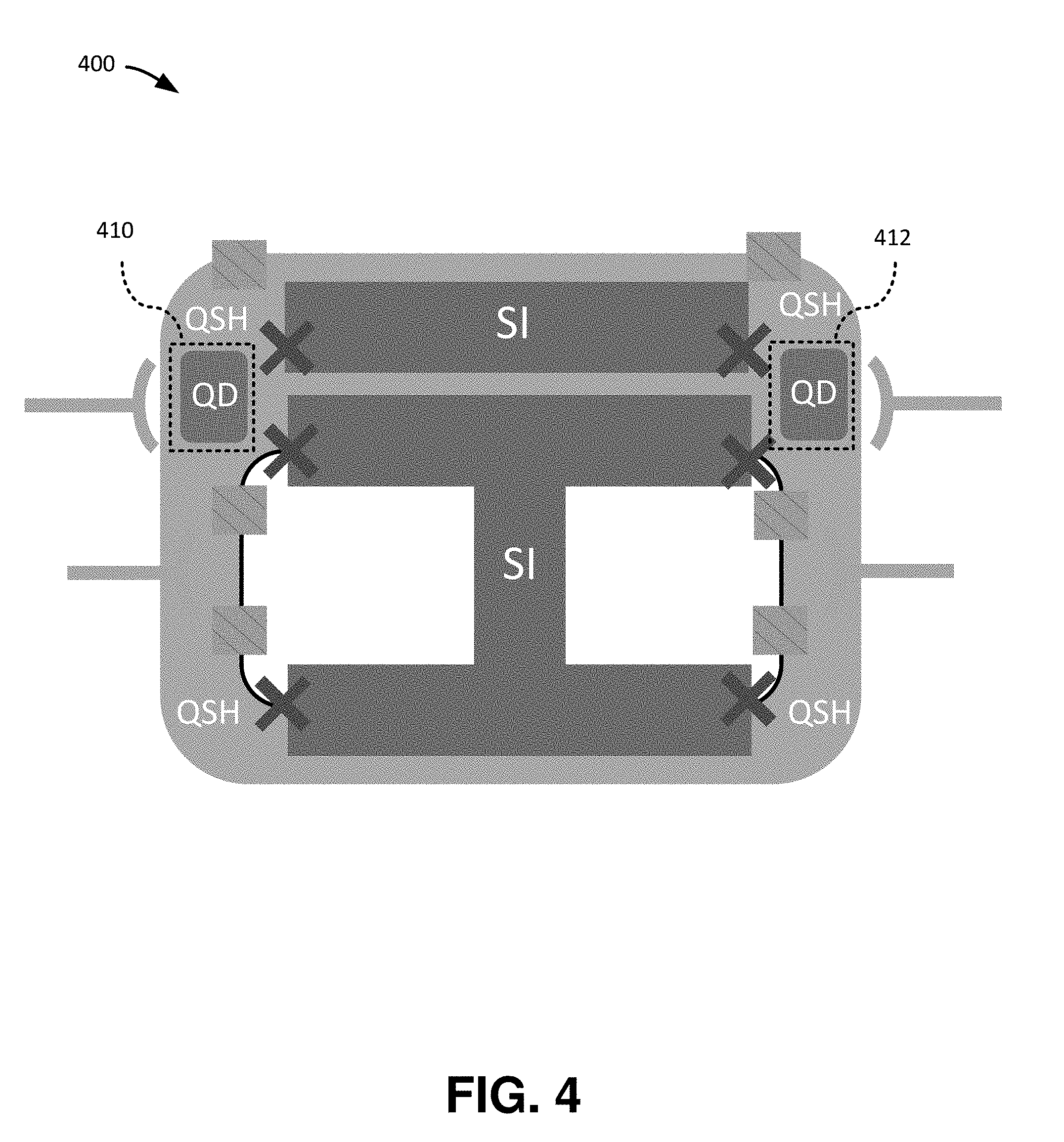
[0029] FIG. 4 is a schematic block diagram 400 showing a top view of a quantum dot measurement-only design for a tetron with all possible measurements. The embodiment illustrated in FIG. 4 has the advantage of not requiring a tunable Josephson junction. Instead, the design adds another element to the design: one or more tunable quantum dots. The quantum dot can be created by a gate from bulk QSH by gating it into the bulk conducting regime (either with positive or negative voltage applied to the gate). In FIG. 4, two quantum dots 410, 412 are illustrated. In some embodiments, the measurement of any one or more of the Majoranas is allowed by opening the respective tunnel barriers and tuning one or more of the quantum dots (e.g., as shown at 410 and 412) into the bulk conducting regime. The size of the quantum dots can vary from implementation to implementation, but in some example implementations is between 180 nm and 220 nm. Further, in some example implementations, the distance between opposing edges of the tunable magnetic barriers is between 30 nm and 70 nm.
[0030] Example designs for Majorana tetron qubits (sometimes referred to as "quad qubits") that can be realized with and/or otherwise incorporate the disclosed technology are described in, for example, Karzig et al., "Scalable Designs for Quasiparticle-Poisoning-Protected Topological Quantum Computation with Majorana Zero Modes," arXiv:1610.05289 (March 2017) and T. Karzig et al., "Scalable Designs for Quasiparticle-Poisoning-Protected Topological Quantum Computation with Majorana Zero Modes," Phys. Rev. B 95, 235305 (2017); U.S. patent application Ser. No. 15/636,457 entitled "QUANTUM COMPUTING METHODS AND DEVICES FOR MAJORANA QUAD QUBITS" and filed on Jun. 28, 2017 (published as U.S. Patent Application Publication No. 2018/0052806), and U.S. Provisional Application No. 62/385,245, entitled "QUANTUM COMPUTING METHODS AND DEVICES FOR MAJORANA QUAD QUBITS" filed on Sep. 8, 2016, all of which are incorporated herein by reference in their entirety.
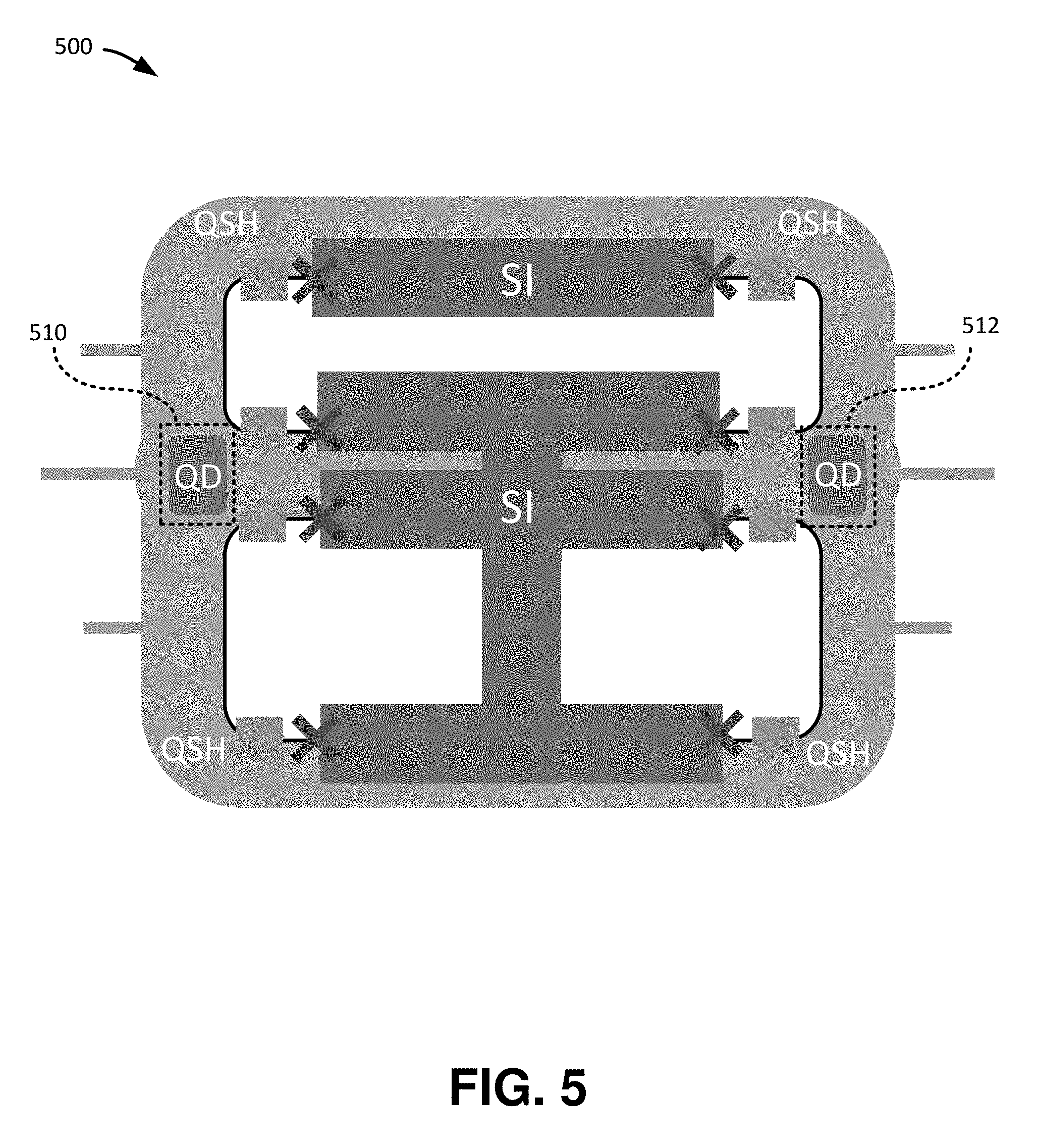
[0031] FIG. 5 is a schematic block diagram 500 showing a top view of a quantum dot measurement-only design for a hexon with all possible two-MZM measurements. This embodiment allows for measurement of any pair of the Majoranas. For instance, in some embodiments, the measurement of any one or more of the Majoranas is allowed by opening the respective tunnel barriers and tuning one or more of the quantum dots (e.g., as shown at 510 and 512) into the bulk conducting regime.
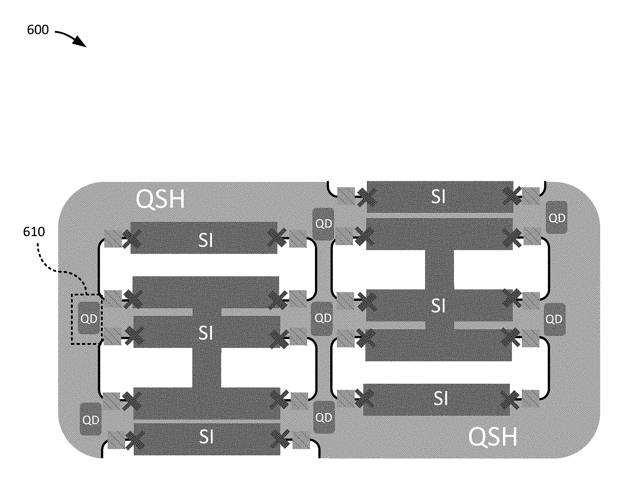
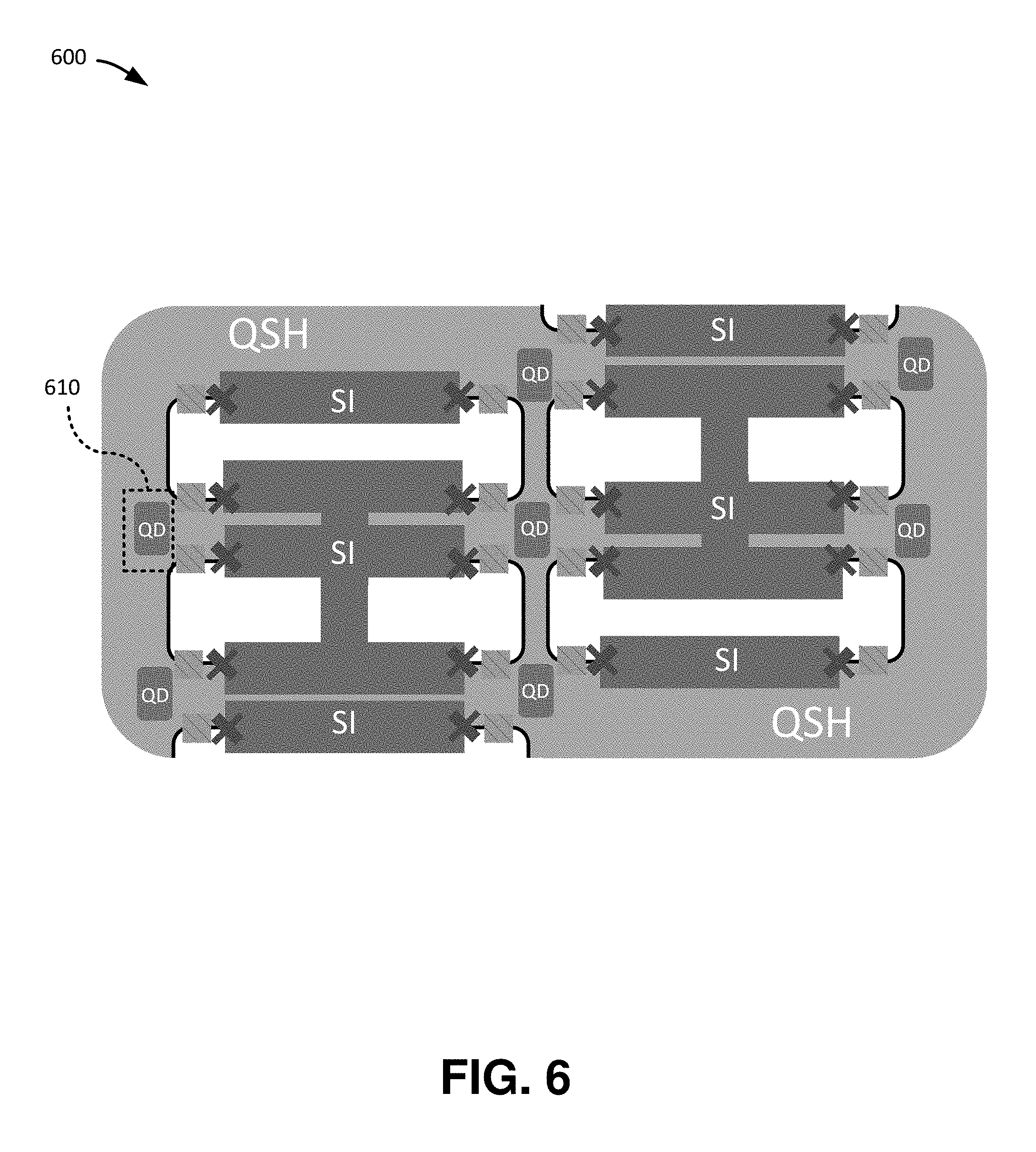
[0032] FIG. 6 is a schematic block diagram 600 showing a top view of a Quantum dot measurement-only design for a hexon with all possible two-MZM measurements, where the design has been scaled up, and thereby illustrates how the design can be scaled up indefinitely. A representative quantum dot is illustrated at 610, but it will be appreciated that multiple instances of the quantum dot are in the illustrated design. In this particular embodiment, the tiling depicted here allows any 4-Majorana measurement to be performed on the two nearby hexon qubits.
[0033] Example designs for Majorana hexon qubits that can be realized with and/or otherwise incorporate the disclosed technology are described in, for example, Karzig et al., "Scalable Designs for Quasiparticle-Poisoning-Protected Topological Quantum Computation with Majorana Zero Modes," arXiv:1610.05289 (March 2017) and T. Karzig et al., "Scalable Designs for Quasiparticle-Poisoning-Protected Topological Quantum Computation with Majorana Zero Modes," Phys. Rev. B 95, 235305 (2017); U.S. patent application Ser. No. 15/636,376 entitled "QUANTUM COMPUTING DEVICES WITH MAJORANA HEXON QUBITS" and filed on Jun. 28, 2017 (published as U.S. Patent Application Publication No. 2018/0053809); U.S. Provisional Application No. 62/382,253, entitled "QUANTUM COMPUTING DEVICES WITH MAJORANA HEXON QUBITS" filed on Aug. 31, 2016, all of which are incorporated herein by reference in their entirety.
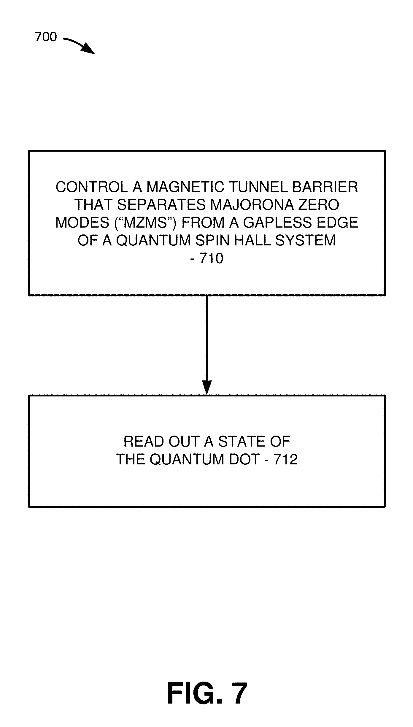
[0034] FIG. 7 is a flow chart 700 illustrating an example embodiment for operating quantum device. The illustrated actions are shown by way of example only, as any one or more of the actions may be omitted in certain embodiments, performed in a different sequence, performed concurrently, or replaced by some other actions. Also, additional actions may also be included that are not illustrated here.
[0035] At 710, a magnetic tunnel barrier is controlled that separates Majorona zero modes ("MZMs") from an edge area (e.g., a gapless edge) of a quantum spin hall system. In certain embodiments, the magnetic tunnel barrier is formed from a pair of magnetic insulators whose magnetization is held constant, and the magnetic tunnel barrier is tuned by controlling a gate controlling the electron density around the magnetic insulator in the QSH plane, thereby forming a quantum dot.
[0036] At 712, a state of the quantum dot is read out (e.g., using a charge sensor as disclosed herein).
[0037] In some embodiments, the quantum spin hall system implements a tetron qubit. In further implementations, the tetron qubit does not comprise a Josephson junction. In some implementations, the tunable quantum dot is further located between or substantially between two magnetic insulators (e.g., in some implementations, the two magnetic insulators are non-tunable).
[0038] In further embodiments, the quantum spin hall system implements a hexon qubit. In some implementations, the hexon qubit does not comprise a Josephson junction. In certain implementations, the tunable quantum dot is further located between or substantially between two magnetic insulators (e.g., in some implementations, the two magnetic insulators are non-tunable).
[0039] Further embodiments comprise a tetron qubit that comprises three pairs of Majorana zero modes, wherein the tetron qubit further comprises a tunable quantum dot configured to control a magnetic tunnel barrier between two neighboring Majorana zero modes. In some embodiments, the tetron qubit does not comprise a Josephson junction. In certain embodiments, the tunable quantum dot is further located between or substantially between two magnetic insulators (e.g., in some implementations, the two magnetic insulators are non-tunable). In further embodiments, the tetron qubit is part of a topologically protected quantum computing system.
[0040] Still further embodiments comprise a hexon qubit comprising four pairs of Majorana zero modes, wherein the hexon qubit further comprises a tunable quantum dot configured to control a magnetic tunnel barrier between two neighboring Majorana zero modes. In some embodiments, the hexon qubit does not comprise a Josephson junction. In certain embodiments, the tunable quantum dot is further located between or substantially between two magnetic insulators (e.g., in some implementations, the two magnetic insulators are non-tunable). In further embodiments, the hexon qubit is part of a topologically protected quantum computing system.
III. Concluding Remarks
[0041] Example designs for Majorana tetron qubits (sometimes also referred to as "quad qubits") and Majorana hexon qubits that can be realized with and/or otherwise incorporate the disclosed technology are described in, for example, Karzig et al., "Scalable Designs for Quasiparticle-Poisoning-Protected Topological Quantum Computation with Majorana Zero Modes," arXiv:1610.05289 (March 2017) and T. Karzig et al., "Scalable Designs for Quasiparticle-Poisoning-Protected Topological Quantum Computation with Majorana Zero Modes," Phys. Rev. B 95, 235305 (2017); U.S. patent application Ser. No. 15/636,457 entitled "QUANTUM COMPUTING METHODS AND DEVICES FOR MAJORANA QUAD QUBITS" and filed on Jun. 28, 2017 (published as U.S. Patent Application Publication No. 2018/0052806); U.S. patent application Ser. No. 15/636,376 entitled "QUANTUM COMPUTING DEVICES WITH MAJORANA HEXON QUBITS" and filed on Jun. 28, 2017 (published as U.S. Patent Application Publication No. 2018/0053809); U.S. Provisional Application No. 62/382,253, entitled "QUANTUM COMPUTING DEVICES WITH MAJORANA HEXON QUBITS" filed on Aug. 31, 2016; and U.S. Provisional Application No. 62/385,245, entitled "QUANTUM COMPUTING METHODS AND DEVICES FOR MAJORANA QUAD QUBITS" filed on Sep. 8, 2016, all of which are incorporated herein by reference in their entirety.
[0042] The disclosed methods, apparatus, and systems should not be construed as limiting in any way. Instead, the present disclosure is directed toward all novel and nonobvious features and aspects of the various disclosed embodiments, alone and in various combinations and sub combinations with one another. The disclosed methods, apparatus, and systems are not limited to any specific aspect or feature or combination thereof, nor do the disclosed embodiments require that any one or more specific advantages be present or problems be solved.
[0043] The technologies from any example can be combined with the technologies described in any one or more of the other examples. In view of the many possible embodiments to which the principles of the disclosed technology may be applied, it should be recognized that the illustrated embodiments are examples of the disclosed technology and should not be taken as a limitation on the scope of the disclosed technology.
* * * * *
D00000
D00001
D00002
D00003
D00004
D00005
D00006
D00007
XML
uspto.report is an independent third-party trademark research tool that is not affiliated, endorsed, or sponsored by the United States Patent and Trademark Office (USPTO) or any other governmental organization. The information provided by uspto.report is based on publicly available data at the time of writing and is intended for informational purposes only.
While we strive to provide accurate and up-to-date information, we do not guarantee the accuracy, completeness, reliability, or suitability of the information displayed on this site. The use of this site is at your own risk. Any reliance you place on such information is therefore strictly at your own risk.
All official trademark data, including owner information, should be verified by visiting the official USPTO website at www.uspto.gov. This site is not intended to replace professional legal advice and should not be used as a substitute for consulting with a legal professional who is knowledgeable about trademark law.