Perpendicular Magnetic Tunnel Junction Device With Skyrmionic Enhancement Layers For The Precessional Spin Current Magnetic Laye
Schabes; Manfred Ernst ; et al.
U.S. patent application number 15/862788 was filed with the patent office on 2019-07-11 for perpendicular magnetic tunnel junction device with skyrmionic enhancement layers for the precessional spin current magnetic laye. The applicant listed for this patent is Spin Memory, Inc.. Invention is credited to Bartlomiej Adam Kardasz, Mustafa Michael Pinarbasi, Manfred Ernst Schabes.
| Application Number | 20190214548 15/862788 |
| Document ID | / |
| Family ID | 67139185 |
| Filed Date | 2019-07-11 |


| United States Patent Application | 20190214548 |
| Kind Code | A1 |
| Schabes; Manfred Ernst ; et al. | July 11, 2019 |
PERPENDICULAR MAGNETIC TUNNEL JUNCTION DEVICE WITH SKYRMIONIC ENHANCEMENT LAYERS FOR THE PRECESSIONAL SPIN CURRENT MAGNETIC LAYER
Abstract
A magnetoresistive random-access memory (MRAM) is disclosed. The MRAM device includes a perpendicular magnetic tunnel junction device having a reference layer, a free layer, and a precessional spin current magnetic layer. A skyrmionic enhancement layer is provided adjacent to the precessional spin current magnetic layer. The skyrmionic enhancement layer helps to improve the response of the precessional spin current magnetic layer to applied spin polarized currents.
| Inventors: | Schabes; Manfred Ernst; (Saratoga, CA) ; Pinarbasi; Mustafa Michael; (Morgan Hill, CA) ; Kardasz; Bartlomiej Adam; (Pleasanton, CA) | ||||||||||
| Applicant: |
|
||||||||||
|---|---|---|---|---|---|---|---|---|---|---|---|
| Family ID: | 67139185 | ||||||||||
| Appl. No.: | 15/862788 | ||||||||||
| Filed: | January 5, 2018 |
| Current U.S. Class: | 1/1 |
| Current CPC Class: | G11C 11/161 20130101; H01F 10/329 20130101; H01L 43/10 20130101; H01L 43/12 20130101; H01F 10/3286 20130101; H01L 43/08 20130101; H01L 43/02 20130101; H01F 41/307 20130101; H01F 10/3272 20130101; B82Y 25/00 20130101; H01L 27/222 20130101 |
| International Class: | H01L 43/08 20060101 H01L043/08; H01L 43/12 20060101 H01L043/12; H01L 43/10 20060101 H01L043/10; H01L 27/22 20060101 H01L027/22; H01L 43/02 20060101 H01L043/02 |
Claims
1. A magnetic device, comprising: a first synthetic antiferromagnetic structure in a first plane having a magnetization vector that is perpendicular to the first plane and having a fixed magnetization direction; an antiferromagnetic coupling layer in a second plane and disposed above the first synthetic antiferromagnetic structure; a second synthetic antiferromagnetic structure in a third plane and disposed over the antiferromagnetic coupling layer; a magnetic reference layer in a fourth plane and disposed over the second synthetic antiferromagnetic structure, the magnetic reference layer having a magnetization vector that is perpendicular to the fourth plane and having a fixed magnetization direction; a non-magnetic tunnel barrier layer in a fifth plane and disposed over the magnetic reference layer; a free magnetic layer disposed in a sixth plane over the non-magnetic tunnel barrier layer, the free magnetic layer having a magnetization vector that is perpendicular to the sixth plane and having a magnetization direction that can switch between a first magnetization direction to a second magnetization direction, the magnetic reference layer, the non-magnetic tunnel barrier layer and the free magnetic layer forming a magnetic tunnel junction; a precessional spin current magnetic layer disposed in a seventh plane that is physically separated from the free magnetic layer and coupled to the free magnetic layer by a filter coupling layer that may induce ferromagnetic or antiferromagnetic coupling between the free magnetic layer and the precessional spin current layer; and a skyrmionic enhancement layer disposed in an eighth plane over the precessional spin current magnetic layer and being formed from a heavy metal with large spin-orbit coupling such that the skyrmionic enhancement layer induces a Dzyaloshinskii-Moriya interaction at an interface between the precessional spin current magnetic layer and the skyrmionic enhancement layer thereby creating a non-collinear magnetic texture in the precessional spin current magnetic layer near the interface.
2. The magnetic device of claim 1, wherein the skyrmionic enhancement layer is formed of tungsten, iridium, palladium, gold, platinum, or alloys thereof.
3. The magnetic device of claim 1, wherein the skyrmionic enhancement layer is formed from a single layer of metal.
4. The magnetic device of claim 3, wherein a thickness of the skyrmionic enhancement layer is in the range of 0.3 nm to 4 nm.
5. The magnetic device of claim 1, wherein the skyrmionic enhancement layer includes multiple layers of metal.
6. The magnetic device of claim 5, wherein a thickness of the skyrmionic enhancement layer is in the range of 0.6 nm to 12 nm.
7. The magnetic device of claim 5, wherein the skyrmionic enhancement layer includes alternating first and second layers, wherein the first layers are formed of tungsten, iridium, palladium, gold, platinum, or alloys thereof, and wherein the second layers are formed of iron, cobalt, nickel, or alloys thereof.
8. A magnetic device, comprising: a magnetic reference layer in a first plane, the magnetic reference layer having a magnetization vector that is perpendicular to the first plane and having a fixed magnetization direction; a non-magnetic tunnel barrier layer in a second plane and disposed over the magnetic reference layer; a free magnetic layer disposed in a third plane over the non-magnetic tunnel barrier layer, the free magnetic layer having a magnetization vector that is perpendicular to the third plane and having a magnetization direction that can switch between a first magnetization direction to a second magnetization direction, the magnetic reference layer, the non-magnetic tunnel barrier layer and the free magnetic layer forming a magnetic tunnel junction; a precessional spin current magnetic layer disposed in a fourth plane that is physically separated from the free magnetic layer and coupled to the free magnetic layer by a filter coupling layer that may induce ferromagnetic or antiferromagnetic coupling between the free magnetic layer and the precessional spin current magnetic layer; and a skyrmionic enhancement layer disposed in a fifth plane over the precessional spin current magnetic layer and being formed from a heavy metal with large spin-orbit coupling such that the skyrmionic enhancement layer induces a Dzyaloshinskii-Moriya interaction at an interface between the precessional spin current magnetic layer and the skyrmionic enhancement layer thereby creating a non-collinear magnetic texture in the precessional spin current magnetic layer near the interface.
9. The magnetic device of claim 8, wherein the skyrmionic enhancement layer is formed of tungsten, iridium, platinum, gold, palladium, or alloys thereof.
10. The magnetic device of claim 8, wherein the skyrmionic enhancement layer is formed of tungsten.
11. The magnetic device of claim 8, wherein the skyrmionic enhancement layer is formed of iridium.
12. The magnetic device of claim 8, wherein the skyrmionic enhancement layer is formed of platinum.
13. The magnetic device of claim 8, wherein the skyrmionic enhancement layer is formed of gold.
14. The magnetic device of claim 8, wherein the skyrmionic enhancement layer is formed of palladium.
15. The magnetic device of claim 8, wherein the skyrmionic enhancement layer is formed from a single layer of metal.
16. The magnetic device of claim 15, wherein a thickness of the skyrmionic enhancement layer is in the range of 0.3 nm to 4 nm.
17. The magnetic device of claim 8, wherein the skyrmionic enhancement layer includes multiple layers of metal.
18. The magnetic device of claim 17, wherein a thickness of the skyrmionic enhancement layer is in the range of 0.6 nm to 12 nm.
19. The magnetic device of claim 17, wherein the skyrmionic enhancement layer includes alternating first and second layers, wherein the first layers are formed of tungsten, iridium, palladium, gold, platinum, or alloys thereof, and wherein the second layers are formed of iron, cobalt, nickel, or alloys thereof.
20. A method for manufacturing a magnetic device comprising the steps of: providing a magnetic tunnel junction including a magnetic reference layer, a non-magnetic tunnel barrier layer, and a free magnetic layer; depositing a filter coupling layer over the free magnetic layer; depositing a precessional spin current magnetic layer over the filter coupling layer; depositing a skyrmionic enhancement layer over the precessional spin current layer; depositing an electrical contact layer over the skyrmionic enhancement layer; and forming a pillar that includes the skyrmionic enhancement layer, the precessional spin current magnetic layer, the filter coupling layer, the free magnetic layer, the non-magnetic tunnel barrier layer, and the magnetic reference layer.
Description
CROSS-REFERENCE TO RELATED APPLICATIONS
[0001] Cross-reference is made to the following related applications, all of which are filed concurrently herewith, incorporated herein by reference, and assigned to assignee of this patent document: U.S. application Ser. No. ______ [Attorney Dkt. No. 1058410-00067], entitled "SWITCHING AND STABILITY CONTROL FOR PERPENDICULAR MAGNETIC TUNNEL JUNCTION DEVICE," U.S. application Ser. No. ______ [Attorney Dkt. No. 1058410-00065], entitled "PERPENDICULAR MAGNETIC TUNNEL JUNCTION DEVICE WITH OFFSET PRECESSIONAL SPIN CURRENT LAYER," U.S. application Ser. No. ______ [Attorney Dkt. No. 1058410-00064], entitled "PERPENDICULAR MAGNETIC TUNNEL JUNCTION DEVICE WITH PRECESSIONAL SPIN CURRENT LAYER HAVING A MODULATED MOMENT DENSITY," and U.S. application Ser. No. ______ [Attorney Dkt. No. 1058410-00063], entitled "PERPENDICULAR MAGNETIC TUNNEL JUNCTION DEVICE WITH SKYRMIONIC ASSIST LAYERS FOR FREE LAYER SWITCHING."
FIELD
[0002] The present patent document relates generally to magnetic random access memory and, more particularly, to a device having a skyrmionic enhancement layer to provide the device with quicker, better optimized, or more efficient responses to applied spin polarized currents.
BACKGROUND
[0003] Magnetoresistive random-access memory ("MRAM") is a non-volatile memory technology that stores data through magnetic storage elements. These elements are two ferromagnetic plates or electrodes that can hold magnetization and are separated by a non-magnetic material, such as a non-magnetic metal or insulator. In general, one of the plates has its magnetization pinned (i.e., a "reference layer"), meaning that this layer has a higher coercivity than the other layer and requires a larger magnetic field or spin-polarized current to change the orientation of its magnetization. The second plate is typically referred to as the free layer and its magnetization direction can be changed by a smaller magnetic field or spin-polarized current relative to the reference layer.
[0004] MRAM devices store information by changing the orientation of the magnetization of the free layer. In particular, based on whether the free layer is in a parallel or anti-parallel alignment relative to the reference layer, either a "1" or a "0" can be stored in each MRAM cell. Due to the spin-polarized electron tunneling effect, the electrical resistance of the cell changes due to the orientation of the magnetization of the two layers. The cell's resistance will be different for the parallel and anti-parallel states and thus the cell's resistance can be used to distinguish between a "1" and a "0." One important feature of MRAM devices is that they are non-volatile memory devices, since they maintain the information even when the power is off. The two plates can be sub-micron in lateral size and the magnetization direction can still be stable with respect to thermal fluctuations.
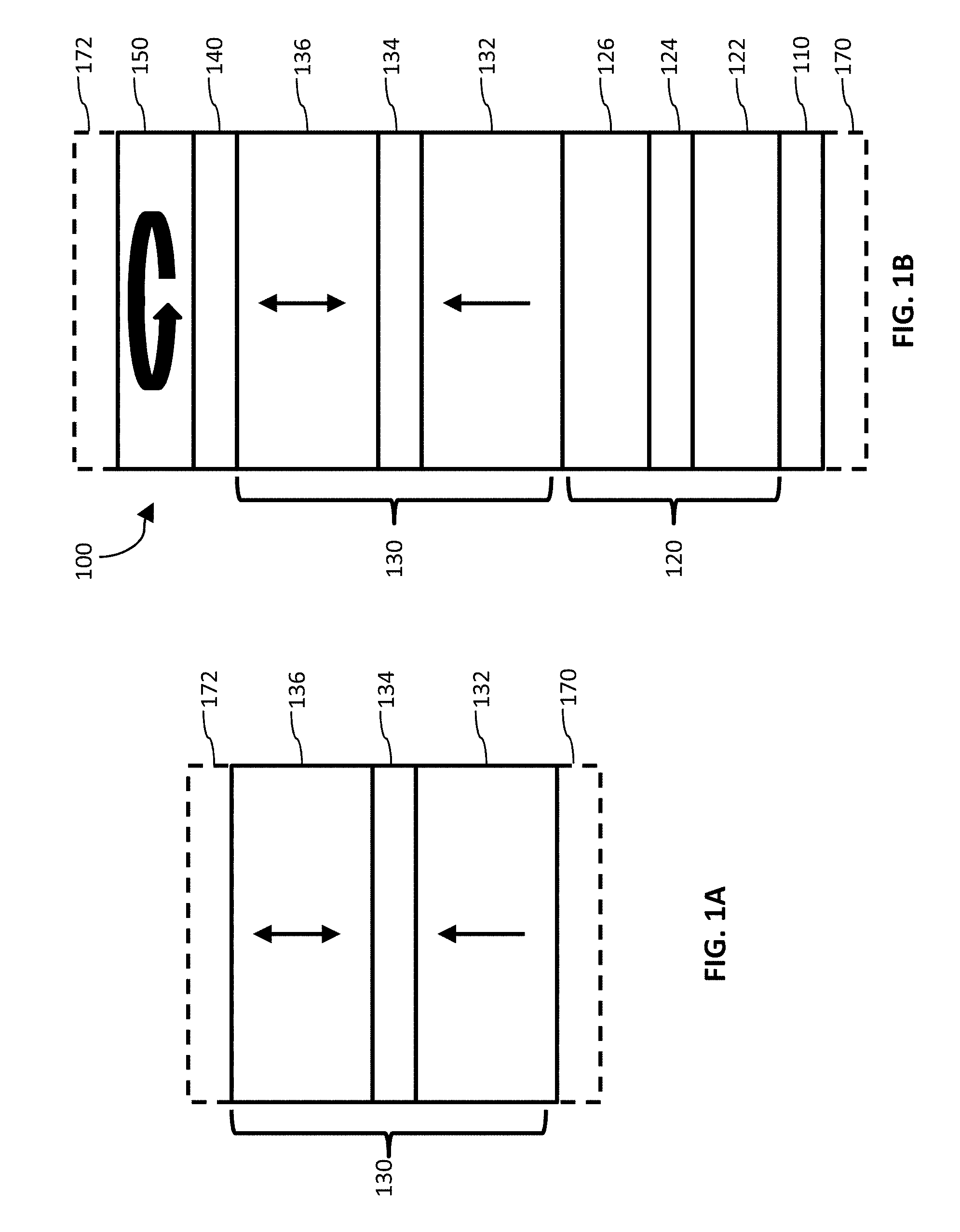
[0005] FIG. 1A illustrates a magnetic tunnel junction ("MTJ") 130 for a conventional MRAM device. The MTJ 130 includes reference layer 132, which is a magnetic layer, a non-magnetic tunneling barrier layer 134, which generally is an insulator at large layer thickness but at small layer thickness admits the flow of an appreciable quantum mechanical tunnel current, and a free layer 136, which is also a magnetic layer. The magnetization direction of the magnetic layers of the MTJ 130 can either be in the planes of those layers or perpendicular to the planes of those layers. As shown in FIG. 1A, the magnetic reference layer 132 has a magnetization direction perpendicular to its plane. Also as seen in FIG. 1A, the free layer 136 also has a magnetization direction perpendicular to its plane, but its direction can vary by 180 degrees. Because the magnetization direction of the magnetic layers of the MTJ 130 is perpendicular to the planes of those layers, the MTJ 130 shown in FIG. 1A is known as a perpendicular MTJ ("pMTJ").
[0006] As shown in FIG. 1A, electrical contact layers 170, 172 can optionally be used to provide electrical contact to the MTJ 130. When the magnetization of the free layer 136 is oriented in a direction parallel to the magnetization direction of the reference layer 132, electrons will be more likely to tunnel across the tunneling barrier layer 134, and thus resistance across the MTJ 130 will be lower. Alternatively, when the magnetization of the free layer 136 is oriented in a direction that is anti-parallel to the magnetization direction of the reference layer 132, electrons will be less likely to tunnel across the tunneling barrier layer 134, making the resistance across the MTJ 130 significantly higher. It is these different resistances that can be used to distinguish and store a digital "1" or "0" bit.
[0007] The MTJ 130 may also form part of a larger MTJ stack 100, as shown in FIG. 1B, which may include a number of other optional layers that can be used to facilitate operation of the MTJ. As described in connection with FIG. 1A, the MTJ stack 100 of FIG. 1B may include electrical contact layers 170, 172 for providing electrical contact across the MTJ stack 100, including the MTJ 130. The MTJ 130 may be disposed above an antiferromagnetic layer or a synthetic antiferromagnetic ("SAF") structure 120, which may include multiple layers as shown in FIG. 1B. For example, as shown in FIG. 1B, the SAF structure 120 may include two or more thin magnetic layers, including a lower "SAF1" layer 122 and an upper "SAF2" layer 126 having opposite or anti-parallel magnetization directions separated by an antiferromagnetic coupling layer 124 or spacer layer that is not magnetic. The SAF structure 120 also may be formed over a seed layer 110, as shown in FIG. 1B, and over a substrate (not shown). Note that as used herein, terms such as "lower," "upper," "top," "bottom," and the like are provided for convenience in explaining the various embodiments, and are not limiting in any way.
[0008] Spin transfer torque or spin transfer switching, may be used in connection with an MTJ 130. In such a configuration, a filter layer 150 may be used to alter the spin of electrons passing through the MTJ 130. For example, the filter layer may be a polarizer layer designed to further align the spin of electrons (i.e., to further "polarize" the electrons) passing through the MTJ 130 beyond the alignment already provided by the reference layer 132. U.S. patent application Ser. No. 14/814,036, filed by Pinarbasi et al., and assigned to the assignee of this patent document describes using a polarizer layer. The disclosure of U.S. patent application Ser. No. 14/814,036 is incorporated herein by reference in its entirety. The spin-aligned or "polarized" electrons are used to change the magnetization orientation of the free layer 136 in the MTJ 130. In general, electrons possess a spin, a quantized number of angular momentum intrinsic to the electron. An electrical current is generally unpolarized, i.e., it consists of 50% spin up and 50% spin down electrons. Passing a current though a magnetic layer, like the filter layer 150 or the reference layer 132, polarizes electrons with the spin orientation corresponding to the magnetization direction of the magnetic layer, thus producing a spin-polarized current. If a spin-polarized current is passed to the magnetic region of a free layer 136 of the MTJ 130, the electrons will transfer a portion of their spin-angular momentum to the free layer to produce a torque on the magnetization of the free layer. Thus, this spin transfer torque can switch the magnetization of the free layer, and can be used to write either a "1" or a "0" based on whether the free layer 136 is in the parallel or anti-parallel states relative to the reference layer.
[0009] As shown in FIG. 1B, the filter layer 150 and a filter coupling layer 140 are disposed above the free layer 136 of the MTJ 130. The filter layer 150 is physically separated from the free layer 136 and is coupled to the free layer 136 by the filter coupling layer 140. The filter layer 150 can be used to polarize a current of electrons ("spin-aligned electrons") applied to MTJ structure 100 in the manner described above.
[0010] The filter layer 150 may be a precessional spin current ("PSC") magnetic layer, an example of which is described in detail in U.S. patent application Ser. No. 14/814,036, filed by Pinarbasi et al., and assigned to the assignee of this patent document. Additionally, a precessional spin current structure for MRAM is described in U.S. patent application Ser. Nos. 15/445,260 and 15/445,362, both of which are filed by Pinarbasi et al. and are assigned to the assignee of this patent document. The disclosures of U.S. patent application Ser. Nos. 15/445,260 and 15/445,362 are both incorporated herein by reference in their entireties.
[0011] In an MRAM device, the incubation period (the time required to initiate the switching of the free layer) can dominate the total switching time of the MRAM device. Shortening incubation periods therefore increases the switching speed or, conversely, lowers the switching current and is thus is advantageous for the operation of MRAM devices.
[0012] In conventional MRAM devices, the initiation of the switching of the free layer may depend on thermal fluctuations that overcome the energy barrier due to the perpendicular magnetic anisotropy ("PMA") at the interface between the free layer and the tunnel barrier layer.
[0013] In an MRAM device having a precessional spin current layer, the dynamic properties of the precessional spin current layer are important for the optimal performance of the MRAM device. The ability of the precessional spin current layer to respond efficiently to spin polarized currents can improve the overall performance of the MRAM device in terms of higher switching speed and/or lower switching currents.
[0014] In an MRAM devices having a precessional spin current layer, the magnetic motion of the precessional spin current layer is generally affected by anisotropies of its magnetic materials, the magnetic shape anisotropy, interface energies, as well as energy barriers created by local imperfections of the materials, surfaces, and interfaces included by the precessional spin current layer.
SUMMARY
[0015] An MRAM device is disclosed that has one or more auxiliary layers to facilitate the local canting of electronic spins via the Dzyaloshinskii-Moriya interaction ("DMI") near the surface of the free layer and/or near the surface of precessional spin current layers. These auxiliary layers are referred to as skyrmionic enhancement layers because it is well known in the art that the DMI can lead to non-collinear atomic spin textures, which can promote the formation of skyrmions in various bulk and multilayer materials. A skyrmionic enhancement layer may be adjacent to the free layer and may help to initiate the switching of the free layer. The skyrmionic enhancement layer may, for example, help to reduce incubation periods and thereby increase the switching speed of an MRAM device, or it may reduce the amount of required switching current and thereby increase the endurance (number of switching cycles during the useful life of the device) of an MRAM device.
[0016] The DMI is generated at the free layer by forming a skyrmionic enhancement layer in a plane, preferably directly above the free layer. The skyrmionic enhancement layer may comprise a non-magnetic heavy metal with large spin-orbit coupling, such as tungsten (W), iridium (Ir), palladium (Pd), gold (Au), or platinum (Pt), or suitable alloys thereof, or suitable multilayers comprising alternating thin layers of said metals and magnetic metals such as iron (Fe), cobalt (Co), nickel (Ni), or suitable alloys thereof. DMI at the free layer results from the spin-orbit coupling and the broken symmetry at the interface of the skyrmionic enhancement layer and the free layer. In the case of a multilayer skyrmionic enhancement layer, additional DMI results from the spin-orbit coupling and the broken symmetry at one or more of the internal interfaces within the multilayer. In the case of a multilayer skyrmionic enhancement layer, the multilayer is formed in such sequence that one of the magnetic layers is in direct contact with the free layer.
[0017] The skyrmionic enhancement layer facilitates the local canting of atomic spins relative to the perpendicular direction near the interface of the skyrmionic layer and the free layer, and thereby increases the effectiveness of spin polarized switching currents to produce spin torques during the initiation of the free-layer switching because spin torques are generally proportional to sin(.theta.), where .theta. is the angle between the direction of the polarization of the spin-polarized current and the local magnetic moment of the free layer.
[0018] Generally, the DMI can be large at interfaces of magnetic material with a non-magnetic heavy metal with large spin orbit coupling. For example, the DMI reaches about 2 mJ/m.sup.2 in the case of Ir|Co|Pt multilayers, as shown by C. Moreau-Luchaire et al., in the paper "Skyrmions at room temperature: From magnetic thin films to magnetic multilayers" arXiv:1502.07853, which is incorporated herein by reference in its entirety. There are many other papers that describe the fundamental physics of the DMI and DMI-induced non-collinear spin textures such as skyrmions, including recent scientific reviews such as the paper by W. Jiang et al., Phys. Rep. 704 (2017), 1-49, or the paper by F. Hellman et al., Rev. Mod. Phys. 89, 025006 (2017), as will be readily understood by a person skilled in the art.
[0019] In an MRAM device having a precessional spin current layer, a skyrmionic enhancement layer is formed in a plane, preferably directly above the precessional spin current layer, to help initiate the magneto-dynamic motion of the precessional spin current layer via the DMI at the interface between the skyrmionic enhancement layer and the precessional spin current layer. The skyrmionic enhancement layer is comprised of a non-magnetic heavy metal with large spin-orbit coupling, such as tungsten (W), iridium (Ir), palladium (Pd), gold (Au), or platinum (Pt), or suitable alloys thereof, or of suitable multilayers comprised of alternating thin layers of said heavy non-magnetic metals and magnetic metals such as iron (Fe), cobalt (Co), nickel (Ni), or suitable alloys thereof.
[0020] The DMI at the precessional spin current layer results from the spin-orbit coupling and the broken symmetry at the interface of the skyrmionic enhancement layer and the precessional spin current layer. In the case of a multilayer skyrmionic enhancement layer, additional DMI results from the spin-orbit coupling and the broken symmetry at one or more of the internal interfaces within the multilayer. In the case of a multilayer skyrmionic enhancement layer, the multilayer is formed in such sequence that one of the magnetic layers is in direct contact with the precessional spin current layer.
[0021] The skyrmionic enhancement layer facilitates the local canting of atomic spins relative to the perpendicular direction near the interface of the skyrmionic enhancement layer and the precessional spin current layer and thereby increases the effectiveness of spin polarized switching currents to produce spin torques during the initiation of the free-layer switching because spin torques generally are proportional to sin(.theta.), where .theta. is the angle between the direction of the polarization of the spin-polarized current and the local magnetic moment of the precessional spin current layer. The skyrmionic enhancement layer thus promotes a local non-collinear magnetic texture in the precessional spin current layer near the interface of the skyrmionic enhancement layer and the precessional spin current layer. In this way the DMI may help to overcome deleterious pinning effects due to local imperfections in the materials, interfaces, and surfaces of the precessional spin current layer.
[0022] In an embodiment, a magnetic device may include a first synthetic antiferromagnetic structure in a first plane having a magnetization vector that is perpendicular to the first plane and having a fixed magnetization direction. An embodiment may also include an antiferromagnetic coupling layer in a second plane and disposed above the first synthetic antiferromagnetic structure and a second synthetic antiferromagnetic structure in a third plane and disposed over the antiferromagnetic coupling layer. An embodiment further includes a magnetic reference layer in a fourth plane and disposed over the second synthetic antiferromagnetic structure. The magnetic reference layer has a magnetization vector that is perpendicular to the fourth plane and has a fixed magnetization direction. (For the purposes of this patent document, angles within several degrees of perpendicular are within the scope of what is considered perpendicular.) An embodiment further includes a non-magnetic tunnel barrier layer in a fifth plane and disposed over the magnetic reference layer. An embodiment also includes a free magnetic layer disposed in a sixth plane over the non-magnetic tunnel barrier layer. The free magnetic layer has a magnetization vector that is perpendicular to the sixth plane and has a magnetization direction that can switch between a first magnetization direction to a second magnetization direction. The magnetic reference layer, the non-magnetic tunnel barrier layer and the free magnetic layer form a magnetic tunnel junction.
[0023] In an embodiment of the magnetic device, a skyrmionic enhancement layer is disposed in a plane over the free magnetic layer and is formed from a heavy metal with large spin-orbit coupling such that the skyrmionic enhancement layer induces a Dzyaloshinskii-Moriya interaction at an interface between the free layer and the skyrmionic enhancement layer thereby creating local canting of the atomic spins or a non-collinear magnetic texture in the free magnetic layer near the interface.
[0024] In an alternate embodiment, a skyrmionic enhancement layer disposed in a plane over the free layer and is formed from a multilayer comprised of alternating thin layers of a non-magnetic heavy metal with large spin-orbit coupling, such as tungsten (W), iridium (Ir), palladium (Pd), gold (Au), or platinum (Pt), and thin layers of magnetic metals such as iron (Fe), cobalt (Co), or nickel (Ni) or suitable alloys thereof. The DMI at the free layer results from the spin-orbit coupling and the broken symmetry at one or more of the internal interfaces within the multilayer. The multilayer skyrmionic enhancement layer is formed in such sequence that one of the magnetic layers is in direct contact with the free layer thereby transmitting the transmitting DMI torques to the free layer, and thereby creating local canting of the atomic spins or a non-collinear magnetic texture in the free layer near the interface between the skyrmionic enhancement layer and the free layer.
[0025] In an embodiment of the magnetic device, a precessional spin current layer is disposed in a plane that is physically separated from the free magnetic layer and coupled to the free magnetic layer by a filter coupling layer that may induce ferromagnetic or antiferromagnetic coupling between the free magnetic layer and the precessional spin current magnetic layer. A skyrmionic enhancement layer is disposed in a plane over the precessional spin current layer and is formed from a heavy metal with large spin-orbit coupling, such as tungsten (W), iridium (Ir), gold (Au), palladium (Pd), or platinum (Pt) or suitable alloys thereof, such that the skyrmionic enhancement layer induces a Dzyaloshinskii-Moriya interaction at an interface between the precessional spin current magnetic layer and the skyrmionic enhancement layer thereby creating local canting of the atomic spins or a non-collinear magnetic texture in the free magnetic layer spins near the interface between the skyrmionic enhancement layer and the precessional spin current layer.
[0026] In an alternate embodiment of an MRAM device, a precessional spin current layer is disposed in a plane that is physically separated from the free magnetic layer and coupled to the free magnetic layer by a filter coupling layer that may induce ferromagnetic or antiferromagnetic coupling between the free magnetic layer and the precessional spin current magnetic layer. Additionally, a multilayer skyrmionic enhancement layer is disposed in a plane, preferably above the precessional spin current layer. The multilayer skyrmionic enhancement layer is formed from a multilayer comprised of alternating thin layers of a non-magnetic heavy metal with large spin-orbit coupling, such as tungsten (W), iridium (Ir), gold (Au), palladium (Pd), or platinum (Pt), or suitable alloys thereof, and magnetic metals such as iron (Fe), cobalt (Co), nickel (Ni), or suitable alloys thereof. Dzyaloshinskii-Moriya interaction is generated at the precessional spin current layer due to the spin-orbit coupling and the broken symmetry at the interface between the precessional spin current layer and the skyrmionic enhancement layer. Additional DMI is generated at one or more of the internal interfaces within the multilayer. The multilayer skyrmionic enhancement layer is formed in such sequence that one of the magnetic layers is in direct contact with the precessional spin current layer thereby transmitting DMI torques to the precessional spin current layer, and thereby creating local canting of the atomic spins or a non-collinear magnetic texture in the precessional spin current layer spins near the interface between the skyrmionic enhancement layer and the precessional spin current layer.
BRIEF DESCRIPTION OF THE DRAWINGS
[0027] The accompanying drawings, which are included as part of the present specification, illustrate the presently preferred embodiments and, together with the general description given above and the detailed description given below, serve to explain and teach the principles of the MTJ devices described herein.
[0028] FIG. 1A illustrates a conventional MTJ capable of use in an MRAM device.
[0029] FIG. 1B illustrates a conventional MTJ stack for an MRAM device.
[0030] FIG. 2 illustrates an MTJ stack for an MRAM device with a skyrmionic enhancement layer provided above the free layer.
[0031] FIG. 3 illustrates an MTJ stack for an MRAM device with a precessional spin current layer and a skyrmionic enhancement layer provided above the precessional spin current layer.
[0032] FIG. 4 illustrates a flow chart showing manufacturing steps for an MRAM device in accordance with embodiments.
[0033] FIG. 5 illustrates a flow chart showing manufacturing steps for an MRAM device in accordance with embodiments.
[0034] FIG. 6 illustrates a flow chart showing manufacturing steps for an MRAM device in accordance with embodiments.
[0035] The figures are not necessarily drawn to scale and the elements of similar structures or functions are generally represented by like reference numerals for illustrative purposes throughout the figures. The figures are only intended to facilitate the description of the various embodiments described herein; the figures do not describe every aspect of the teachings disclosed herein and do not limit the scope of the claims.
DETAILED DESCRIPTION
[0036] The following description is presented to enable any person skilled in the art to create and use a skyrmionic enhancement layer for a pMTJ device that serves to improve high-speed performance of the device. Each of the features and teachings disclosed herein can be utilized separately or in conjunction with other features to implement the disclosed system and method. Representative examples utilizing many of these additional features and teachings, both separately and in combination, are described in further detail with reference to the attached drawings. This detailed description is merely intended to teach a person of skill in the art further details for practicing preferred aspects of the present teachings and is not intended to limit the scope of the claims. Therefore, combinations of features disclosed in the following detailed description may not be necessary to practice the teachings in the broadest sense, and are instead taught merely to describe particularly representative examples of the present teachings.
[0037] In the following description, for purposes of explanation only, specific nomenclature is set forth to provide a thorough understanding of the present teachings. However, it will be apparent to one skilled in the art that these specific details are not required to practice the present teachings.
[0038] This patent document discloses a skyrmionic enhancement layer for a pMTJ device that may improve the response of the free layer or a precessional spin current layer to applied spin polarized currents. According to an embodiment, a skyrmionic enhancement layer is provided adjacent to a free layer, and helps initiate switching of the free layer by reducing incubation periods. According to another embodiment, a skyrmionic enhancement layer is provided adjacent to a precessional spin current layer, and helps improve high-speed performance of the MTJ by accelerating the magneto-dynamic response of the precessional spin current layer.
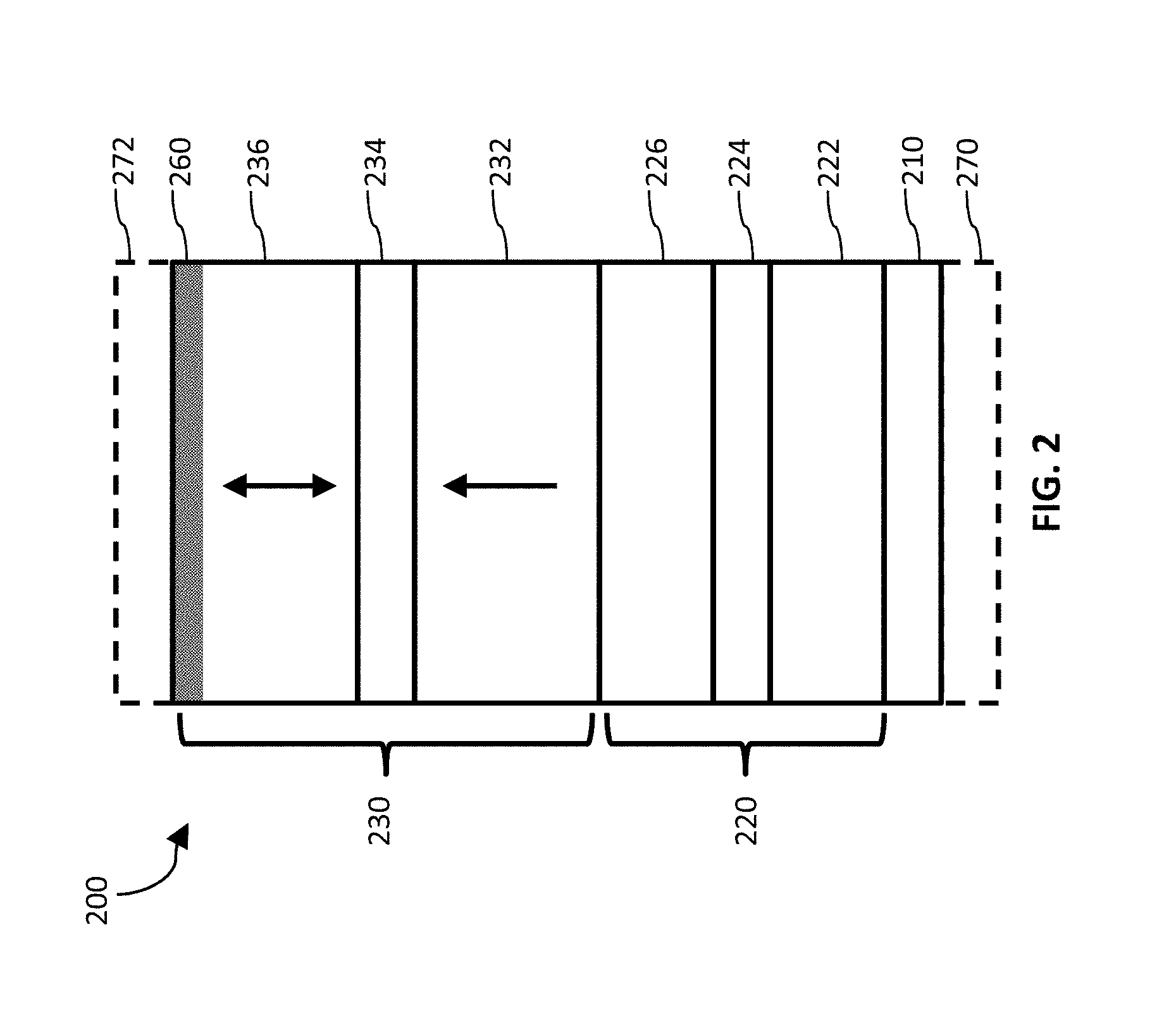
[0039] FIG. 2 shows an MTJ stack 200 that can be used as an MRAM device. The MTJ stack 200 includes an MTJ 230, which includes a magnetic reference layer 232, a non-magnetic tunneling barrier layer 234, and a magnetic free layer 236. The magnetic reference layer 232 has a magnetization direction perpendicular to its plane, and the free layer 236 also has a magnetization direction perpendicular to its plane, but as shown in FIG. 2, its direction can vary by 180 degrees. The differences in resistance based on whether the magnetization direction of the free layer 236 is parallel to or anti-parallel to the magnetization direction of the reference layer 232 can be used to distinguish and store a digital "1" or "0" bit. The non-magnetic tunneling barrier layer 234 may be formed from MgO, or other suitable material. In embodiments where MgO is used to form the tunneling barrier layer 234, that material may have a crystalline texture that is a (001) texture.
[0040] The MTJ stack 200 may also include a number of other optional layers that can be used to facilitate operation of the MTJ 230. For example, the MTJ stack 200 may include electrical contact layers 270, 272 for providing electrical contact across the MTJ stack 200. According to an embodiment, the electrical contact layers 270, 272 may be electrodes for providing a voltage across the MTJ stack 200, and may be formed from any suitable conducting material. The MTJ 230 also can be disposed above an SAF structure 220, which may include multiple sub-layers and structures as shown in FIG. 2. For example, as shown in FIG. 2, the SAF structure 220 may include two or more thin magnetic layers, such as a lower "SAF1" layer 222 and an upper "SAF2" layer 226, having opposite or anti-parallel magnetization directions separated by an antiferromagnetic coupling layer 224 (or "spacer" layer) that is not magnetic. The SAF structure 220 also may be formed over a seed layer 210 and over a substrate (not shown). In general, in each of the MTJ stacks described herein, the lower SAF1 layer of the MTJ can be formed on a seed layer, as shown in FIG. 2 and the other figures using similar numbering, and all layers can be formed on a substrate (not shown in the figures). Magnetic layers of the stack 200, such as reference layer 232, the free layer 236, and the magnetic SAF layers 222, 226, may be made from a variety of materials, including Co, Ni, Fe, or alloys of those elements. In addition, magnetic layers of the stack 200 may be made from alloys of magnetic elements with non-magnetic elements, such as B, Ta, W, Pt, and Pd. Additionally, magnetic layers of the stack 200 may also be made using multiple layers of magnetic elements or alloys and non-magnetic elements such as Pt and Pd, including, for example, CoPt or CoPd multilayers. The antiferromagnetic coupling layer 224 may be made from materials such as Ru or Cr, or other materials suitable to induce anti-parallel alignment between the lower SAF 1 layer 222 and the upper SAF2 layer 226.
[0041] The MTJ stack 200 includes a skyrmionic enhancement layer 260 for improving switching of the free layer 236. The skyrmionic enhancement layer 260 is disposed above the free layer 236. Preferably, the skyrmionic enhancement layer 260 is made from heavy metals having a high atomic number and large spin-orbit coupling, such as W, Ir, Pd, Au, Pt, or alloys thereof. The skyrmionic enhancement can also be formed by multilayers that include alternating thin layers of said materials and magnetic metals such as Fe, Co, Ni, or alloys thereof.
[0042] The MTJ stack 200 may be designed to reduce stray magnetic fields generated by the fixed magnetic layers 222, 226, and 232 of the stack 200, thereby increasing the electrical and retention performance of the stack 200 by reducing switching asymmetry in the free layer 236 and by reducing asymmetry in the dynamic magnetic rotation of the precessional spin current layer 250. U.S. patent application Ser. No. 15/634,629, filed by Schabes et al., and assigned to the assignee of this patent document describes techniques for reducing stray magnetic fields, including techniques for depositing an SAF structure and for the use of one or more auxiliary exchange coupling layers in an MTJ stack. The disclosure of U.S. patent application Ser. No. 15/634,629 is incorporated herein by reference in its entirety.
[0043] The thickness of the layers of the MTJ stack 200 can vary, and can be adjusted to produce the appropriate or desired electrical performance. Examples of thickness that may be used in certain circumstances are provided. It will be understood by those skilled in the art that these numbers can be adjusted or scaled consistent with the principles described herein. By way of example, the reference layer 232 may have a thickness in the range of 0.5 nanometers ("nm") to 3.0 nm, the free layer 236 may have a thickness in the range of 0.6 nm to 3.0 nm, and the tunnel barrier layer 234 may have a thickness in the range of 0.3 nm to 1.5 nm. By way of example, the lower and upper SAF layers 222, 226 may have a thickness in the range of 2 nm to 20 nm, and the antiferromagnetic coupling layer 224 may have a thickness in the range of 0.5 nm to 1.2 nm. For example, according to embodiments, the SAF layers 222, 226 can have a thickness of 6 nm. The skyrmionic enhancement layer 260 may have a range of thicknesses depending on the material of the skyrmionic enhancement layer 260 and depending on the application of the MRAM device. Because the DMI is an interface effect generated by the uppermost atomic layers of the free layer 236 and by the bottom atomic layers of the skyrmionic enhancement layer 260, the thickness of the skyrmionic enhancement layer may be relatively small and of the order of 1 to 3 atomic monolayers (i.e. about 0.3 nm to 0.9 nm) in the case of metallic skyrmionic enhancement layers such as W, Ir, Pt, Au, Pd, or suitable alloys thereof, if the surface of the substrate, which preferably is the top surface of the free layer 236, is very smooth. However, because the surface roughness of the free layer 236 may be appreciable depending on the deposition tool and depending on the deposition conditions, thicker metallic skyrmionic enhancement layers 260 with thicknesses in the range of 0.9 nm to 4.0 nm may be beneficial and are also within the scope of the invention.
[0044] In alternative embodiments, the skyrmionic enhancement layer 260 may be formed of multilayers such as [Fe/Ir].sub.n or [Co/Ir].sub.n multilayers, where the subscript gives the number of repetitions of the layer stack, and where the thickness of each layer may be in the range of 0.3 nm to 1.0 nm. DMI is generated within the multilayer at the internal layer interfaces of the skyrmionic enhancement layers 260, leading to a canting of the magnetic atomic spins (e.g., the Fe or Co spins in the above examples). For multilayer skyrmionic enhancement layers 260, the magnetic layer (the Fe or Co layers) is preferably deposited directly on the free layer 236. DMI effects are thus able to cant the uppermost atomic layers of the free layer 236. The number n of repetitions may be small (1 to 3) if the surface of the substrate, which is preferably the top surface of the free layer 236, is very smooth. However, because the surface roughness of the free layer 236 may be appreciable depending on the deposition tool used and depending on the deposition conditions, multilayer skyrmionic enhancement layers 260 with repetitions n in the range of 4 to 6 may be beneficial and are also within the scope of the invention. Accordingly, the thickness of the multilayer skyrmionic enhancement layer may be in the range of approximately 0.6 nm to 12 nm.
[0045] The skyrmionic enhancement layer 260 is preferably deposited above the free layer 236 to provide for optimizing the interface of the free layer 236 with the tunnel barrier layer independently from optimizing the skyrmionic layer 260, although other locations of the skyrmionic layers are possible.
[0046] FIG. 3 shows an MTJ stack 300 that can be used as an MRAM device. The MTJ stack 300 includes an MTJ 330, which includes which includes a magnetic reference layer 332, a non-magnetic tunneling barrier layer 334, and a magnetic free layer 336. The MTJ stack 300 may also include electrical contact layers 370, 372, an SAF structure 320, which may include a lower SAF1 layer 322, an upper SAF2 layer 326, and a nonmagnetic antiferromagnetic coupling layer 324 therebetween. The SAF structure 320 also may be formed over a seed layer 310 and over a substrate (not shown). The MTJ stack 300 further includes a precessional spin current layer 350 and a filter coupling layer 340 are disposed above the free layer 336 of the MTJ 330. The layers shown in FIG. 3 may have dimensions and may be formed of materials in accordance with the dimensions and materials discussed above with respect to corresponding layers shown in FIG. 2. Similarly, the purpose served by each layer shown in FIG. 3 is in accordance with the purposes discussed above with respect to each corresponding layer shown in FIG. 2.
[0047] In the embodiment illustrated in FIG. 3, the MTJ stack includes a skyrmionic enhancement layer 360 disposed above the precessional spin current layer 350 for improving the dynamic properties of the precessional spin current layer 350. Preferably, the skyrmionic enhancement layer 360 is made from heavy metals having a high atomic number and large spin-orbit coupling, such as W, Ir, Pt, Au, or Pd, or suitable alloys thereof. The skyrmionic enhancement layer 360 may have a range of thicknesses depending on the material of the skyrmionic enhancement layer 360 and depending on the application of the MRAM device. Because the DMI is an interface effect generated by the uppermost atomic layers of the precessional spin current layer 350 and by the bottom atomic layers of the skyrmionic enhancement layer 360, the thickness of the skyrmionic enhancement layer 360 may be relatively small and of the order of 1 to 3 atomic monolayers (i.e. about 0.3 nm to 0.9 nm) if the surface of the substrate, which is preferably the top surface of the precessional spin current layer 350, is very smooth. However, because the surface roughness of the precessional spin current layer 350 may be appreciable depending on the deposition tool used and on the deposition conditions, thicker metallic skyrmionic enhancement layers 360 with thicknesses in the range of 0.9 nm to 4.0 nm may be beneficial and are also within the scope of the invention.
[0048] In an alternative embodiment, the skyrmionic enhancement layer 360 may be formed of multilayers such as [Fe/Ir].sub.n or [Co/Ir].sub.n multilayers where the subscript gives the number of repetitions of the layer stack, and where the thickness of the each layer may be in the range of 0.3 nm to 1.0 nm. DMI is generated within the multilayer at the internal layer interfaces of the skyrmionic enhancement layers 360 leading to a canting of the magnetic atomic spins (Fe or Co spins in this exemplary embodiment) and subsequent canting of the spins of the precessional spin current layer 350. The magnetic layer (Fe or Co) is preferably deposited in a plane directly above the precessional spin current layer 350. The number n of repetitions may be small (1 to 3) if the surface of the substrate, which is preferably the top surface of the precessional spin current layer 350, is very smooth. However, because the surface roughness of the precessional spin current layer 350 may be appreciable depending on the deposition tool used and depending on the deposition conditions, thicker multilayer skyrmionic enhancement layers 360 with repetitions n in the range of 4 to 6 may be beneficial and are also within the scope of the invention. Accordingly, the thickness of the multilayer skyrmionic enhancement layer may be in the range of approximately 0.6 nm to 12 nm.
[0049] The skyrmionic enhancement layer 360 is preferably deposited above the precessional spin current layer 350 to provide for optimizing the interface of the spin current layer 350 with filter coupling layer 340 independently from optimizing the skyrmionic layer 360, although other locations of the skyrmionic layer 360 are possible.
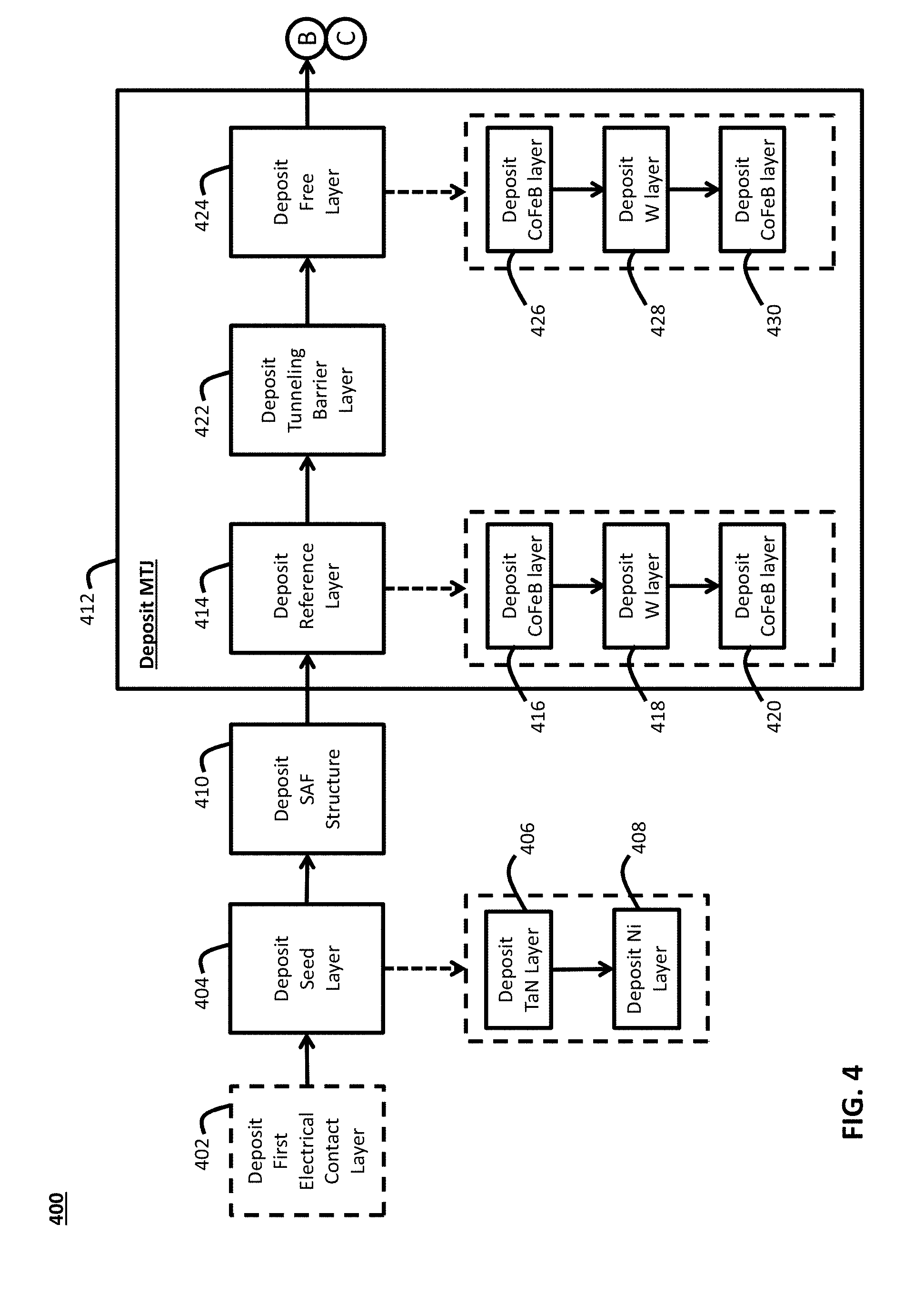
[0050] A flowchart showing a method 400 of manufacturing an embodiment of an MRAM stack, according to an embodiment, is illustrated in FIG. 4. The method 400 shown in FIG. 4 can be used to manufacture the MRAM stacks 200, 300 described in connection with FIGS. 2 and 3. Accordingly, to the extent that reference is made to MRAM stacks and the layers thereof, it is meant to be inclusive of the MTJ stacks 200, 300 of those figures and the other MTJ stacks described herein, and is not intended to be exclusive, even if reference is made to only one or a subset of the MTJ stacks in those figures.
[0051] The method 400 shown in FIG. 4 details how the MRAM stack is formed on a substrate, which in an embodiment can be a silicon substrate and in other embodiments can be any other appropriate substrate material. Optionally, at optional step 402, an optional first electrical contact layer 270, 370 may be deposited. The first electrical contact layer is made from electrically conductive material, such as Cu, Au, or another suitable conductor, and may be used as a bottom electrode to apply a voltage across the MTJ stack.
[0052] In step 404 seed layer 210, 310 is deposited. In an embodiment, the seed layer can be constructed by depositing, at step 406, a TaN layer and then, at step 408, depositing a Ni layer, which together form the seed layer. In an embodiment, the TaN layer is a thin film having a thickness of 5 nm and the Ni layer is a thin film having a thickness of 5 nm. In alternative embodiments, the TaN layer can have a thickness ranging from 2 nm to 20 nm while Ni layer can have a thickness ranging from 0 nm to 20 nm. According to an embodiment, the Ni layer can be replaced by a Cu layer or a layer made of other suitable materials.
[0053] At step 410, an SAF structure 220, 320 is deposited. As described herein, the SAF structure is a multi-layer structure that generally includes two or more thin magnetic layers having opposite or anti-parallel magnetization directions, which are separated by an antiferromagnetic coupling layer or spacer layer that is not magnetic. According to embodiments, the SAF structure is created in such a way to reduce stray magnetic fields by creating an imbalance in the total magnetic moment above and below the antiferromagnetic coupling layer. That imbalance can be created by adding auxiliary layers to the stack, or by adjusting the thickness and magnetic moment density of one or more layers of the SAF structure. U.S. patent application Ser. No. 15/634,629, referenced and incorporated by reference above, describes detailed methods for forming an SAF structure, including one or more auxiliary layers.
[0054] After deposition of the SAF structure in step 410, a magnetic tunnel junction ("MTJ") 230, 330 is deposited over the SAF structure in step 412. The MTJ includes multiple layers and is deposited in several steps, as shown in FIG. 4.
[0055] As part of the manufacture of the MTJ (step 412), in step 414, a reference layer 232, 332 is deposited. According to an embodiment, fabricating the reference layer includes several steps, including deposition of magnetic layer in step 416, deposition of a tungsten (W) layer in step 418, and deposition of another magnetic layer in step 420. In an embodiment, the magnetic layer deposited in step 416 comprises a thin film of CoFeB having a thickness of 0.6 nm, where the alloy is sixty (60) percent Fe, twenty (20) percent Co and twenty (20) percent B. In an embodiment, the W layer deposited in step 418 comprises a thin film of W having a thickness of 0.2 nm. In an embodiment, the magnetic layer deposited in step 420 comprises a thin film of CoFeB having a thickness of 0.8 nm, where the alloy is sixty (60) percent Fe, twenty (20) percent Co and twenty (20) percent B. In other embodiments, the magnetic layer deposited in step 416 can comprise a thin film of CoFeB having a thickness ranging from 0.5 nm to 1.0 nm, the W layer deposited in step 418 can comprise a thin film having a thickness of 0.1 nm to 1.0 nm, and the magnetic layer deposited in step 420 can comprise a thin film of CoFeB having a thickness of 0.5 nm to 2.0 nm. The reference layer of the MTJ is constructed using magnetic materials so that it has a magnetic vector having a magnetic direction perpendicular to its plane, is fixed in direction. According to an embodiment, the magnetic direction of the reference layer is antiparallel to the magnetic direction of the lower SAF1 layer of the SAF structure.
[0056] As part of the manufacture of the MTJ (step 412), at step 422, non-magnetic tunneling barrier layer 234, 334 is deposited on the reference layer. In an embodiment, the non-magnetic tunneling barrier is formed as a thin film of an insulating material, such as MgO.
[0057] The manufacture of the MTJ (step 412) continues at step 424, when a free layer 236, 336 is deposited over the non-magnetic tunneling barrier layer. According to an embodiment, the free layer is made from magnetic materials. Fabrication of free layer includes several steps. At step 426, a magnetic layer is deposited over non-magnetic tunneling barrier layer. In an embodiment, the magnetic layer deposited in step 426 is comprised of a thin film of CoFeB having a thickness of 1.2 nm, where the alloy is sixty (60) percent Fe, twenty (20) percent Co and twenty (20) percent B. In other embodiments, magnetic layer deposited in step 626 can comprise a thin film of CoFeB or other suitable magnetic material having a thickness ranging from 0.5 nm to 2.0 nm. Manufacture of free layer continues at step 428, where a Tungsten (W) layer is deposited over the magnetic layer deposited in step 426. In an embodiment, the W layer comprises a thin film of W having a thickness of 0.2 nm, and in other embodiments can a thickness ranging from 0.1 nm to 1.0 nm. At step 430, manufacture of the free layer continues when a second magnetic layer is deposited over the W layer deposited in step 428. In an embodiment, the second magnetic layer of the free layer deposited in step 430 can comprise a thin film of CoFeB having a thickness of 0.9 nm, where the alloy is sixty (60) percent Fe, twenty (20) percent Co and twenty (20) percent B. In other embodiments, the second magnetic layer deposited in step 430 can comprise a thin film of CoFeB or other suitable magnetic material having a thickness ranging from 0.5 nm to 1.5 nm.
[0058] Collectively, the first and second magnetic layers deposited in steps 426 and 430, along with non-magnetic W layer deposited in step 428, form the free layer formed in step 424. The free magnetic layer has a magnetic vector having a magnetic direction substantially perpendicular to its plane. Although the magnetic direction of the free magnetic layer is substantially perpendicular to its plane, it may also include magnetization pointing a few degrees away from the perpendicular axis. The tilted angle of the free layer magnetization can be due to interaction with a filter layer, such as a precessional spin current magnetic layer, described herein, or due to magneto crystalline anisotropy, and can help switching of the free layer magnetization by improving the initiation of the switching. The magnetic direction of the free layer can switch one hundred eighty (180) degrees from one direction to another, antiparallel, direction.
[0059] According to embodiments, including those shown and described in connection with FIG. 2, after fabrication of MTJ at step 412, process 400 is continued as process 500 in FIG. 5 at step 536. In step 536, a skyrmionic enhancement layer 260 is deposited over the free layer 236 of the MTJ 230. The skyrmionic enhancement layer 260 may be formed from heavy metals having a high atomic number and large spin-orbit coupling, such as W, Ir, Pt, Au, Pd, or suitable alloys thereof. The skyrmionic enhancement layer 260 may have a thickness in the range from 0.3 nm to 4 nm if formed from a single layer of metal, or in the range of 0.6 nm to 12 nm if formed from a multilayer. The skyrmionic enhancement layer 260 can be formed by a thin film sputter deposition system as would be appreciated by those skilled in such deposition techniques. The thin film sputter deposition system can include the necessary physical vapor deposition (PVD) chambers, each having one or more targets, an oxidation chamber, and a sputter etching chamber. Typically, the sputter deposition process involves a sputter gas (e.g., argon, krypton, xenon, or the like) with an ultra-high vacuum, and the targets can be made of the metal or metal alloys to be deposited on the free layer 236.
[0060] After deposition of the skyrmionic enhancement layer 260 in step 536, a hard mask layer is deposited in step 544. In step 548, a pillar is formed which may utilize various methods, including ion beam etching, followed by backfilling with insulating materials such as alumina (Al.sub.2O.sub.3), and then followed by chemical mechanical planarization.
[0061] After pillar formation in step 548 a second electrical contact layer 272 is deposited in step 550. The second electrical contact layer is made from electrically conductive material, such as Cu, Au, or another suitable conductor, and may be used as a top electrode to apply a voltage across the MTJ stack. The second electrical contact layer 272 may further be patterned by suitable subtractive methods, including ion beam etching, resulting in the formation of MTJ stack 200.
[0062] According to embodiments, including those shown and described in connection with FIG. 3, after fabrication of MTJ at step 412, process 400 is continued as process 600 in FIG. 6 at step 632. In step 632, a filter coupling layer 340 is deposited over the MTJ. In an embodiment, the spacer deposited in step 632 can comprise a thin film of MgO (as shown in step 634) having a thickness of 0.8 nm. In other embodiments, the spacer can comprise a thin film of MgO having a thickness ranging from 0.5 nm to 1.5 nm. In other embodiments, the spacer can be constructed as described in U.S. patent application Ser. No. 14/866,359, filed Sep. 25, 2015, and entitled "Spin Transfer Torque Structure For MRAM Devices Having A Spin Current Injection Capping Layer." U.S. patent application Ser. No. 14/866,359 is hereby incorporated by reference in its entirety.
[0063] After deposition of spacer layer in step 632, a precessional spin current layer 350 is deposited in step 636. As shown in FIG. 6, the manufacture of the precessional spin current layer can comprise several steps. At step 638, a magnetic Fe layer is fabricated over the filter coupling layer deposited in step 632. In an embodiment, the magnetic Fe layer comprises a thin film of Fe having a thickness of 0.6 nm. In other embodiments, magnetic Fe layer deposited in step 638 can comprise a thin film of Fe having a thickness ranging from 0.5 nm to 2.0 nm. At step 640, a Ru layer is deposited over the magnetic Fe layer. In an embodiment, Ru layer deposited in step 640 can comprise a thin film of Ru having a thickness of 1.5 nm, and in other embodiments can comprise a thin film of Ru having a thickness ranging from 0.4 nm to 5.0 nm. At step 642, a magnetic NiFe layer is deposited. In an embodiment, magnetic NiFe layer comprises eighty (80) percent Ni and twenty (20) percent Fe, and has a thickness of 3.0 nm. In other embodiments, the NiFe layer can have a thickness ranging between 0.5 nm to 7.0 nm. NiFe layer can also comprise multiple layers, such as a thin film of CoFeB and NiFe according to an embodiment, or a NiFe layer in between layers of CoFeB, according to another embodiment.
[0064] In step 643, a skyrmionic enhancement layer 360 is deposited over the precessional spin current layer 350. The skyrmionic enhancement layer 360 may be formed from heavy metals having a high atomic number and large spin-orbit coupling, such as W, Ir, Pt, Au, Pd, or suitable alloys thereof. The skyrmionic enhancement layer 360 may have a thickness in the range from 1 nm to 4 nm if formed from a single layer of metal, or in the range of 0.6 nm to 12 nm if formed from a multilayer The skyrmionic enhancement layer 360 can be formed by a thin film sputter deposition system as would be appreciated by those skilled in such deposition techniques. The thin film sputter deposition system can include the necessary physical vapor deposition (PVD) chambers, each having one or more targets, an oxidation chamber, and a sputter etching chamber. Typically, the sputter deposition process involves a sputter gas (e.g., argon, krypton, xenon, or the like) with an ultra-high vacuum, and the targets can be made of the metal or metal alloys to be deposited on the precessional spin current layer 350.
[0065] After deposition of skyrmionic enhancement layer 360 in step 643, a hard mask layer is deposited in step 644. In step 648, a pillar is formed which may utilize various methods, including ion beam etching, followed by backfilling with insulating materials such as alumina (Al.sub.2O.sub.3), and then followed by chemical mechanical planarization.
[0066] After pillar formation in step 648 a second electrical contact layer 372 is deposited in step 650. The second electrical contact layer is made from electrically conductive material, such as Cu, Au, or another suitable conductor, and may be used a top electrode to apply a voltage across the MTJ stack. The second electrical contact layer 372 may further be patterned by suitable subtractive methods, including ion beam etching, resulting in the formation of MTJ stack 300.
[0067] All of the layers of the MRAM devices 200, 300 illustrated in FIGS. 2 and 3 can be formed by a thin film sputter deposition system as would be appreciated by those skilled in such deposition techniques. The thin film sputter deposition system can include the necessary physical vapor deposition (PVD) chambers, each having one or more targets, an oxidation chamber and a sputter etching chamber. Typically, the sputter deposition process involves a sputter gas (e.g., argon, krypton, xenon, or the like) with an ultra-high vacuum and the targets can be made of the metal or metal alloys to be deposited on the substrate. Thus, when the present specification states that a layer is placed over another layer, such layer could have been deposited using such a system. Other methods can be used as well. It should be appreciated that the remaining steps necessary to manufacture MTJ stacks 200, 300 are well-known to those skilled in the art and will not be described in detail herein so as not to unnecessarily obscure aspects of the disclosure herein.
[0068] It should be appreciated to one skilled in the art that a plurality of MTJ structures 200, 300 can be manufactured and provided as respective bit cells of an STT-MRAM device. In other words, each MTJ stack 200, 300 can be implemented as a bit cell for a memory array having a plurality of bit cells.
[0069] It should be recognized that certain components or elements of the embodiments described above, or in the claims that follow, are numbered to allow ease of reference to them or to help distinguish between them, but order should not be implied from such numbering, unless such order is expressly recited. The above description and drawings are only to be considered illustrative of specific embodiments, which achieve the features and advantages described herein. Modifications and substitutions to specific process conditions can be made. Accordingly, the embodiments in this patent document are not considered as being limited by the foregoing description and drawings.
* * * * *
D00000
D00001
D00002
D00003
D00004
D00005
D00006
XML
uspto.report is an independent third-party trademark research tool that is not affiliated, endorsed, or sponsored by the United States Patent and Trademark Office (USPTO) or any other governmental organization. The information provided by uspto.report is based on publicly available data at the time of writing and is intended for informational purposes only.
While we strive to provide accurate and up-to-date information, we do not guarantee the accuracy, completeness, reliability, or suitability of the information displayed on this site. The use of this site is at your own risk. Any reliance you place on such information is therefore strictly at your own risk.
All official trademark data, including owner information, should be verified by visiting the official USPTO website at www.uspto.gov. This site is not intended to replace professional legal advice and should not be used as a substitute for consulting with a legal professional who is knowledgeable about trademark law.