Compound Semiconductor Device
SASAKI; Kenji ; et al.
U.S. patent application number 16/355172 was filed with the patent office on 2019-07-11 for compound semiconductor device. This patent application is currently assigned to Murata Manufacturing Co., Ltd.. The applicant listed for this patent is Murata Manufacturing Co., Ltd.. Invention is credited to Takashi KITAHARA, Kingo KUROTANI, Kenji SASAKI.
| Application Number | 20190214489 16/355172 |
| Document ID | / |
| Family ID | 56079674 |
| Filed Date | 2019-07-11 |


View All Diagrams
| United States Patent Application | 20190214489 |
| Kind Code | A1 |
| SASAKI; Kenji ; et al. | July 11, 2019 |
COMPOUND SEMICONDUCTOR DEVICE
Abstract
A compound semiconductor device includes a heterojunction bipolar transistor and a bump. The heterojunction bipolar transistor includes a plurality of unit transistors. The bump is electrically connected to emitters of the plurality of unit transistors. The plurality of unit transistors are arranged in a first direction. The bump is disposed above the emitters of the plurality of unit transistors while extending in the first direction. The emitter of at least one of the plurality of unit transistors is displaced from a center line of the bump in the first direction toward a first side of a second direction which is perpendicular to the first direction. The emitter of at least another one of the plurality of unit transistors is displaced from the center line of the bump in the first direction toward a second side of the second direction.
| Inventors: | SASAKI; Kenji; (Nagaokakyo-shi, JP) ; KUROTANI; Kingo; (Nagaokakyo-shi, JP) ; KITAHARA; Takashi; (Nagaokakyo-shi, JP) | ||||||||||
| Applicant: |
|
||||||||||
|---|---|---|---|---|---|---|---|---|---|---|---|
| Assignee: | Murata Manufacturing Co.,
Ltd. Kyoto-fu JP |
||||||||||
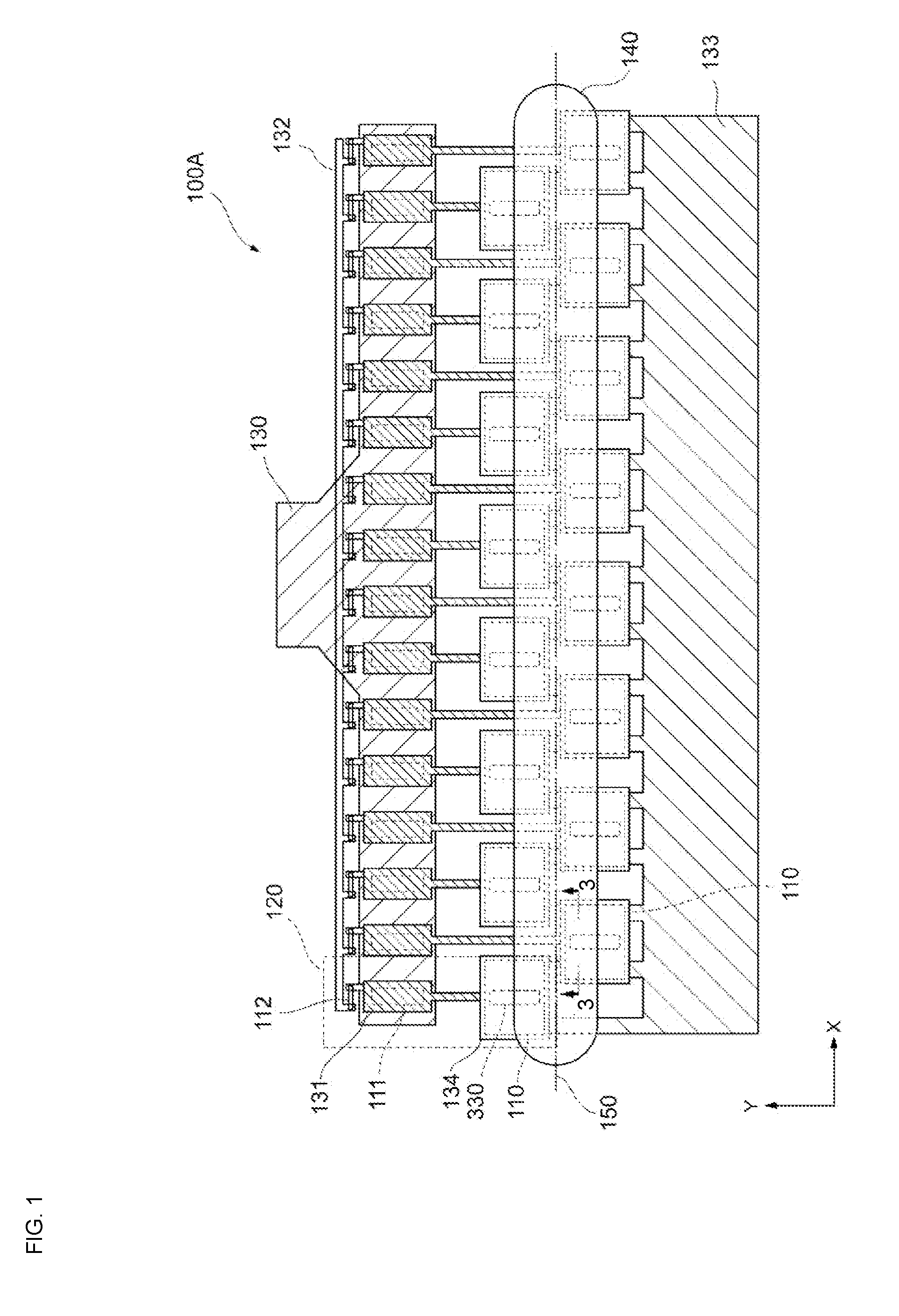
| Family ID: | 56079674 | ||||||||||
| Appl. No.: | 16/355172 | ||||||||||
| Filed: | March 15, 2019 |
Related U.S. Patent Documents
| Application Number | Filing Date | Patent Number | ||
|---|---|---|---|---|
| 15709017 | Sep 19, 2017 | 10276701 | ||
| 16355172 | ||||
| 14932497 | Nov 4, 2015 | 9825156 | ||
| 15709017 | ||||
| Current U.S. Class: | 1/1 |
| Current CPC Class: | H01L 29/40 20130101; H01L 29/0692 20130101; H01L 24/16 20130101; H01L 24/13 20130101; H01L 29/41708 20130101; H01L 2224/1302 20130101; H01L 2924/13051 20130101; H01L 23/4824 20130101; H01L 23/535 20130101; H01L 24/05 20130101; H03F 2200/408 20130101; H01L 2224/0401 20130101; H01L 2224/13013 20130101; H01L 27/0823 20130101; H01L 29/7371 20130101; H03F 2200/451 20130101; H01L 2224/16227 20130101; H03F 3/19 20130101; H01L 2224/1302 20130101; H01L 2924/00012 20130101; H01L 2224/13013 20130101; H01L 2924/00012 20130101 |
| International Class: | H01L 29/737 20060101 H01L029/737; H03F 3/19 20060101 H03F003/19; H01L 23/535 20060101 H01L023/535; H01L 29/417 20060101 H01L029/417; H01L 29/06 20060101 H01L029/06; H01L 27/082 20060101 H01L027/082; H01L 23/00 20060101 H01L023/00; H01L 23/482 20060101 H01L023/482; H01L 29/40 20060101 H01L029/40 |
Foreign Application Data
| Date | Code | Application Number |
|---|---|---|
| Nov 27, 2014 | JP | 2014-240327 |
Claims
1. A compound semiconductor device comprising: a heterojunction bipolar transistor including a plurality of unit transistors; a metal-insulator-metal capacitor electrically connected between a RF input wire and a base wire for each unit transistor of the plurality of unit transistors; and a bump electrically connected to emitters of the plurality of unit transistors, wherein the plurality of unit transistors are arranged in a first direction, the bump is disposed above the emitters of the plurality of unit transistors while extending in the first direction, and the bump is partially disposed above the base wire.
2. A compound semiconductor device according to claim 1, wherein the plurality of unit transistors include a first unit transistor and a second unit transistor, the emitter of the first unit transistor being disposed on a first side of a second direction with respect to a center line of the bump extending in the first direction, the emitter of the second unit transistor being disposed on a second side of the second direction with respect to the center line of the bump, the second direction being perpendicular to the first direction, no portion of any emitter of the first unit transistor is disposed on the second side and no portion of any emitter of the second unit transistor is disposed on the first side, and the emitter of the first unit transistor is offset in the first direction and in the second direction with respect to the emitter of the second unit transistor.
3. A compound semiconductor device according to claim 2, wherein each unit transistor has a resistor connected at one end to a bias control wire and at the other end to the base wire.
4. A compound semiconductor device according to claim 3, wherein each of the resistor is not covered by the bump.
5. A compound semiconductor device according to claim 4, wherein the emitters of the plurality of unit transistors are displaced from the center line of the bump toward the first side and second side alternately by one by one.
6. A compound semiconductor device according to claim 4, wherein the emitters of the plurality of unit transistors are displaced from the center line of the bump toward the first side and second side alternately by a group of a plurality of unit transistors.
7. A power amplifier module comprising: the compound semiconductor device according to claim 2, wherein, the bumps are connected to a ground surface of module substrates.
8. A power amplifier module comprising: the compound semiconductor device according to claim 3, wherein, the bumps are connected to a ground surface of module substrates.
9. A power amplifier module comprising: the compound semiconductor device according to claim 4, wherein, the bumps are connected to a ground surface of module substrates.
10. A power amplifier module comprising: the compound semiconductor device according to claim 5, wherein, the bumps are connected to a ground surface of module substrates.
11. A power amplifier module comprising: the compound semiconductor device according to claim 6, wherein, the bumps are connected to a ground surface of module substrates.
12. A compound semiconductor device having sub-groups and each sub-group comprising: a heterojunction bipolar transistor including a plurality of unit transistors; a metal-insulator-metal capacitor electrically connected between a RF input wire and a base wire for each unit transistor of the plurality of unit transistors; and a bump electrically connected to emitters of the plurality of unit transistors, wherein the plurality of unit transistors are arranged in a first direction, the bump is disposed above the emitters of the plurality of unit transistors while extending in the first direction, and the bump is partially disposed above the base wire.
13. A compound semiconductor device according to claim 12, wherein the plurality of unit transistors include a first unit transistor and a second unit transistor, the emitter of the first unit transistor being disposed on a first side of a second direction with respect to a center line of the bump extending in the first direction, the emitter of the second unit transistor being disposed on a second side of the second direction with respect to the center line of the bump, the second direction being perpendicular to the first direction, no portion of any emitter of the first unit transistor is disposed on the second side and no portion of any emitter of the second unit transistor is disposed on the first side, and the emitter of the first unit transistor is offset in the first direction and in the second direction with respect to the emitter of the second unit transistor.
14. A compound semiconductor device according to claim 13, wherein each unit transistor has a resistor connected at one end to a bias control wire and at the other end to the base wire.
15. A compound semiconductor device according to claim 14, wherein each of the resistor is not covered by the bump.
16. A compound semiconductor device according to claim 15, wherein the emitters of the plurality of unit transistors are displaced from the center line of the bump toward the first side and second side alternately by one by one.
17. A compound semiconductor device according to claim 15, wherein the emitters of the plurality of unit transistors are displaced from the center line of the bump toward the first side and second side alternately by a group of a plurality of unit transistors.
18. A power amplifier module comprising: the compound semiconductor device according to claim 13, wherein, the bumps are connected to a ground surface of module substrates.
19. A power amplifier module comprising: the compound semiconductor device according to claim 14, wherein, the bumps are connected to a ground surface of module substrates.
20. A power amplifier module comprising: the compound semiconductor device according to claim 15, wherein, the bumps are connected to a ground surface of module substrates.
21. A power amplifier module comprising: the compound semiconductor device according to claim 16, wherein, the bumps are connected to a ground surface of module substrates.
22. A power amplifier module comprising: the compound semiconductor device according to claim 17, wherein, the bumps are connected to a ground surface of module substrates.
Description
CROSS REFERENCE TO RELATED APPLICATIONS
[0001] This Application is a Continuation of U.S. patent application Ser. No. 15/709,017 filed on Sep. 19, 2017, which is a Continuation of U.S. patent application Ser. No. 14/932,497 filed on Nov. 4, 2015, which claims benefit of priority to Japanese Patent Application No. 2014-240327 filed on Nov. 27, 2014, the entire content of which is incorporated herein by reference.
TECHNICAL FIELD
[0002] The present disclosure relates to a compound semiconductor device and a power amplifier module.
BACKGROUND
[0003] In a mobile communication device, such as a cellular phone, a power amplifier module is used for amplifying power of a radio-frequency (RF) signal to be transmitted to a base station. In a power amplifier module, a compound semiconductor device including a heterojunction bipolar transistor (HBT) as an amplifier element is used.
[0004] In accordance with smaller sizes of recent mobile communication devices, it is also desirable to reduce the size of compound semiconductor devices. In order to satisfy this demand, as disclosed in Japanese Unexamined Patent Application Publication No. 2000-106386, for example, flip-chip mounting may be used instead of wire bonding as a technique for mounting a compound semiconductor device on a module substrate.
SUMMARY
[0005] In the configuration disclosed in the above-described publication, a plurality of unit transistors are linearly arranged, and a bump is provided over the emitters of the unit transistors. With this configuration, the emitters, which are heat sources, are disposed close to each other. This may increase the thermal resistance.
[0006] The present disclosure has been made in view of the above-described background. It is an object of the present disclosure to reduce the thermal resistance in a compound semiconductor device including an HBT constituted by a plurality of unit transistors.
[0007] According to a preferred embodiment of the present disclosure, there is provided a compound semiconductor device including a heterojunction bipolar transistor and a bump. The heterojunction bipolar transistor includes a plurality of unit transistors. The bump is electrically connected to emitters of the plurality of unit transistors. The plurality of unit transistors are arranged in a first direction. The bump is disposed above the emitters of the plurality of unit transistors while extending in the first direction. The emitter of at least one of the plurality of unit transistors is displaced from a center line of the bump in the first direction toward a first side of a second direction which is perpendicular to the first direction. The emitter of at least another one of the plurality of unit transistors is displaced from the center line of the bump in the first direction toward a second side of the second direction.
[0008] According to a preferred embodiment of the present disclosure, it is possible to reduce the thermal resistance in a compound semiconductor device including an HBT constituted by a plurality of unit transistors.
[0009] Other features, elements, characteristics and advantages of the present disclosure will become more apparent from the following detailed description of preferred embodiments of the present disclosure with reference to the attached drawings.
BRIEF DESCRIPTION OF THE DRAWINGS
[0010] FIG. 1 is a plan view of a compound semiconductor device according to an embodiment of the disclosure.
[0011] FIG. 2 is a circuit diagram of a cell forming the compound semiconductor device shown in FIG. 1.
[0012] FIG. 3 is a sectional view of the compound semiconductor device taken along line 3-3 of FIG. 1.
[0013] FIG. 4 illustrates an example in which the compound semiconductor device is flip-chip mounted.
[0014] FIG. 5A illustrates an example in which emitters are linearly arranged on the center line of a bump (linear arrangement).
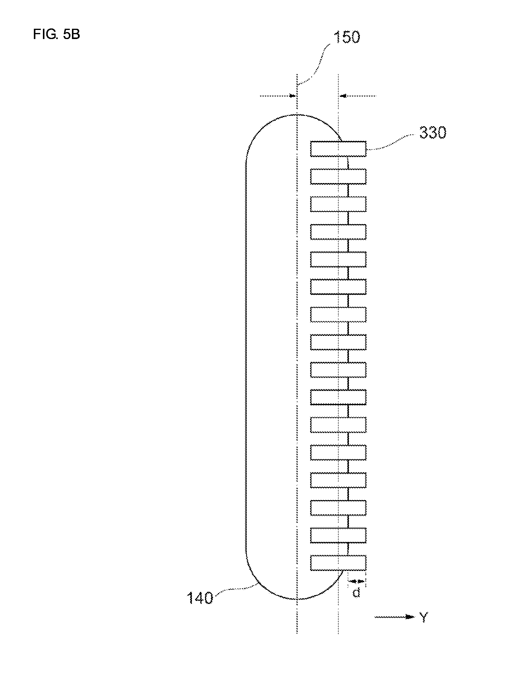
[0015] FIG. 5B illustrates an example in which emitters are displaced from the center line of a bump toward one side (+Y side) (linear arrangement).
[0016] FIG. 5C illustrates an example in which emitters are displaced from the center line of a bump alternately toward one side (+Y side) and the other side (-Y side).
[0017] FIG. 6 is a graph illustrating simulation results indicating how the thermal resistance changes according to the amount by which emitters are displaced from the center line of a bump.
[0018] FIG. 7 is a plan view of a compound semiconductor device according to another embodiment of the disclosure.
[0019] FIG. 8 is a plan view of a compound semiconductor device according to another embodiment of the disclosure.
[0020] FIG. 9 is a plan view of a compound semiconductor device according to another embodiment of the disclosure.
[0021] FIG. 10 illustrates the configuration of a power amplifier module according to an embodiment of the disclosure.
DETAILED DESCRIPTION
[0022] FIG. 1 is a plan view of a compound semiconductor device 100A according to an embodiment of the disclosure. FIG. 2 is a circuit diagram of a cell forming the compound semiconductor device 100A. FIG. 3 is a sectional view of the compound semiconductor device 100A taken along line 3-3 of FIG. 1. FIG. 4 illustrates an example in which the compound semiconductor device 100A is flip-chip mounted. An example of the configuration of the compound semiconductor device 100A will be described below with reference to FIGS. 1 through 4.
[0023] As shown in FIG. 1, the compound semiconductor device 100A includes a plurality of unit transistors 110. These unit transistors 110 form an HBT. The unit transistors 110 are also called "fingers". In the example shown in FIG. 1, sixteen unit transistors 110 form an HBT. That is, the number of fingers of the HBT is sixteen. However, the number of fingers of the HBT is not restricted to sixteen.
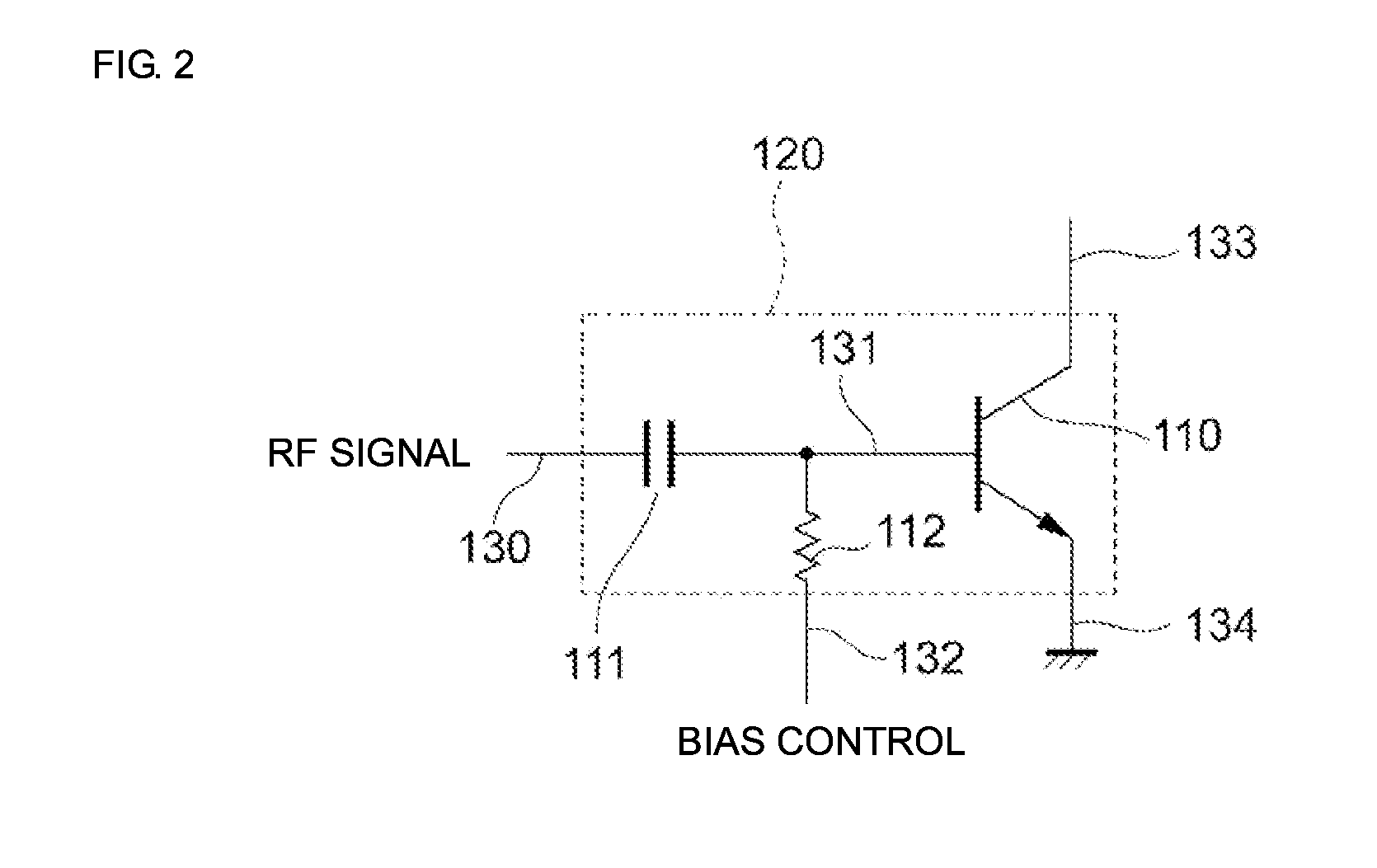
[0024] Each unit transistor 110 forms a cell 120, together with a capacitor 111 and a resistor 112. The circuit diagram of the cell 120 is shown in FIG. 2. Each cell 120 amplifies an input RF signal and outputs an amplified RF signal from the collector of the unit transistor 110. A plurality of cells 120 are connected in parallel with each other and form an amplifier which amplifies an RF signal.
[0025] The capacitor 111 is formed between an RF input wire 130 into which an RF signal is input and a base wire 131 connected to the base of the unit transistor 110. The capacitor 111 may be formed as a metal-insulator-metal (MIM) capacitor between the RF input wire 130 and the base wire 131. The capacitor 111 blocks DC components of an RF signal and outputs the RF signal.
[0026] The resistor 112 is connected at one end to a bias control wire 132 and at the other end to the base wire 131. Bias is applied to the base of the unit transistor 110 via this resistor 112.
[0027] The base of the unit transistor 110 is connected to the base wire 131. The collector of the unit transistor 110 is connected to a collector wire 133. The emitter of the unit transistor 110 is connected to an emitter wire 134. As shown in FIG. 1, the emitter wire 134 is connected to a bump 140. The bump 140 is grounded, so that the emitter of the unit transistor 110 is also grounded.
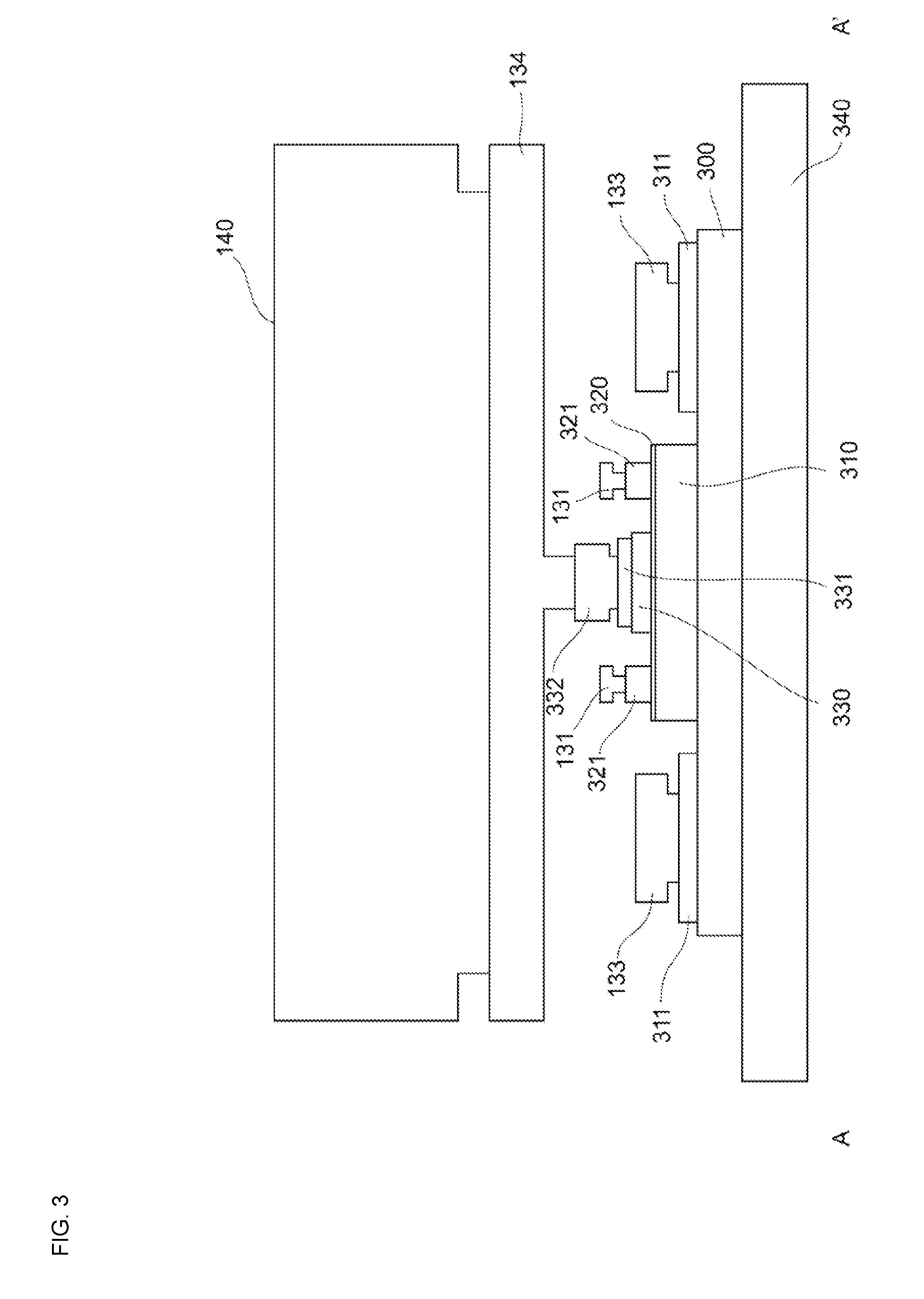
[0028] The sectional structure of the unit transistor 110 will be discussed below with reference to FIG. 3. The unit transistor 110 includes a sub-collector 300, a collector 310, a collector electrode 311, a base 320, a base electrode 321, an emitter 330, and an emitter electrode 331.
[0029] The sub-collector 300 is formed on, for example, a gallium arsenide (GaAs) substrate 340. The collector 310 and the collector electrode 311 are formed on the sub-collector 300. The base 320 is formed on the collector 310. The base electrode 321 is formed on the base 320.
[0030] As shown in FIG. 3, the collector 310 is electrically connected to the collector wire 133 via the sub-collector 300 and the collector electrode 311. The base 320 is electrically connected to the base wire 131 via the base electrode 321. The emitter 330 is electrically connected to the bump 140 via the emitter electrode 331 and emitter wires 134 and 332. As shown in FIG. 3, the bump 140 is formed above the emitter 330.
[0031] As shown in FIG. 4, the compound semiconductor device 100A is mounted on a module substrate 410, together with a surface mount device (SMD) 400, for example. The compound semiconductor device 100A is mounted on the module substrate 410 with the bump 140 facing down the module substrate 410. The bump 140 is connected to a ground surface 420.
[0032] The positional relationship between the unit transistors 110 and the bump 140 in the compound semiconductor device 100A will be discussed below. As shown in FIG. 1, the multiple unit transistors 110 are arranged in the X-axis direction (first direction) shown in FIG. 1. The bump 140 is formed over the emitters 330 of the multiple unit transistors 110 and extends in the X-axis direction. As viewed from the bump 140, the emitter 330 of each unit transistor 110 is at least partially covered by the bump 140. The emitters 330 of the multiple unit transistors 110 are displaced from a center line 150 of the bump 140 alternately toward one side (first side), for example, the +Y side, and the other side (second side), for example, the -Y side, in the Y-axis direction (second direction) shown in FIG. 1.
[0033] With this arrangement, the positions of heat sources (emitters 330) can be distributed more separately than a case in which the emitters 330 of all the unit transistors 110 are linearly arranged along the center line 150 of the bump 140. This makes it possible to reduce the thermal resistance in the compound semiconductor device 100A.
[0034] As shown in FIG. 1, in the compound semiconductor device 100A, part of the emitter 330 of each unit transistor 110 is not covered by the bump 140. With this configuration, stress to be applied to the emitters 330 can be reduced compared with a case in which the emitters 330 are entirely covered by the bump 140, thereby making it possible to prolong the life of the unit transistors 110.
[0035] A description will now be given below, with reference to FIGS. 5A through 6, how the thermal resistance changes according to the positional relationship between the bump 140 and the emitters 330.
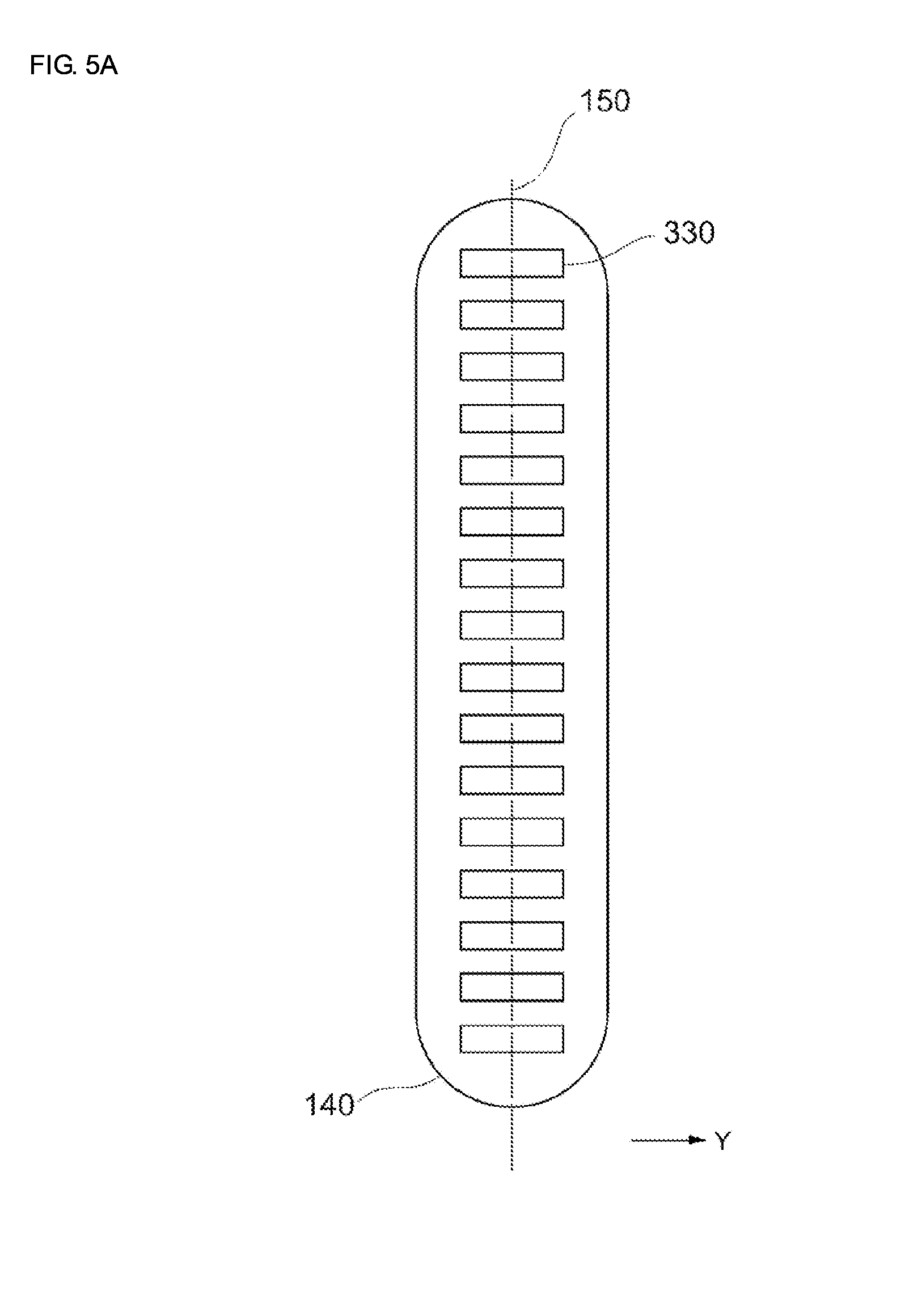
[0036] FIG. 5A illustrates an example in which the emitters 330 are linearly arranged on the center line 150 of the bump 140 (linear arrangement). FIG. 5B illustrates an example in which the emitters 330 are displaced from the center line 150 of the bump 140 toward one side (+Y side) (linear arrangement). FIG. 5C illustrates an example in which the emitters 330 are displaced from the center line 150 of the bump 140 alternately toward one side (+Y side) and the other side (-Y side), as in the compound semiconductor device 100A.
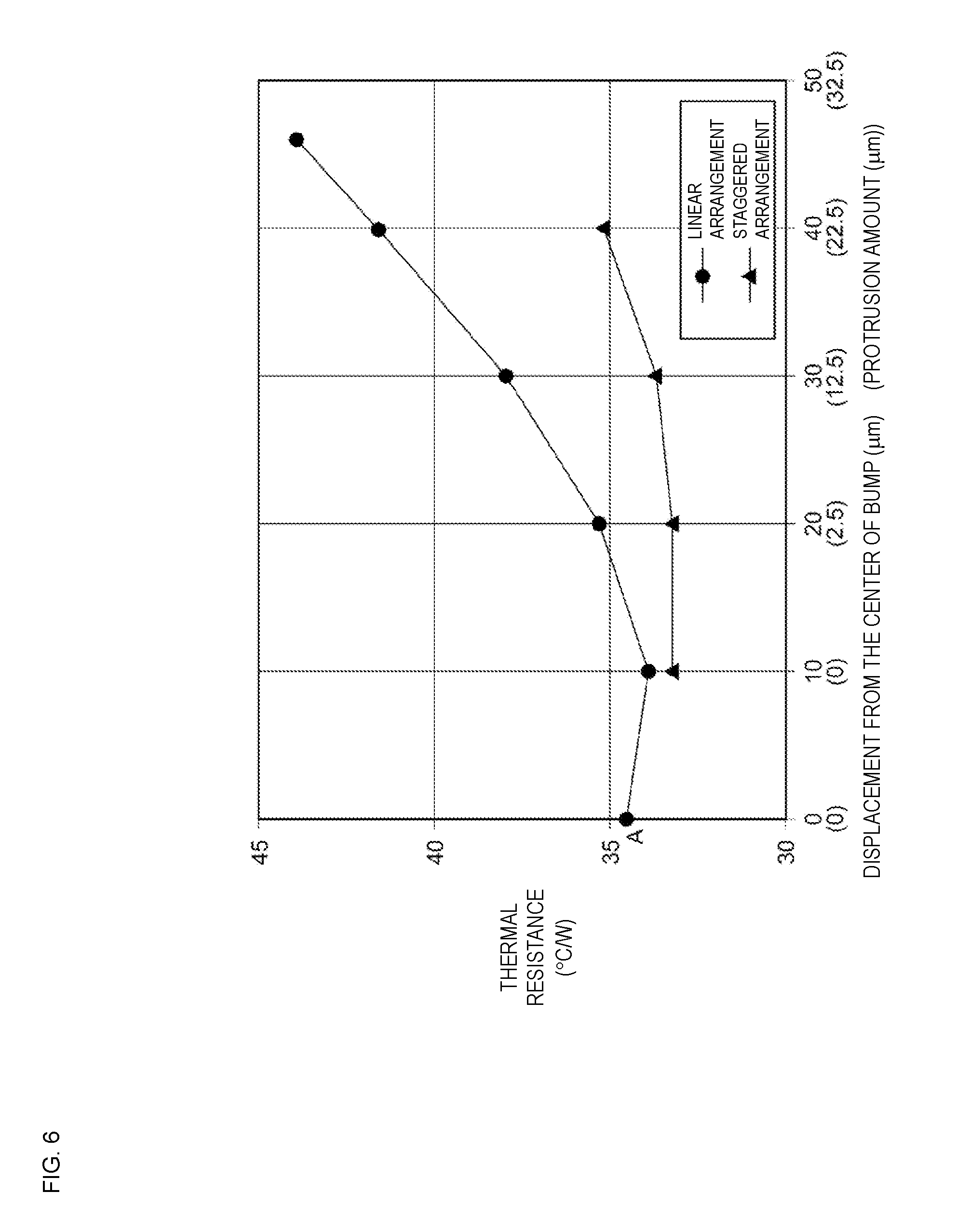
[0037] FIG. 6 is a graph illustrating simulation results indicating how the thermal resistance changes according to the amount by which the emitters 330 are displaced from the center line 150 of the bump 140 (hereinafter such an amount will simply be called a displacement). In FIG. 6, the horizontal axis indicates the displacement (distance) (.mu.m) between the center of the emitter 330 and the center line 150 of the bump 140, while the vertical axis indicates the thermal resistance (.degree. C./W). In FIG. 6, the line represented by the solid circles (linear arrangement) corresponds to the arrangements shown in FIGS. 5A and 5B, and the line represented by the solid triangles (staggered arrangement) corresponds to the arrangement shown in FIG. 5C.
[0038] The simulations were carried out under the following conditions: the dimension of the bump 140 in the Y-axis direction was about 75 .mu.m, and the dimension of the emitters 330 in the Y-axis direction was about 40 .mu.m; and the displacement of the emitters 330 was varied to about 0 .mu.m, 10 .mu.m, 20 .mu.m, 30 .mu.m, 40 .mu.m, and 50 .mu.m.
[0039] When the displacement of the emitters 330 is about 0 .mu.m, 10 .mu.m, 20 .mu.m, 30 .mu.m, 40 .mu.m, and 50 .mu.m, the amount by which the emitters 330 protrude from the edge of the bump 140 (protrusion amount d) is about 0 .mu.m, 0 .mu.m, 2.5 .mu.m, 12.5 .mu.m, 22.5 .mu.m, and 32.5 .mu.m, respectively.
[0040] As shown in FIG. 6, in the case of the linear arrangement, when the displacement of the emitters 330 is increased, as in FIG. 5B, to about 10 .mu.m, the thermal resistance becomes slightly smaller than that in a case in which the emitters 330 are not displaced at all (point A in FIG. 6). However, as the displacement of the emitters 330 is further increased, the thermal resistance becomes higher.
[0041] In contrast, as shown in FIG. 6, in the case of the staggered arrangement, when the displacement of the emitters 330 is about 10 .mu.m, 20 .mu.m, and 30 .mu.m, the thermal resistance is smaller than that in a case in which the emitters 330 are not displaced at all (point A in FIG. 6).
[0042] The above-described simulation results show that, by displacing the emitters 330 from the center line 150 of the bump 140 toward one side (+Y side) and the other side (-Y side), it is possible to reduce the thermal resistance to a smaller level than that in a case in which the emitters 330 are not displaced at all (point A).
[0043] The above-described simulation results also show that, in the case of the staggered arrangement, when the protrusion amount d of the emitters 330 is about 2.5 .mu.m (displacement of 20 .mu.m) and about 12.5 .mu.m (displacement of 30 .mu.m), it is possible to reduce the thermal resistance to a smaller level than that in a case in which the emitters 330 are not displaced at all (point A). That is, in the case of the staggered arrangement, when part of the emitter 330 of each unit transistor 110 is not covered by the bump 140, a decrease in the thermal resistance is also implemented. In this configuration, stress to be applied to the emitters 330 is reduced compared with a case in which the emitters 330 are entirely covered by the bump 140, thereby making it possible to prolong the life of the unit transistors 110.
[0044] Modified examples of the compound semiconductor device 100A will now be described below. In the following modified examples, the same elements as those of the compound semiconductor device 100A are designated by like reference numerals, and an explanation thereof will thus be omitted.
[0045] FIG. 7 is a plan view of a compound semiconductor device 100B according to an embodiment of the disclosure. In the compound semiconductor device 100B, a plurality of unit transistors 110 are grouped into multiple blocks, and a bump 140 is provided for each block. More specifically, eight unit transistors 110 form a block 700 and the other eight unit transistors form another block 710.
[0046] FIG. 8 is a plan view of a compound semiconductor device 100C according to an embodiment of the disclosure. In the compound semiconductor device 100C, as well as the compound semiconductor device 100B, a plurality of unit transistors 110 are grouped into multiple blocks, and a bump 140 is provided for each block. More specifically, four unit transistors 110 form each of blocks 800, 810, 820, and 830.
[0047] FIG. 9 is a plan view of a compound semiconductor device 100D according to an embodiment of the disclosure. In the compound semiconductor device 100D, a plurality of unit transistors 110 are displaced from the center line of the bump alternately by the group of two unit transistors 110. In this manner, instead of being displaced alternately one by one, the emitters 330 of the unit transistors 110 may be displaced alternately by the group of multiple unit transistors 110. In the example shown in FIG. 9, two unit transistors 110 are formed into each group, but three or more unit transistors 110 may be formed into each group.
[0048] In the configurations of the compound semiconductor devices 100B through 100D shown in FIGS. 7 through 9, by displacing the emitters 330 of the unit transistors 110 from the center line 150 of the bump 140, it is possible to reduce the thermal resistance, as in the compound semiconductor device 100A.
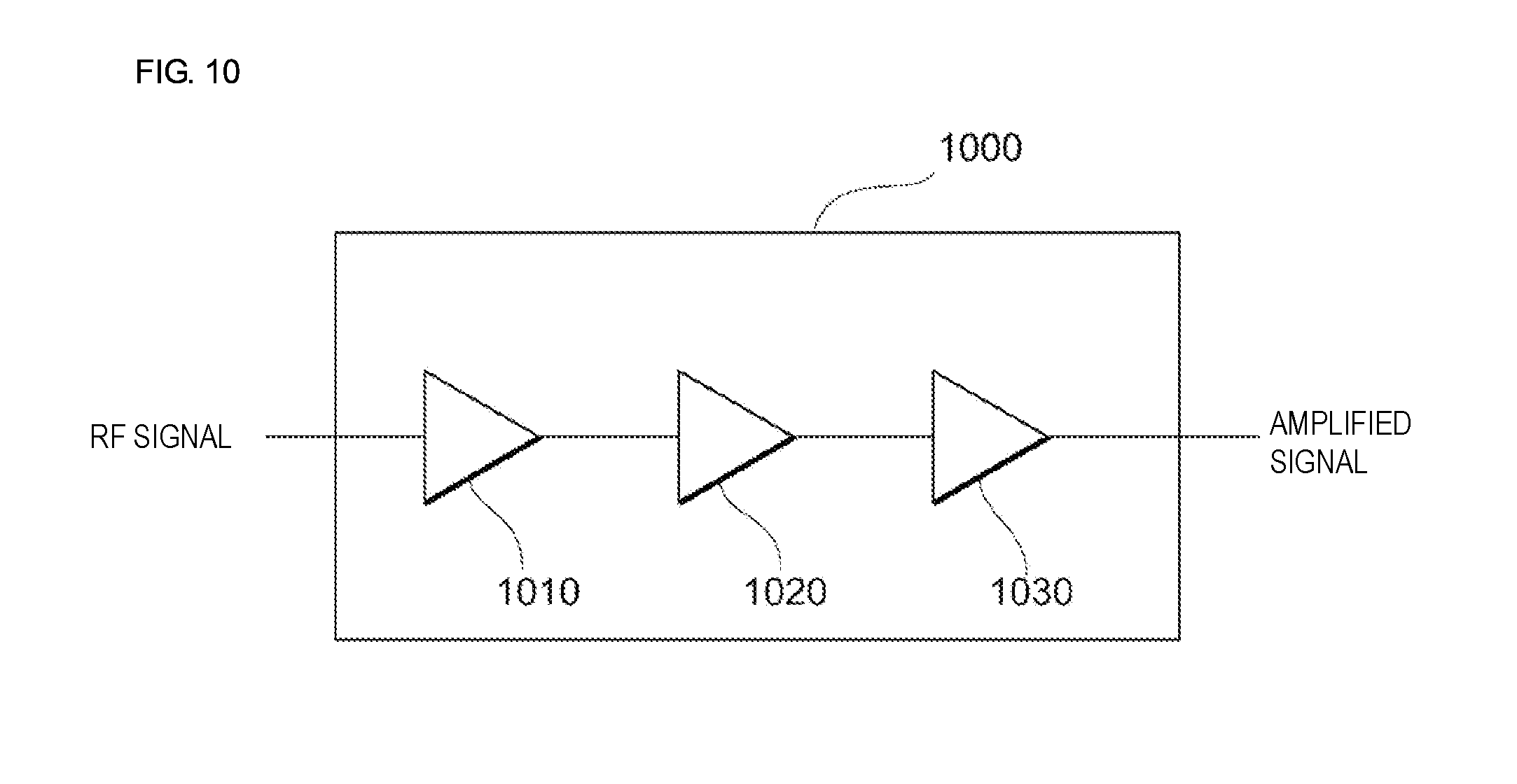
[0049] FIG. 10 illustrates the configuration of a power amplifier module 1000 according to an embodiment of the disclosure. The power amplifier module 1000 includes three stages of amplifiers 1010, 1020, and 1030. Each of the amplifiers 1010, 1020, and 1030 amplifies an input RF signal and outputs the amplified RF signal. In the power amplifier module 1000, the compound semiconductor device 100A is used in, for example, the amplifier 1030 at the final stage, thereby making it possible to reduce the thermal resistance in the amplifier 1030. The compound semiconductor device 100A may be used in the amplifier 1010 or 1020. However, since the current flowing through the amplifier 1030 at the final stage is greater, the effect of reducing the thermal resistance is enhanced if the compound semiconductor device 100A is used in the amplifier 1030. Instead of using the compound semiconductor device 100A, another compound semiconductor device 100B, 100C, or 100D may be used in the power amplifier module 1000.
[0050] The present disclosure has been described through illustration of preferred embodiments. According to the preferred embodiments, the emitter 330 of at least one of multiple unit transistors 110 is arranged such that it is displaced from the center line 150 of the bump 140 toward one side (first side), for example, the +Y side, and at least another one of the multiple unit transistors 110 is arranged such that it is displaced from the center line 150 of the bump 140 toward another side (second side), for example, the -Y side.
[0051] With this configuration, the positions of heat sources can be distributed more separately than the configuration in which the emitters 330 of all the unit transistors 110 are aligned along the center line 150 of the bump 140. Thus, in the compound semiconductor devices 100A through 100D, it is possible to reduce the thermal resistance to a smaller level than that in a case in which the emitters 330 of all the unit transistors 110 are aligned along the center line 150 of the bump 140.
[0052] In the compound semiconductor devices 100A through 100D, all the unit transistors 110 are displaced from the center line 150 of the bump 140. However, some unit transistors 110 may be disposed on the center line 150.
[0053] According to the preferred embodiments, the emitters 330 displaced from the center line 150 of the bump 140 may be partially exposed from the bump 140. With this configuration, stress to be applied to the emitters 330 can be reduced compared with a case in which the emitters 330 are entirely covered by the bump 140, thereby making it possible to prolong the life of the unit transistors 110.
[0054] According to the preferred embodiments, as in the compound semiconductor devices 100A, 100B, and 100C, the emitters 330 of the multiple unit transistors 110 may be displaced from the center line 150 of the bump 140 alternately toward one side (for example, the +Y side) and the other side (for example, the -Y side). With this configuration, it is possible to reduce the thermal resistance to a smaller level than that in a case in which the emitters 330 of all the unit transistors 110 are aligned along the center line 150 of the bump 140.
[0055] According to the preferred embodiments, as in the compound semiconductor device 100D, the emitters 330 of the multiple unit transistors 110 may be displaced from the center line 150 of the bump 140 toward one side (for example, the +Y side) and the other side (for example, the -Y side) alternately by the group of multiple unit transistors 110. With this configuration, it is also possible to reduce the thermal resistance to a smaller level than a case in which the emitters 330 of all the unit transistors 110 are aligned along the center line 150 of the bump 140.
[0056] According to the preferred embodiments, a power amplifier module may be formed by using the HBT of one of the compound semiconductor devices 100A through 100D as an amplifier element which amplifies an RF signal. With this configuration, a power amplifier module with a reduced level of thermal resistance can be formed. In the preferred embodiments, an example in which one of the compound semiconductor devices 100A through 100D is applied to the power amplifier module 1000 has been discussed. However, a compound semiconductor device according to an embodiment of the disclosure may find other applications than a power amplifier module.
[0057] According to the preferred embodiments, if a power amplifier module includes multiple stages of amplifiers, the HBT of one of the compound semiconductor devices 100A through 100D may be used as an amplifier element in the amplifier at the final stage. By applying one of the compound semiconductor devices 100A through 100D to the amplifier 1030 at the final stage having a greater amount of current, the effect of reducing the thermal resistance is enhanced.
[0058] The preferred embodiments described above are provided for facilitating understanding the disclosure, but are not intended to be exhaustive or to limit the disclosure to the precise forms disclosed. Modifications and/or improvements may be made to the disclosure without departing from the scope and spirit of the disclosure, and equivalents of the disclosure are also encompassed in the disclosure. That is, suitable design changes made to the preferred embodiments by those skilled in the art are also encompassed in the disclosure as long as they are within the scope and spirit of the disclosure. For example, the elements of the preferred embodiments and the positions, materials, conditions, configurations, and sizes thereof are not restricted to those described in the embodiments and may be changed in an appropriate manner. The elements of the preferred embodiments may be combined as long as such combinations are technically possible, and configurations obtained by combining the elements of the embodiments are also encompassed in the disclosure as long as they are within the scope and spirit of the disclosure.
[0059] While preferred embodiments of the disclosure have been described above, it is to be understood that variations and modifications will be apparent to those skilled in the art without departing from the scope and spirit of the disclosure. The scope of the disclosure, therefore, is to be determined solely by the following claims.
* * * * *
D00000
D00001
D00002
D00003
D00004
D00005
D00006
D00007
D00008
D00009
D00010
D00011
D00012
XML
uspto.report is an independent third-party trademark research tool that is not affiliated, endorsed, or sponsored by the United States Patent and Trademark Office (USPTO) or any other governmental organization. The information provided by uspto.report is based on publicly available data at the time of writing and is intended for informational purposes only.
While we strive to provide accurate and up-to-date information, we do not guarantee the accuracy, completeness, reliability, or suitability of the information displayed on this site. The use of this site is at your own risk. Any reliance you place on such information is therefore strictly at your own risk.
All official trademark data, including owner information, should be verified by visiting the official USPTO website at www.uspto.gov. This site is not intended to replace professional legal advice and should not be used as a substitute for consulting with a legal professional who is knowledgeable about trademark law.