Flexible Display Panel And Manufacturing Method Thereof
YUAN; Bo ; et al.
U.S. patent application number 16/355407 was filed with the patent office on 2019-07-11 for flexible display panel and manufacturing method thereof. This patent application is currently assigned to Kunshan New Flat Panel Display Technology Center Co., Ltd.. The applicant listed for this patent is Kunshan New Flat Panel Display Technology Center Co., Ltd.. Invention is credited to Zhiyuan CUI, Kun HU, Genmao HUANG, Bo LI, Lin XU, Bo YUAN.
| Application Number | 20190214412 16/355407 |
| Document ID | / |
| Family ID | 65505395 |
| Filed Date | 2019-07-11 |


| United States Patent Application | 20190214412 |
| Kind Code | A1 |
| YUAN; Bo ; et al. | July 11, 2019 |
FLEXIBLE DISPLAY PANEL AND MANUFACTURING METHOD THEREOF
Abstract
The present application provides a flexible display panel and a manufacturing method thereof. The flexible display panel includes a flexible substrate, a buffer layer formed on the flexible substrate, and a metal layer formed on the buffer layer. The flexible display panel includes a display area and a bending area in a lateral direction. The buffer layer includes a first portion and a second portion, the first portion corresponding to the display area, the second portion corresponding to the bending area, and the thickness of the second portion is less than the thickness of the first portion.
| Inventors: | YUAN; Bo; (Kunshan, CN) ; HUANG; Genmao; (Kunshan, CN) ; CUI; Zhiyuan; (Kunshan, CN) ; HU; Kun; (Kunshan, CN) ; XU; Lin; (Kunshan, CN) ; LI; Bo; (Kunshan, CN) | ||||||||||
| Applicant: |
|
||||||||||
|---|---|---|---|---|---|---|---|---|---|---|---|
| Assignee: | Kunshan New Flat Panel Display
Technology Center Co., Ltd. |
||||||||||
| Family ID: | 65505395 | ||||||||||
| Appl. No.: | 16/355407 | ||||||||||
| Filed: | March 15, 2019 |
Related U.S. Patent Documents
| Application Number | Filing Date | Patent Number | ||
|---|---|---|---|---|
| PCT/CN2018/088107 | May 24, 2018 | |||
| 16355407 | ||||
| Current U.S. Class: | 1/1 |
| Current CPC Class: | H01L 27/3244 20130101; H01L 2251/5338 20130101; H01L 27/124 20130101; H01L 27/1262 20130101; H01L 51/5256 20130101; H01L 27/1218 20130101; H01L 51/0097 20130101; H01L 27/1248 20130101; H01L 21/31105 20130101 |
| International Class: | H01L 27/12 20060101 H01L027/12 |
Foreign Application Data
| Date | Code | Application Number |
|---|---|---|
| Aug 31, 2017 | CN | 201710773133.6 |
Claims
1. A flexible display panel, comprising: a flexible substrate; a buffer layer formed on the flexible substrate, the buffer layer comprising a first portion and a second portion; and a metal layer formed on the buffer layer, wherein the flexible display panel comprises a display area and a bending area in a lateral direction, the first portion of the buffer layer corresponds to the display area, the second portion of the buffer layer corresponds to the bending area, and a thickness of the second portion of the buffer layer is less than a thickness of the first portion.
2. The flexible display panel according to claim 1, wherein the first portion of the buffer layer comprises a first SIOx layer, a SINx layer and a second SIOx layer successively disposed, the first SIOx layer is disposed on the flexible substrate, and the second portion comprises the first SIOx layer.
3. The flexible display panel according to claim 2, wherein the second portion of the buffer layer does not comprise the SINx layer or the second SIOx layer.
4. The flexible display panel according to claim 2, wherein a thickness of the first SIOx layer of the second portion is less than or equal to a thickness of the first SIOx layer of the first portion.
5. The flexible display panel according to claim 1, wherein the flexible display panel further comprises a transition area in the lateral direction, the transition area is located between the display area and the bending area, the buffer layer further comprises a third portion corresponding to the transition area, and the third portion gradually decreases in width in a direction from the flexible substrate toward the metal layer.
6. The flexible display panel according to claim 1, wherein the flexible display panel further comprises a planarization layer and a passivation layer formed between the planarization layer and the metal layer.
7. The flexible display panel according to claim 6, wherein the passivation layer and the planarization layer are made of organic materials, the buffer layer is made of an inorganic insulating material.
8. The flexible display panel according to claim 1, wherein the thickness of the first portion is from 300 nm to 1400 nm, and the thickness of the second portion is from 10 nm to 100 nm.
9. The flexible display panel according to claim 1, wherein the thickness of the second portion is from 10 nm to 30 nm.
10. The flexible display panel according to claim 5, wherein a thickness of the third portion is from 300 nm to 700 nm.
11. The flexible display panel according to claim 1, wherein the metal layer comprises metal lines.
12. A manufacturing method, for manufacturing a flexible display panel comprising a display area and a bending area in a lateral direction, comprising: providing a flexible substrate; forming a buffer layer on the flexible substrate; defining the portion of the buffer layer corresponding to the display area as a first portion, etching the portion of the buffer layer corresponding to the bending area to obtain a second portion, and making a thickness of the second portion to be less than a thickness of the first portion; and forming a metal layer on the buffer layer.
13. The manufacturing method according to claim 12, wherein the forming a buffer layer on the flexible substrate comprises: forming a first SIOx layer, a SINx layer and a second SIOx layer successively on the flexible substrate, wherein the etching the portion of the buffer layer corresponding to the bending area to obtain a second portion comprises: etching the second SIOx layer and the SINx layer of the buffer layer corresponding to the bending area to expose the first SIOx layer of the second portion.
14. The manufacturing method according to claim 13, wherein after the etching the second SIOx layer and the SINx layer of the buffer layer corresponding to the bending area to expose the first SIOx layer of the second portion, the manufacturing method further comprises: further etching the first SIOx layer of the second portion, till a thickness of the first SIOx layer of the second portion is less than or equal to a thickness of the first SIOx layer of the first portion.
15. The manufacturing method according to claim 12, wherein the flexible display panel further comprises a transition area in the lateral direction, the transition area is located between the display area and the bending area, the manufacturing method further comprises: etching the portion of the buffer layer corresponding to the transition area to obtain a third portion, wherein the third portion gradually decreases in width in a direction from the flexible substrate toward the metal layer.
16. The manufacturing method according to claim 12, wherein the thickness of the second portion is from 10 nm to 30 nm.
17. The manufacturing method according to claim 12, further comprising: forming a passivation layer on the metal layer, and forming a planarization layer on the passivation layer.
18. The manufacturing method according to claim 17, wherein the passivation layer and the planarization layer are made of organic materials, and the buffer layer is made of an inorganic insulating material.
19. The manufacturing method according to claim 15, wherein a thickness of the third portion is from 300 nm to 700 nm.
20. The manufacturing method according to claim 12, wherein the metal layer comprises metal lines.
Description
CROSS-REFERENCE TO RELATED APPLICATIONS
[0001] This application is a continuation of International Application No. PCT/CN2018/088107 filed on May 24, 2018, which claims priority to Chinese Patent Application No. 201710773133.6, filed on Aug. 31, 2017. Both applications are incorporated herein by reference in their entireties.
TECHNICAL FIELD
[0002] The present application relates to the field of display technologies, and in particularly to a flexible display panel and a manufacturing method thereof.
BACKGROUND
[0003] A flexible foldable display, such as an Organic Light Emitting Display (OLED), may provide users with new visual experience. However, after repeated bending of the display, a problem of metal lines breakage is easily generated, thereby affecting displaying.
[0004] A current solution is to protect the metal lines by adopting an insulating layer/metal layer/insulating layer/planarization layer structure. However, the Young's modulus of the insulating layer is large, and a breakage is easily generated when bending, resulting in the metal lines breakage.
SUMMARY
[0005] Embodiments of the present application provide a flexible display panel and a manufacturing method thereof, which may improve the bending ability of the flexible display panel.
[0006] A first aspect of the present application provides a flexible display panel, including: a flexible substrate; a buffer layer formed on the flexible substrate; and a metal layer formed on the buffer layer. The flexible display panel includes a display area and a bending area in a lateral direction. The buffer layer includes a first portion and a second portion, the first portion corresponds to the display area, the second portion corresponds to the bending area, and a thickness of the second portion is less than a thickness of the first portion.
[0007] In an embodiment, the first portion includes a first SIOx layer, a SINx layer and a second SIOx layer successively disposed. The first SIOx layer is disposed on the flexible substrate, and the second portion includes the first SIOx layer.
[0008] In an embodiment, the flexible display panel further includes a planarization layer and a passivation layer formed between the planarization layer and the metal layer. The passivation layer and the planarization layer are made of organic materials, and the buffer layer is made of an inorganic insulating material.
[0009] In an embodiment, the second portion of the buffer layer does not include the SINx layer or the second SIOx layer.
[0010] In an embodiment, a thickness of the first SIOx layer of the second portion is less than or equal to a thickness of the first SIOx layer of the first portion.
[0011] In an embodiment, the flexible display panel further includes a transition area in the lateral direction, and the transition area is located between the display area and the bending area. The buffer layer further includes a third portion corresponding to the transition area, and the third portion gradually decreases in width in a direction from the flexible substrate toward the metal layer.
[0012] In an embodiment, the thickness of the first portion is from 300 nm to 1400 nm, and the thickness of the second portion is from 10 nm to 100 nm.
[0013] In an embodiment, the thickness of the second portion is from 10 nm to 30 nm.
[0014] In an embodiment, a thickness of the third portion is from 300 nm to 700 nm.
[0015] In an embodiment, the metal layer comprises metal lines.
[0016] A second aspect of the present application provides a manufacturing method of a flexible display panel including a display area and a bending area in a lateral direction. The method includes: providing a flexible substrate; forming a buffer layer on the flexible substrate; defining the portion of the buffer layer corresponding to the display area as a first portion, etching the portion of the buffer layer corresponding to the bending area to obtain a second portion, and making a thickness of the second portion to be less than a thickness of the first portion and forming a metal layer on the buffer layer.
[0017] In an embodiment, the forming a buffer layer on the flexible substrate includes: forming a first SIOx layer, a SINx layer and a second SIOx layer successively on the flexible substrate. The etching the portion of the buffer layer corresponding to the bending area to obtain a second portion includes: etching the second SIOx layer and the SINx layer of the buffer layer corresponding to the bending area to expose a first SIOx layer of the second portion.
[0018] In an embodiment, after the etching the second SIOx layer and the SINx layer of the buffer layer corresponding to the bending area to expose a first SIOx layer of the second portion, the method further comprises: further etching the first SIOx layer of the second portion, till a thickness of the first SIOx layer of the second portion is less than or equal to a thickness of the first SIOx layer of the first portion.
[0019] In an embodiment, the flexible display panel further includes a transition area in the lateral direction, and the transition area is located between the display area and the bending area. The method further includes: etching the portion of the buffer layer corresponding to the transition area to obtain a third portion, and the third portion gradually decreases in width in a direction from the flexible substrate toward the metal layer.
[0020] In an embodiment, the thickness of the second portion is from 10 nm to 30 nm.
[0021] In an embodiment, the method further includes: forming a passivation layer on the metal layer, and forming a planarization layer on the passivation layer.
[0022] In an embodiment, the passivation layer and the planarization layer are made of organic materials, and the buffer layer is made of an inorganic insulating material.
[0023] In an embodiment, a thickness of the third portion is from 300 nm to 700 nm.
[0024] In an embodiment, the metal layer comprises metal lines.
[0025] In the manufacturing method of a flexible display panel according to the embodiments of the present application, the thickness of the buffer layer of the bending area is less than the thickness of the buffer layer of the display area by etching the buffer layer of the bending area before forming the metal layer, and thereby the bending ability of the flexible display panel is improved.
BRIEF DESCRIPTION OF DRAWINGS
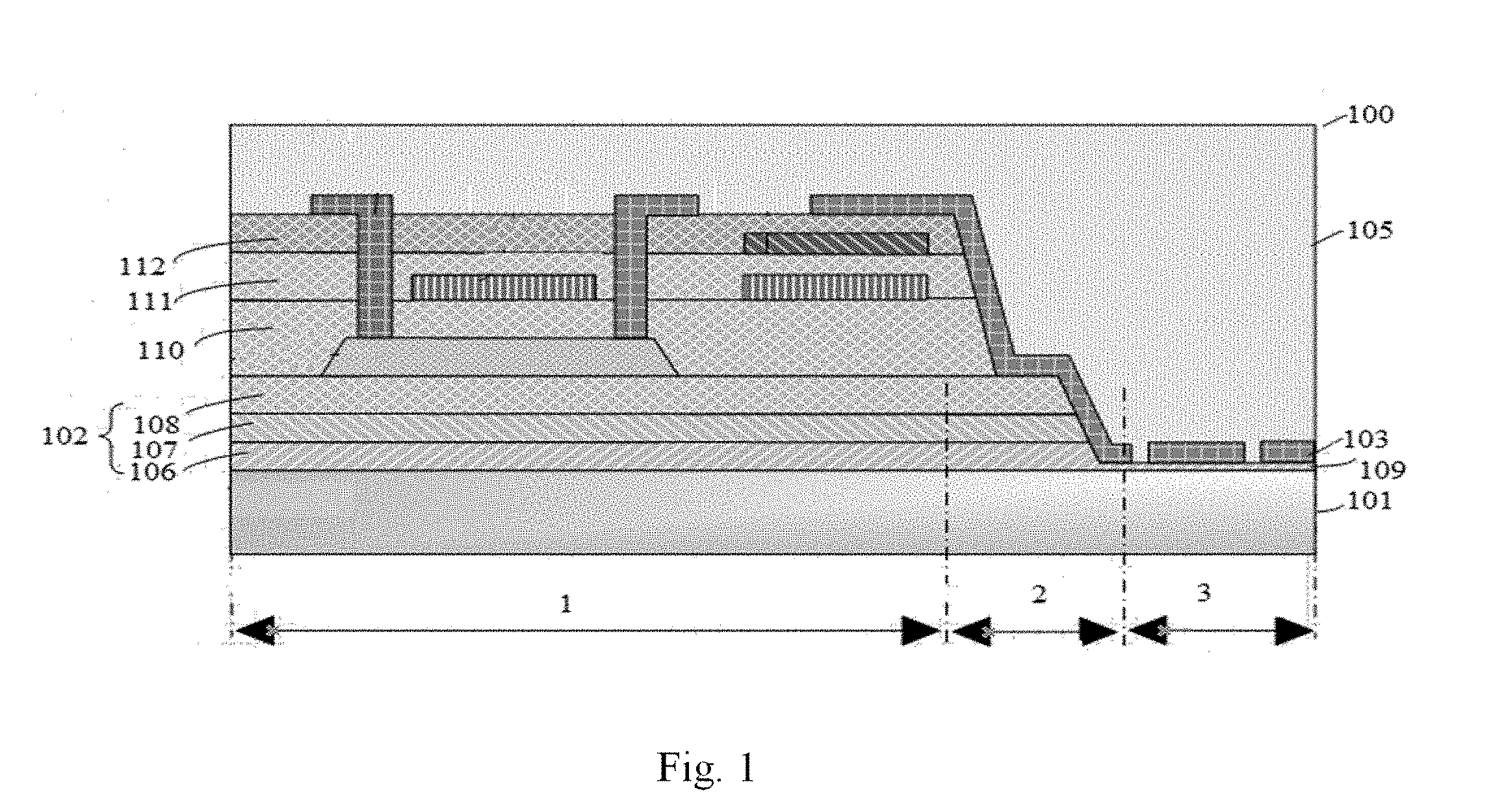
[0026] FIG. 1 is a schematic sectional view of a flexible display panel according to an embodiment of the present application.
[0027] FIG. 2 is a sectional view of a flexible display panel according to another embodiment of the present application.
[0028] FIG. 3 is a schematic flow chart of a manufacturing method of a flexible display panel according to an embodiment of the present application.
[0029] FIG. 4 is a schematic flow chart of a manufacturing method of a flexible display panel according to another embodiment of the present application.
DETAILED DESCRIPTION
[0030] A clear and complete description of technical solutions in the embodiments of the present application will be given below, in combination with the accompanying drawings in the embodiments of the present application. Apparently, the described embodiments are a part of the embodiments of the present application, but not all of the embodiments. All other embodiments, obtained by those skilled in the art based on the embodiments of the present application without creative efforts, shall fall within the protection scope of the present application.
[0031] FIG. 1 is a schematic sectional view of a flexible display panel 100 according to an embodiment of the present application.
[0032] The flexible display panel 100 includes: a flexible substrate 101, a buffer layer 102 formed on the flexible substrate 101, and a metal layer 103 formed on the buffer layer 102. The flexible display panel 100 includes a display area 1 and a bending area 3 in a lateral direction. The buffer layer 102 includes a first portion and a second portion, the first portion corresponds to the display area 1, the second portion corresponds to the bending area 3, and the thickness of the second portion is less than the thickness of the first portion.
[0033] According to embodiments of the present application, the thickness of the buffer layer of the bending area is less than the thickness of the buffer layer of the display area by etching the buffer layer of the bending area before forming the metal layer, and thereby the bending ability of the flexible display panel is improved.
[0034] According to embodiments of the present application, the first portion of the buffer layer 102 may include a first SIOx layer 106, a SINx layer 107 and a second SIOx layer 108 that are successively disposed, and the second portion of the buffer layer 102 includes a first SIOx layer, and does not include a SINx layer or a second SIOx layer.
[0035] Referring to FIG. 1, in the display area of the flexible display panel, the buffer layer may include the first SIOx layer 106, the SINx layer 107, and the second SIOx layer 108 (i.e., the first portion) that are successively disposed from bottom to top. In the bending area of the flexible display panel, the buffer layer may include a first SIOx layer 109 (i.e., the second portion) that is remained by removing the SINx layer and the second SIOx layer. The first SIOx layer 106 and the first SIOx layer 109 are on the same layer.
[0036] It should be understood that the first portion of the buffer layer 102 may include at least one layer of the first SIOx layer, the SINx layer and the second SIOx layer, and embodiments of the present application are not limited to a setting sequence of each layer. Alternatively, the buffer layer 102 may also be other silicon compounds or other materials that may be used for the buffer layer.
[0037] Further, the thickness of the first SIOx layer 109 of the second portion is less than or equal to the thickness of the first SIOx layer 106 of the first portion. For example, the thickness of the first portion may be from 300 nm to 1400 nm. The thickness of the second portion may be from 10 nm to 100 nm.
[0038] Preferably, the thickness of the second portion may be 10 nm to 30 nm.
[0039] Optionally, as another embodiment, a flexible display panel 100 further includes a planarization layer 105.
[0040] For example, the flexible display panel 100 includes a flexible substrate 101, a buffer layer 102, a metal layer 103 and a planarization layer 105 that are successively formed on the flexible substrate 101. The thickness of the buffer layer of the bending area is less than the thickness of the buffer layer of the display area. The planarization layer 105 may be made of an organic material. The buffer layer 102 may be made of, for example, an inorganic insulating material. For example, the inorganic insulating material may be an inorganic silicon material, and specifically may be silicon nitride, silicon oxide or the like. In general, when the inorganic silicon material is used for the buffer layer, for example, metal lines breakage in the metal layer is easily caused when the flexible display panel is bent. In general, the thinner the thickness of the buffer layer of the bending area, the stronger the bending ability of the metal layer of the bending area. When the thickness of the buffer layer of the bending area is very small, the metal layer of the bending area is located between organic layers, and a risk of the metal layer of the bending area being broken is greatly reduced when being bent. The bending ability of a bending area of a flexible screen body may be increased by reducing the thickness of the buffer layer of the bending area.
[0041] Optionally, as another embodiment, a flexible substrate 101 further includes a transition area 2 in a lateral direction. The transition area 2 is located between a display area 1 and a bend area 3. A buffer layer 102 further includes a third portion, which corresponds to the transition area 2, and gradually decreases in width in a direction from the flexible substrate 101 toward a metal layer 103. The thickness of the third portion is from 300 nm to 700 nm. A role of the transition area 2 is to reduce a risk of lines breakage when the metal layer climbs a slope, and the thickness of the third portion is thinned in order to reduce a risk of lines breakage when the metal layer is bent.
[0042] According to embodiments of the present application, the metal layer 103 may be the metal lines.
[0043] FIG. 2 is a sectional view of a flexible display panel 200 according to another embodiment of the present application. The flexible display panel 100 includes a flexible substrate 101; a buffer layer 102 formed on the flexible substrate 101; and a metal layer 103, a passivation layer 104 and the planarization layer 105 formed on the buffer layer 102, and the passivation layer 104 is disposed between the planarization layer 105 and the metal layer 103. The flexible display panel 100 includes a display area 1 and a bending area 3 in a lateral direction. The buffer layer 102 includes a first portion and a second portion, the first portion corresponding to the display area 1, the second portion corresponding to the bending area 3, and the thickness of the second portion is less than the thickness of the first portion.
[0044] According to embodiments of the present application, the thickness of the buffer layer of the bending area is less than the thickness of the buffer layer of the display area by etching the buffer layer of the bending area before forming the metal layer, and thereby the bending ability of the flexible display panel is improved.
[0045] According to embodiments of the present application, the first portion of the buffer layer 102 may include a first SIOx layer 106, a SINx layer 107 and a second SIOx layer 108 that are successively disposed, and the second portion of the buffer layer 102 includes a first SIOx layer, and does not include a SINx layer or a second SIOx layer.
[0046] Referring to FIG. 2, in the display area of the flexible display panel, the buffer layer may include the first SIOx layer 106, the SINx layer 107 and the second SIOx layer 108 (i.e., a first portion) that are successively disposed from bottom to top. In the bending area of the flexible display panel, the buffer layer may include a first SIOx layer 109 (i.e., the second portion) that is remained by removing the SINx layer and the second SIOx layer. The first SIOx layer 106 and the first SIOx layer 109 are on the same layer.
[0047] It should be understood that the first portion of the buffer layer 102 may include at least one layer of the first SIOx layer, the SINx layer and the second SIOx layer, and embodiments of the present application are not limited to a setting sequence of each layer. Alternatively, the buffer layer 102 may also be other silicon compounds or other materials that may be used for the buffer layer.
[0048] Further, the thickness of the first SIOx layer 109 of the second portion is less than or equal to the thickness of the first SIOx layer 106 of the first portion. For example, the thickness of the first portion may be from 300 nm to 1400 nm. The thickness of the second portion may be from 10 nm to 100 nm.
[0049] Preferably, the thickness of the second portion is from 10 nm to 30 nm.
[0050] Optionally, as another embodiment, a flexible substrate 101 further includes a transition area 2 in the lateral direction. The transition area 2 is located between a display areal and a bending area 3. A buffer layer 102 further includes a third portion, which corresponds to the transition area 2, and gradually decreases in width in a direction from the flexible substrate 101 toward a metal layer 103. The thickness of the third portion is from 300 nm to 700 nm. A role of the transition area 2 is to reduce a risk of lines breakage when the metal layer climbs a slope. And the thickness of the third part is thinned in order to reduce a risk of lines breakage when the metal layer is bent.
[0051] According to embodiments of the present application, the metal layer 103 may be metal lines.
[0052] The passivation layer 104 and the planarization layer 105 may be made of organic materials. The buffer layer 102 may be made of, for example, an inorganic insulating material. For example, the inorganic insulating material may be inorganic silicon material, and specifically may be silicon nitride, silicon oxide or the like. In general, when the inorganic silicon material is used for the buffer layer, for example, metal lines breakage in the metal layer is easily caused when the flexible display panel is bent. In general, the thinner the thickness of the buffer layer of the bending area, the stronger the bending ability of the metal layer of the bending area. When the thickness of the buffer layer of the bending area is very small, the metal layer of the bending area is located between organic layers, and a risk of the metal layer of the bending area being broken is greatly reduced when being bent. The bending ability of the bending area of a flexible screen body may be increased by reducing the thickness of the buffer layer of the bending area.
[0053] FIG. 3 is a schematic flow chart of a manufacturing method of a flexible display panel according to an embodiment of the present application. The flexible display panel includes a display area and a bending area in a lateral direction. The manufacturing method of FIG. 3 is configured to prepare the flexible display panel of the embodiments of FIG. 1 and FIG. 2. The manufacturing method of FIG. 3 includes the following contents.
[0054] 301: forming a buffer layer on a flexible substrate.
[0055] 302: etching the portion of the buffer layer corresponding to the bending area to obtain a second portion, the portion of the buffer layer corresponding to a display area is used as a first portion, and the thickness of the second portion is less than the thickness of the first portion.
[0056] 303: forming a metal layer on the buffer layer.
[0057] According to embodiments of the present application, the thickness of the buffer layer of the bending area is less than the thickness of the buffer layer of the display area by etching the buffer layer of the bending area before forming the metal layer, and thereby the bending ability of the flexible display panel is improved.
[0058] According to embodiments of the present application, a first SIOx layer, a SINx layer and a second SIOx layer may be formed on the flexible substrate successively when the buffer layer is formed, and the second SIOx layer and the SINx layer of the buffer layer corresponding to the bending area may be etched to expose a first SIOx layer of the second portion.
[0059] Optionally, as another embodiment, a first SIOx layer of a second portion may be further etched when a buffer layer is formed, till the thickness of the first SIOx layer of the second portion is less than or equal to the thickness of a first SIOx layer of a first portion.
[0060] In an embodiment, a flexible display panel further includes a transition area in a lateral direction, and the transition area is located between a display area and a bending area. The manufacturing method of FIG. 3 further includes: etching the portion of a buffer layer corresponding to the transition area to obtain a third portion which gradually decreases in width in a direction from a flexible substrate toward a metal layer.
[0061] According to embodiments of the present application, the thickness of the second portion is from 10 nm to 30 nm.
[0062] According to embodiments of the present application, the metal layer includes metal lines.
[0063] FIG. 4 is a schematic flow chart of a manufacturing method of a flexible display panel according to another embodiment of the present application. The manufacturing method of FIG. 4 is an example of the manufacturing method of FIG. 3, and is for preparing the flexible display panel of the embodiments of FIG. 1 and FIG. 2. The manufacturing method of FIG. 4 includes the following contents.
[0064] 401: forming a buffer layer on a flexible substrate.
[0065] 402: forming a first SIOx layer, a SINx layer and a second SIOx layer on the entire flexible substrate successively.
[0066] 403: etching the second SIOx layer and the SINx layer of the buffer layer corresponding to a bending area to expose a first SIOx layer of the second portion.
[0067] 404: etching the first SIOx layer of the second portion, till the thickness of the first SIOx layer of the second portion is less than or equal to the thickness of the first SIOx layer of the first portion.
[0068] 405: etching the portion of the buffer layer corresponding to a transition area to obtain a third portion which gradually decreases in width in a direction from the flexible substrate toward the metal layer.
[0069] 406: forming a gate insulating layer 110, a capacitor insulating layer 111 and an interlayer dielectric layer 112 on the buffer layer.
[0070] 407: forming a metal layer on the interlayer dielectric layer 112. That is, the metal layer may cover the interlayer dielectric layer 112 and the second portion and the third portion of the buffer layer.
[0071] 408: forming a passivation layer on the metal layer.
[0072] 409: forming a planarization layer on the passivation layer.
[0073] It should be understood that 408 and 409 are optional. The planarization layer and the passivation layer are made of organic materials. The buffer layer may be made of, for example, an inorganic insulating material. For example, the inorganic insulating material may be inorganic silicon material, and specifically may be silicon nitride, silicon oxide or the like. In general, when the inorganic silicon material is used for the buffer layer, for example, metal lines breakage in the metal layer is easily caused when the flexible display panel is bent. In general, the thinner the thickness of the buffer layer of the bending area, the stronger the bending ability of the metal layer of the bending area. When the thickness of the buffer layer of the bending area is very small, the metal layer of the bending area is located between organic layers, and a risk of the metal layer of the bending area being broken is greatly reduced when being bent. At the same time, a thinner inorganic layer may prevent the organic material from contaminating a chamber when etching and depositing. The bending ability of the bending area of a flexible screen body may be increased by reducing the thickness of the buffer layer of the bending area. In addition, the buffer layer of the bending area is etched before the metal layer is deposited, which is a relatively simple manufacturing process, and accordingly to save cost.
[0074] The above descriptions are merely preferred embodiments of the present application, but not intended to limit the present application. Any modification and equivalent replacement made without departing from the spirit and principle of the present application shall fall within the protection scope of the present application.
* * * * *
D00000
D00001
D00002
D00003
XML
uspto.report is an independent third-party trademark research tool that is not affiliated, endorsed, or sponsored by the United States Patent and Trademark Office (USPTO) or any other governmental organization. The information provided by uspto.report is based on publicly available data at the time of writing and is intended for informational purposes only.
While we strive to provide accurate and up-to-date information, we do not guarantee the accuracy, completeness, reliability, or suitability of the information displayed on this site. The use of this site is at your own risk. Any reliance you place on such information is therefore strictly at your own risk.
All official trademark data, including owner information, should be verified by visiting the official USPTO website at www.uspto.gov. This site is not intended to replace professional legal advice and should not be used as a substitute for consulting with a legal professional who is knowledgeable about trademark law.