Controller, Operating Method Thereof And Memory System
BYUN; Eu-Joon
U.S. patent application number 16/058302 was filed with the patent office on 2019-07-04 for controller, operating method thereof and memory system. The applicant listed for this patent is SK hynix Inc.. Invention is credited to Eu-Joon BYUN.
| Application Number | 20190205256 16/058302 |
| Document ID | / |
| Family ID | 67057819 |
| Filed Date | 2019-07-04 |


View All Diagrams
| United States Patent Application | 20190205256 |
| Kind Code | A1 |
| BYUN; Eu-Joon | July 4, 2019 |
CONTROLLER, OPERATING METHOD THEREOF AND MEMORY SYSTEM
Abstract
A controller includes an address manager suitable for mapping a first information indicating a start map data of a continuous map data, and a second information indicating a number of the continuous map data, and suitable for storing the first and second information; and a processor suitable for controlling, when a read request for a target map data is received, a memory device to read out the target map data from a meta region of the memory device based on the first information and the second information.
| Inventors: | BYUN; Eu-Joon; (Gyeonggi-do, KR) | ||||||||||
| Applicant: |
|
||||||||||
|---|---|---|---|---|---|---|---|---|---|---|---|
| Family ID: | 67057819 | ||||||||||
| Appl. No.: | 16/058302 | ||||||||||
| Filed: | August 8, 2018 |
| Current U.S. Class: | 1/1 |
| Current CPC Class: | G06F 12/1027 20130101; G06F 2212/608 20130101; G06F 2212/602 20130101; G06F 12/0862 20130101; G06F 2212/1024 20130101; G06F 12/0246 20130101; G06F 2212/654 20130101; G06F 12/0292 20130101; G06F 12/10 20130101; G06F 2212/2022 20130101 |
| International Class: | G06F 12/10 20060101 G06F012/10; G06F 12/0862 20060101 G06F012/0862; G06F 12/02 20060101 G06F012/02 |
Foreign Application Data
| Date | Code | Application Number |
|---|---|---|
| Jan 3, 2018 | KR | 10-2018-0000529 |
Claims
1. A controller comprising: an address manager suitable for mapping a first information indicating a start map data of a continuous map data, and a second information indicating a number of the continuous map data, and suitable for storing the first and second information; and a processor suitable for controlling, when a read request for a target map data is received, a memory device to read out the target map data from a meta region of the memory device based on the first information and the second information.
2. The controller of claim 1, wherein the processor controls the memory device to prefetch and read the target map data based on the second information.
3. The controller of claim 1, wherein the processor caches map data stored in the meta region of the memory device and periodically updates the first information and the second information.
4. The controller of claim 3, wherein the processor controls, when a cache miss occurs, the memory device to read out map data corresponding to data stored in a user region of the memory device, and updates the first information and the second information based on the read-out map data.
5. The controller of claim 1, wherein the processor controls the memory device to store the continuous map data along with the first information and the second information into the meta region of the memory device.
6. The controller of claim 1, wherein the processor determines whether the target map data is a continuous map data based on the second information.
7. The controller of claim 1, wherein the map data includes units of segments.
8. An operating method of a controller, the method comprising: mapping a first information indicating a start map data of a continuous map data and a second information indicating a number of the continuous map data, and storing the first and second information; and controlling, when a read request for a target map data is received, a memory device to read out the target map data from a meta region of the memory device based on the first information and the second information.
9. The method of claim 8, further comprising controlling the memory device to prefetch and read the target map data based on the second information.
10. The method of claim 8, further comprising caching map data stored in the meta region of the memory device and periodically updating the first information and the second information.
11. The method of claim 10, further comprising controlling, when a cache miss occurs, the memory device to read out map data corresponding to data stored in a user region of the memory device, and updating the first information and the second information based on the read-out map data.
12. The method of claim 8, further comprising controlling the memory device to store the continuous map data along with the first information and the second information into the meta region of the memory device.
13. The method of claim 8, further comprising determining whether the target map data is a continuous map data based on the second information.
14. The method of claim 8, wherein the map data includes units of segments.
15. A memory system comprising: a memory device including a meta region suitable for storing a map data and a user region suitable for storing a user data; and a controller suitable for controlling the memory device, wherein the controller includes: an address manager suitable for mapping a first information indicating a start map data of a continuous map data, and a second information indicating a number of the continuous map data, and suitable for storing the first and second information; and a processor suitable for controlling, when a read request for a target map data is received, the memory device to read out the target map data from a meta region of the memory device based on the first information and the second information.
16. The memory system of claim 15, wherein the processor controls the memory device to prefetch and read the target map data based on the second information.
17. The memory system of claim 15, wherein the processor caches map data stored in the meta region of the memory device and periodically updates the first information and the second information.
18. The memory system of claim 17, wherein the processor controls, when a cache miss occurs, the memory device to read out map data corresponding to data stored in a user region of the memory device, and updates the first information and the second information based on the read-out map data.
19. The memory system of claim 15, wherein the processor controls the memory device to store the continuous map data along with the first information and the second information into the meta region of the memory device.
20. The memory system of claim 15, wherein the processor determines whether the target map data is a continuous map data based on the second information.
Description
CROSS-REFERENCE TO RELATED APPLICATIONS
[0001] The present application claims priority under 35 U.S.C. .sctn. 119(a) to Korean Patent Application No. 10-2018-0000529 filed on Jan. 3, 2018, the disclosure of which is incorporated herein by reference in its entirety.
BACKGROUND
1. Field
[0002] Various exemplary embodiments of the present invention generally relate to a controller and a memory system. Particularly, the exemplary embodiments relate to a controller capable of efficiently managing data, an operating method thereof, and a memory system including the controller.
2. Description of the Related Art
[0003] The computing environment paradigm is moving towards ubiquitous computing, which enables computing systems to be used anytime and anywhere. As a result, the demand for portable electronic devices, such as mobile phones, digital cameras, and laptop computers are soaring. Those electronic devices generally include a memory system using a memory device as a data storage device. The data storage device may be used as a main memory unit or an auxiliary memory unit of a portable electronic device.
[0004] Since the data storage devices uses a memory device that does not have a mechanical driving unit (e.g., a mechanical arm with a read/write head) as compared with a hard disk device that does have a mechanical driving unit, the data storage device has excellent stability and durability. Also, the data storage device has quicker data access rate and lower power consumption than the hard disk device. Non-limiting examples of the data storage device having such advantages include Universal Serial Bus (USB) memory devices, memory cards of diverse interfaces, Solid-State Drives (SSD) and the like.
SUMMARY
[0005] Various embodiments of the present invention are directed to a controller and a memory system capable of managing a sequence for map data and reading efficiently the map data based on the sequence of the map data.
[0006] In accordance with an embodiment of the present invention, a controller may include: an address manager suitable for mapping a first information indicating a start map data of a continuous map data, and a second information indicating a number of the continuous map data, and suitable for storing the first and second information; and a processor suitable for controlling, when a read request for a target map data is received, a memory device to read out the target map data from a meta region of the memory device based on the first information and the second information.
[0007] In accordance with an embodiment of the present invention, an operating method of controller may include: mapping a first information indicating a start map data of a continuous map data and a second information indicating a number of the continuous map data, and storing the first and second information; and controlling, when a read request for a target map data is received, a memory device to read out the target map data from a meta region of the memory device based on the first information and the second information.
[0008] In accordance with an embodiment of the present invention, a memory system may include a memory device including a meta region suitable for storing a map data and a user region suitable for storing a user data; and a controller suitable for controlling the memory device, wherein the controller includes: an address manager suitable for mapping a first information indicating a start map data of a continuous map data, and a second information indicating a number of the continuous map data, and suitable for storing the first and second information; and a processor suitable for controlling, when a read request for a target map data is received, the memory device to read out the target map data from a meta region of the memory device based on the first information and the second information.
[0009] In accordance with an embodiment of the present invention, a memory system may include a memory device including a meta region suitable for storing a plurality of map data; and a controller suitable for controlling the memory device, wherein the controller includes; an address manager suitable for generating a table including first information and second information, the first information indicating each of the plurality of map data and the second information indicating whether each of the plurality of map data is continuous map data and a number of the continuous map data; and a processor suitable for determining, when a read request is received, a target map data among the plurality of map data based on the first information and the second information and controlling the memory device to read the target map data.
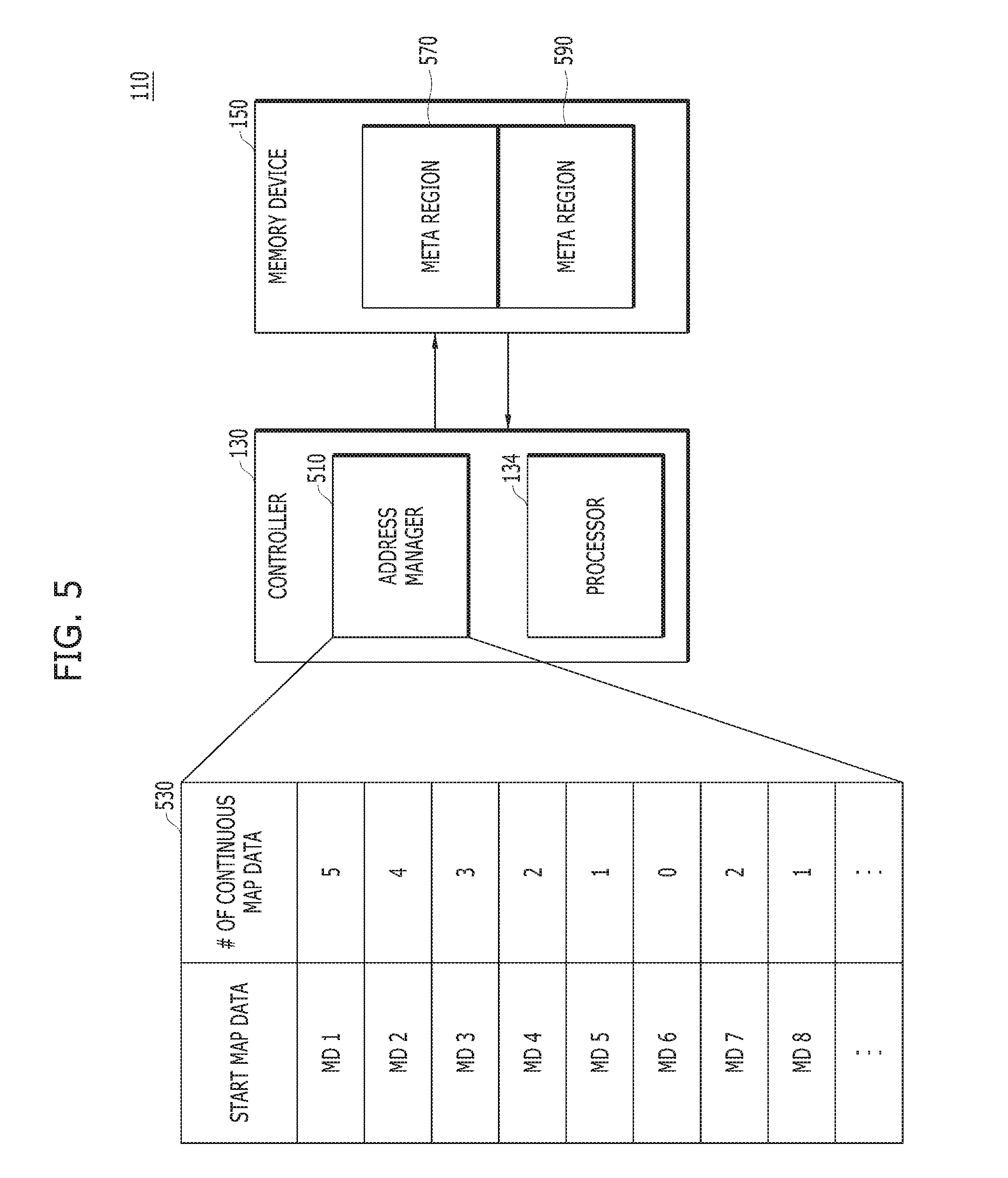
BRIEF DESCRIPTION OF THE DRAWINGS
[0010] The description herein makes reference to the accompanying drawings wherein like reference numerals refer to like parts throughout the several views, and wherein:
[0011] FIG. 1 is a block diagram illustrating a data processing system including a memory system in accordance with an embodiment of the present disclosure;
[0012] FIG. 2 is a schematic diagram illustrating a configuration of a memory device of the memory system shown in FIG. 1;
[0013] FIG. 3 is a circuit diagram illustrating a configuration of a memory cell array of a memory block in the memory device shown in FIG. 2;
[0014] FIG. 4 is a schematic diagram illustrating an exemplary three-dimensional structure of the memory device shown in FIG. 2;
[0015] FIG. 5 is a block diagram illustrating a memory system in accordance with an embodiment of the present disclosure;
[0016] FIG. 6 is a flowchart illustrating an operation of a controller in accordance with an embodiment of the present disclosure;
[0017] FIG. 7 is a flowchart illustrating an operation of a controller in accordance with an embodiment of the present disclosure; and
[0018] FIGS. 8 to 16 are diagrams schematically illustrating application examples of a data processing system, in accordance with various embodiments of the present invention.
DETAILED DESCRIPTION
[0019] Various examples of the disclosure are described below in more detail with reference to the accompanying drawings. The disclosure may be embodied in different other embodiments, forms and variations thereof and should not be construed as being limited to the embodiments set forth herein. Rather, the described embodiments are provided so that this disclosure will be thorough and complete, and will fully convey the disclosure to those skilled in the art to which this invention pertains. Throughout the disclosure, like reference numerals refer to like parts throughout the various figures and examples of the disclosure. It is noted that reference to "an embodiment" does not necessarily mean only one embodiment, and different references to "an embodiment" are not necessarily to the same embodiment(s).
[0020] It will be understood that, although the terms "first", "second", "third", and so on may be used herein to describe various elements, these elements are not limited by these terms. These terms are used to distinguish one element from another element. Thus, a first element described below could also be termed as a second or third element without departing from the spirit and scope of the present invention.
[0021] The drawings are not necessarily to scale and, in some instances, proportions may have been exaggerated in order to clearly illustrate features of the embodiments. When an element is referred to as being connected or coupled to another element, it should be understood that the former can be directly connected or coupled to the latter, or electrically connected or coupled to the latter via an intervening element therebetween.
[0022] It will be further understood that when an element is referred to as being "connected to", or "coupled to" another element, it may be directly on, connected to, or coupled to the other element, or one or more intervening elements may be present. In addition, it will also be understood that when an element is referred to as being "between" two elements, it may be the only element between the two elements, or one or more intervening elements may also be present.
[0023] The terminology used herein is for the purpose of describing particular embodiments only and is not intended to be limiting of the present invention.
[0024] As used herein, singular forms are intended to include the plural forms and vice versa, unless the context clearly indicates otherwise.
[0025] It will be further understood that the terms "comprises," "comprising," "includes," and "including" when used in this specification, specify the presence of the stated elements and do not preclude the presence or addition of one or more other elements. As used herein, the term "and/or" includes any and all combinations of one or more of the associated listed items.
[0026] Unless otherwise defined, all terms including technical and scientific terms used herein have the same meaning as commonly understood by one of ordinary skill in the art to which the present invention belongs in view of the present disclosure. It will be further understood that terms, such as those defined in commonly used dictionaries, should be interpreted as having a meaning that is consistent with their meaning in the context of the present disclosure and the relevant art and will not be interpreted in an idealized or overly formal sense unless expressly so defined herein.
[0027] In the following description, numerous specific details are set forth in order to provide a thorough understanding of the present invention. The present invention may be practiced without some or all of these specific details. In other instances, well-known process structures and/or processes have not been described in detail in order not to unnecessarily obscure the present invention.
[0028] It is also noted, that in some instances, as would be apparent to those skilled in the relevant art, a feature or element described in connection with one embodiment may be used singly or in combination with other features or elements of another embodiment, unless otherwise specifically indicated.
[0029] FIG. 1 is a block diagram illustrating a data processing system 100 in accordance with an embodiment of the present invention.
[0030] Referring to FIG. 1, the data processing system 100 may include a host 102 operatively coupled to a memory system 110.
[0031] Non-limiting examples of the host 102 may include, for example, a portable electronic device such as a mobile phone, an MP3 player and a laptop computer or an electronic device such as a desktop computer, a game player, a television (TV), a projector and the like.
[0032] The memory system 110 may operate or perform a specific function or operation in response to a request from the host 102 and, particularly, may store data to be accessed by the host 102. The memory system 110 may be used as a main memory system or an auxiliary memory system of the host 102. The memory system 110 may be implemented with any one of various types of storage devices, which may be electrically coupled with the host 102, according to a protocol of a host interface. Non-limiting examples of suitable storage devices include a solid state drive (SSD), a multimedia card (MMC), an embedded MMC (eMMC), a reduced size MMC (RS-MMC) and a micro-MMC, a secure digital (SD) card, a mini-SD and a micro-SD, a universal serial bus (USB) storage device, a universal flash storage (UFS) device, a compact flash (CF) card, a smart media (SM) card, a memory stick, and the like.
[0033] The storage devices for the memory system 110 may be implemented with a volatile memory device such as a dynamic random access memory (DRAM) and a static RAM (SRAM) and/or a nonvolatile memory device such as a read only memory (ROM), a mask ROM (MROM), a programmable ROM (PROM), an erasable programmable ROM (EPROM), an electrically erasable programmable ROM (EEPROM), a ferroelectric RAM (FRAM), a phase-change RAM (PRAM), a magneto-resistive RAM (MRAM), a resistive RAM (RRAM or ReRAM) and a flash memory.
[0034] The memory system 110 may include a controller 130 and a memory device 150. The memory device 150 may store data to be accessed by the host 102, and the controller 130 may control storage of data in the memory device 150.
[0035] The controller 130 and the memory device 150 may be integrated into a single semiconductor device, which may be included in the various types of memory systems as exemplified above.
[0036] The memory system 110 may be configured as a part of a computer, an ultra-mobile PC (UMPC), a workstation, a net-book, a personal digital assistant (PDA), a portable computer, a web tablet, a tablet computer, a wireless phone, a mobile phone, a smart phone, an e-book, a portable multimedia player (PMP), a portable game player, a navigation system, a black box, a digital camera, a digital multimedia broadcasting (DMB) player, a 3-dimensional (3D) television, a smart television, a digital audio recorder, a digital audio player, a digital picture recorder, a digital picture player, a digital video recorder, a digital video player, a storage configuring a data center, a device capable of transmitting and receiving information under a wireless environment, one of various electronic devices configuring a home network, one of various electronic devices configuring a computer network, one of various electronic devices configuring a telematics network, a radio frequency identification (RFID) device, or one of various components configuring a computing system.
[0037] The memory device 150 may be a nonvolatile memory device and may retain data stored therein even while an electrical power is not supplied. The memory device 150 may store data provided from the host 102 through a write operation, and provide data stored therein to the host 102 through a read operation. The memory device 150 may include a plurality of memory blocks 152 to 156, each of the memory blocks 152 to 156 may include a plurality of pages. Each of the plurality of pages may include a plurality of memory cells to which a plurality of word lines (WL) are electrically coupled.
[0038] The controller 130 may control overall operations of the memory device 150, such as read, write, program and erase operations. For example, the controller 130 may control the memory device 150 in response to a request from the host 102. The controller 130 may provide the data, read from the memory device 150, with the host 102, and/or may store the data, provided by the host 102, into the memory device 150.
[0039] The controller 130 may include a host interface (I/F) 132, a processor 134, an error correction code (ECC) component 138, a power management unit (PMU) 140, a memory interface (I/F) 142, and a memory 144 all operatively coupled via an internal bus.
[0040] The host interface 132 may process commands and data provided from the host 102, and may communicate with the host 102 through at least one of various interface protocols such as universal serial bus (USB), multimedia card (MMC), peripheral component interconnect-express (PCI-e or PCIe), small computer system interface (SCSI), serial-attached SCSI (SAS), serial advanced technology attachment (SATA), parallel advanced technology attachment (PATA), small computer system interface (SCSI), enhanced small disk interface (ESDI) and integrated drive electronics (IDE).
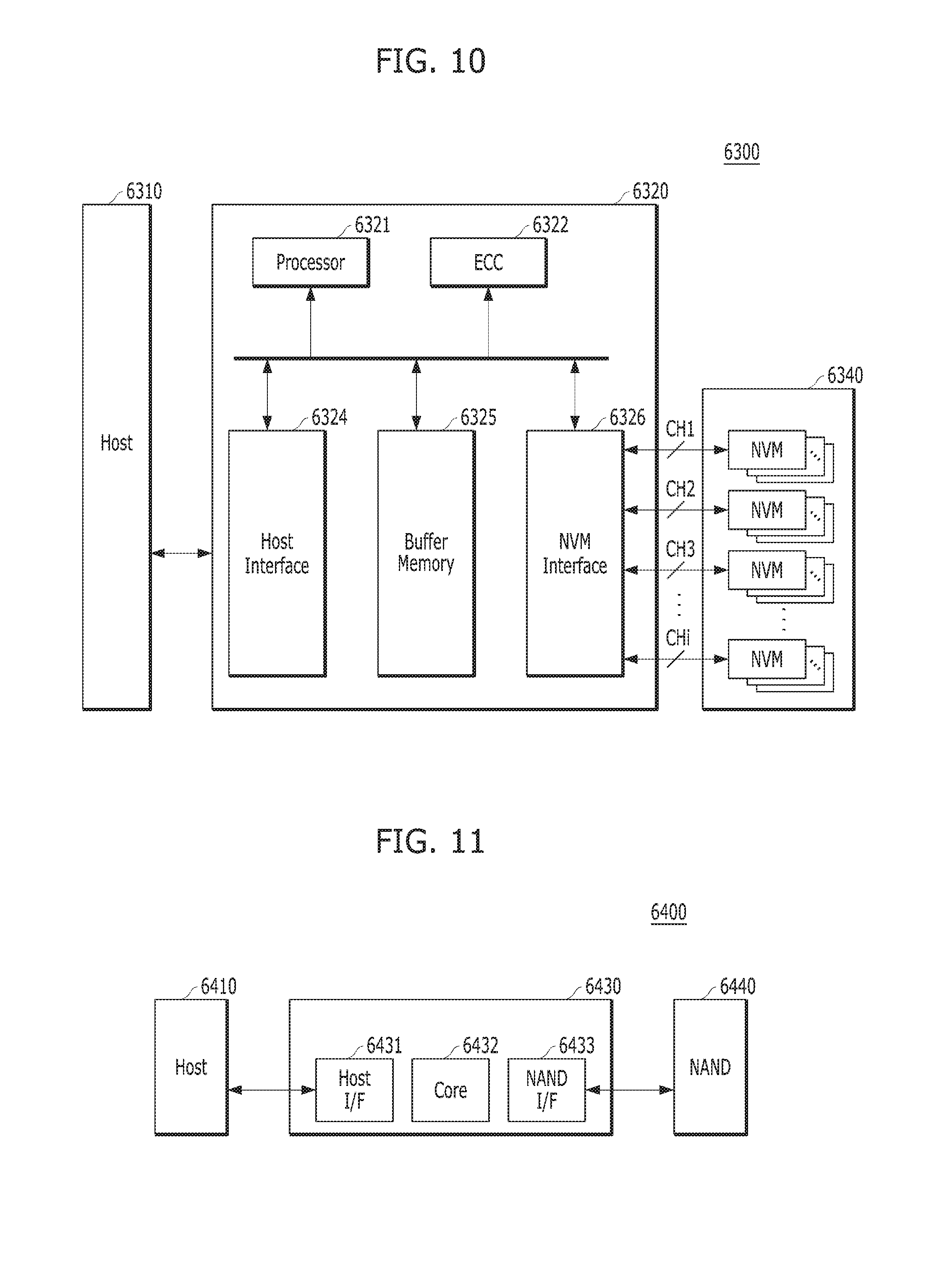
[0041] The ECC component 138 may detect and correct errors in the data read from the memory device 150 during the read operation. When the number of the error bits is greater than or equal to a threshold number of correctable error bits, the ECC component 138 may not correct error bits but may output an error correction fail signal indicating failure in correcting the error bits.
[0042] The ECC component 138 may perform an error correction operation based on a coded modulation such as a low density parity check (LDPC) code, a Bose-Chaudhuri-Hocquenghem (BCH) code, a turbo code, a Reed-Solomon (RS) code, a convolution code, a recursive systematic code (RSC), a trellis-coded modulation (TCM), a Block coded modulation (BCM), and so on. However, the present embodiment is not limited thereto. That is, the ECC component 138 may include all or some of circuits, modules, systems or devices for performing the error correction operation based on at least one of the above described codes.
[0043] The PMU 140 may provide and manage power of the controller 130.
[0044] The memory interface 142 may serve as an interface for handling commands and data transferred between the controller 130 and the memory device 150, to allow the controller 130 to control the memory device 150 in response to a request delivered from the host 102. The memory interface 142 may generate a control signal for the memory device 150 and may process data entered into or outputted from the memory device 150 under the control of the processor 134, in a case when the memory device 150 is a flash memory and, in particular, when the memory device 150 is a NAND flash memory.
[0045] The memory 144 may serve as a working memory of the memory system 110 and the controller 130, and may store temporary or transactional data for operating or driving the memory system 110 and the controller 130. The controller 130 may control the memory device 150 in response to a request from the host 102. The controller 130 may deliver data read from the memory device 150 into the host 102, may store data entered through the host 102 within the memory device 150. The memory 144 may be used to store data required for the controller 130 and the memory device 150 in order to perform these operations.
[0046] The memory 144 may be implemented with a volatile memory. The memory 144 may be implemented with a static random access memory (SRAM) or a dynamic random access memory (DRAM). Although FIG. 1 exemplifies the memory 144 disposed within the controller 130, the disclosure is not limited thereto. That is, the memory 144 may be located inside or outside the controller 130. For instance, the memory 144 may be embodied by an external volatile memory having a memory interface transferring data and/or signals transferred between the memory 144 and the controller 130.
[0047] The processor 134 may control the overall operations of the memory system 110. The processor 134 may drive or execute a firmware to control the overall operations of the memory system 110. The firmware may be referred to as a flash translation layer (FTL).
[0048] A FTL may perform an interfacing operation between the host 102 and the memory device 150. The host 102 may transmit requests for write and read operations to the memory device 150 through the FTL.
[0049] The FTL may manage operations of address mapping, garbage collection, wear-leveling and so forth. Particularly, the FTL may store map data. Therefore, the controller 130 may map a logical address, which is provided from the host 102, to a physical address of the memory device 150 through the map data. The memory device 150 may perform an operation like a general device because of the address mapping operation. Also, through the address mapping operation based on the map data, when the controller 130 updates data of a particular page, the controller 130 may program new data on another empty page and may invalidate old data of the particular page due to a characteristic of a flash memory device. Further, the controller 130 may store map data of the new data into the FTL.
[0050] The processor 134 may be implemented with a microprocessor or a central processing unit (CPU). The memory system 110 may include one or more processors 134.
[0051] A management unit (not shown) may be included in the processor 134. The management unit may perform bad block management of the memory device 150. The management unit may find bad memory blocks included in the memory device 150, which are in unsatisfactory condition for further use, as well as perform bad block management on the bad memory blocks. When the memory device 150 is a flash memory, for example, a NAND flash memory, a program failure may occur during the write operation, for example, during the program operation, due to characteristics of a NAND logic function. During the bad block management, the data of the program-failed memory block or the bad memory block may be programmed into a new memory block. The bad blocks may seriously aggravate the utilization efficiency of the memory device 150 having a 3D stack structure and the reliability of the memory system 100, and thus reliable bad block management is required.
[0052] FIG. 2 is a schematic diagram illustrating the memory device 150.
[0053] Referring to FIG. 2, the memory device 150 may include the plurality of memory blocks BLOCK 0 to BLOCKN-1, and each of the blocks BLOCK 0 to BLOCKN-1 may include a plurality of pages, for example, 2.sup.M pages, the number of which may vary according to circuit design. The memory device 150 may include a plurality of memory blocks, as single level cell (SLC) memory blocks and multi-level cell (MLC) memory blocks, according to the number of bits which may be stored or expressed in each memory cell. The SLC memory block may include a plurality of pages which are implemented with memory cells each capable of storing 1-bit data. The MLC memory block may include a plurality of pages which are implemented with memory cells each capable of storing multi-bit data, for example, two or more-bit data. An MLC memory block including a plurality of pages which are implemented with memory cells that are each capable of storing 3-bit data may be defined as a triple level cell (TLC) memory block.
[0054] FIG. 3 is a circuit diagram illustrating a memory block 330 in the memory device 150.
[0055] Referring to FIG. 3, the memory block 330 may correspond to any of the plurality of memory blocks 152 to 156 included in the memory device 150 of the memory system 110.
[0056] Referring to FIG. 3, the memory block 330 of the memory device 150 may include a plurality of cell strings 340 which are electrically coupled to bit lines BL0 to BLm-1, respectively. The cell string 340 of each column may include at least one drain select transistor DST and at least one source select transistor SST. A plurality of memory cells or a plurality of memory cell transistors MC0 to MCn-1 may be electrically coupled in series between the select transistors DST and SST. The respective memory cells MC0 to MCn-1 may be configured by single level cells (SLC) each of which may store 1 bit of information, or by multi-level cells (MLC) each of which may store data information of a plurality of bits. The strings 340 may be electrically coupled to the corresponding bit lines BL0 to BLm-1, respectively. For reference, in FIG. 3, `DSL` denotes a drain select line, `SSL` denotes a source select line, and `CSL` denotes a common source line.
[0057] While FIG. 3 only shows, as an example, that the memory block 330 includes NAND flash memory cells, it is to be noted that the memory block 330 of the memory device 150 according to the embodiment is not limited to a NAND flash memory. The memory block 330 may be realized by a NOR flash memory, a hybrid flash memory in which at least two kinds of memory cells are combined, or one-NAND flash memory in which a controller is built in a memory chip. The operational characteristics of a semiconductor device may be applied to not only a flash memory device in which a charge storing layer is configured by conductive floating gates but also a charge trap flash (CTF) in which a charge storing layer is configured by a dielectric layer.
[0058] A power supply circuit 310 of the memory device 150 may provide word line voltages, for example, a program voltage, a read voltage and a pass voltage, to be supplied to respective word lines according to an operation mode and voltages to be supplied to bulks, for example, well regions in which the memory cells are formed. The power supply circuit 310 may perform a voltage generating operation under the control of a control circuit (not shown). The power supply circuit 310 may generate a plurality of variable read voltages to generate a plurality of read data, select one of the memory blocks or sectors of a memory cell array under the control of the control circuit, select one of the word lines of the selected memory block, and provide the word line voltages to the selected word line and unselected word lines.
[0059] A read and write (read/write) circuit 320 of the memory device 150 may be controlled by the control circuit, and may serve as a sense amplifier or a write driver according to an operation mode. During a verification operation or a normal read operation, the read/write circuit 320 may operate as a sense amplifier for reading data from the memory cell array. During a program operation, the read/write circuit 320 may operate as a write driver for driving bit lines according to data to be stored in the memory cell array. During a program operation, the read/write circuit 320 may receive from a buffer (not illustrated) data to be stored into the memory cell array, and drive bit lines according to the received data. The read/write circuit 320 may include a plurality of page buffers 322 to 326 respectively corresponding to columns (or bit lines) or column pairs (or bit line pairs), and each of the page buffers 322 to 326 may include a plurality of latches (not illustrated).
[0060] FIG. 4 is a schematic diagram illustrating a three-dimensional (3D) structure of the memory device 150.
[0061] Although FIG. 4 shows a 3D structure, it is to be noted that the memory device 150 may be embodied by a two-dimensional (2D) or 3D memory device. Specifically, as illustrated in FIG. 4, the memory device 150 may be embodied in a nonvolatile memory device having a 3D stack structure. When the memory device 150 has a 3D structure, the memory device 150 may include a plurality of memory blocks BLK0 to BLKN-1 each having a 3D structure (or a vertical structure).
[0062] Referring again to FIG. 1, when the host 102 issues a read request to the controller 130, the controller 130 may detect a logical block address corresponding to the read request and may cache a location of a physical address corresponding to the logical block address from a map data stored in a meta region of the memory device 150. However, when the map data is not stored in the meta region of the memory device 150, that is, when a cache miss occurs, the controller 130 may search for and read a location of the physical address stored in a user region of the memory device 150. However, such operation degrades the performance of the controller 130 for performing the read operation. Further, such cache miss affects adversely the overhead of the controller and thus should be improved.
[0063] In accordance with an embodiment of the present invention, the controller 130 may reduce the overhead caused by the cache miss during the continuous read operation that produces the continuous data. Further, in accordance with an embodiment of the present invention, the controller 130 may perform a read operation for the continuous data effectively. Described with reference to FIGS. 5 to 7 will be an embodiment of the present invention.
[0064] FIG. 5 is a block diagram illustrating a memory system, for example, the memory system 110 of FIG. 1 in accordance with an embodiment of the present invention.
[0065] Referring to FIG. 5, as shown in FIG. 1, the memory system 110 may include the controller 130 and the memory device 150. The controller 130 may include the processor 134 and an address manager 510. The cell array 330 of the memory device 150 may be divided into a meta region 570 for storing a map data and a user region 590 for storing user data. For the convenience, it is assumed that the map data is configured by units of segments.
[0066] The address manager 510 may generate a continuity table 530 representing whether the map data is continuous. The address manager 510 may generate the continuity table 530 such that a number of continuous map data, which is continuous from a start map data START MAP DATA, corresponds to the start map data START MAP DATA. In other words, the address manager 510 may generate a first information indicating a start map data of a continuous map data and a second information indicating a number of the continuous map data, and store the first and second information in the continuity table 530. For example, it is assumed that the continuous map data comprises first to fifth map data MD1 to MD5. The address manager 510 may store the first map data MD1 indicating a start map data of a continuous map data and a value of five (5) indicating a number of the continuous map data, in the continuity table 530, thereby indicating the continuous map data comprises five (5) numbers of map data starting from the first map data MD1. Also, the address manager 510 may store the second map data MD2 and a value of four (4) in the continuity table 530 thereby indicating the continuous map data comprises four (4) numbers of map data starting from the second map data MD2. In the same way, the address manager 510 may store the third map data MD3 and a value of three (3), the fourth map data MD4 and a value of two (2), and the fifth map data MD5 and a value of one (1) in the continuity table 530. Further, FIG. 5 exemplifies the continuity table 530 representing a sixth map data MD6 and the corresponding value of zero (0) to indicate that the sixth map data MD6 is not a continuous map data. FIG. 5 also exemplifies the continuity table 530 representing a seventh map data MD7 and the corresponding value of two (2) to indicate that another continuous map data comprises the seventh map data MD7 and an eighth map data MD8.
[0067] The processor 134 may cache the map data stored in the meta region 570 of the memory device 150. However, as described above, the processor 134 may search data stored in the user region 590 of the memory device 150 to detect a map data when the cache miss occurs. Further, the address manager 510 may periodically update the continuity table 530 based on the detected map data.
[0068] The processor 134 may control the memory device 150 to read a continuous map data from the meta region 570 according to the continuity table 530. Also, the processor 134 may prefetch a continuous map data according to the continuity table 530. The processor 134 may control the memory device 150 to effectively perform a read operation for a target map data based on the continuity of the continuous map data. For example, when a read request for the first to fifth map data MD1 to MD5 is provided, the processor 134 may control the memory device 150 to read out all of the five (5) map data starting from the first map data MD1 (i.e., the first to fifth map data MD1 to MD5) by detecting the first map data MD1. The processor 134 may control the memory device 150 to prepare a read operation for the second map data MD2 while reading out the first map data MD1. In the same manner, the processor 134 may control the memory device 150 to read out the second to fifth map data MD2 to MD5 according to the continuity table 530. Further, when a read request for the third map data MD3 is provided, the processor 134 may control the memory device 150 to read out three (3) map data starting from the third map data MD3 (i.e., the third to fifth map data MD3 to MD5) by detecting the third map data MD3 in the continuity table 530. The processor 134 may control the memory device 150 to prepare a read operation for the fourth map data MD4 while reading out the third map data MD3. In accordance with an embodiment of the present invention, the controller 130 may reduce time required to search for and read out the map data through the predicted read operation or the prefetch operation.
[0069] The processor 134 may update the map data stored in the memory device 150. The processor 134 may read and correct the map data stored in the memory device 150 based on the continuity table 530 managed by the address manager 510.
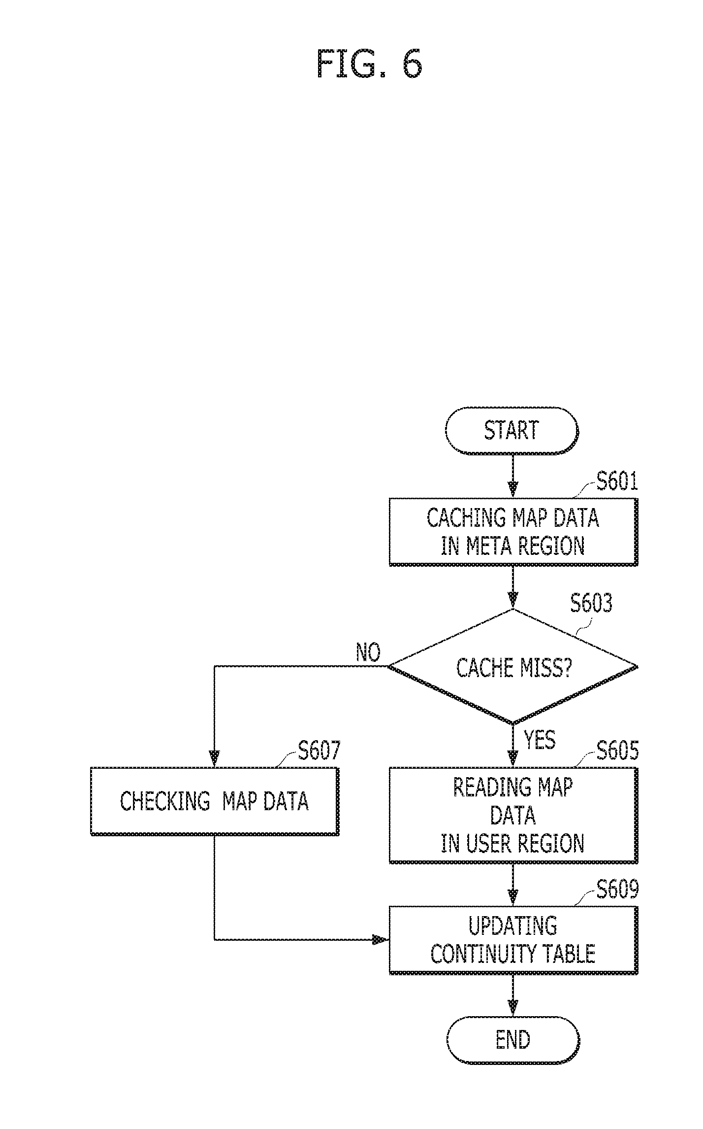
[0070] FIG. 6 is a flowchart illustrating an operation of a controller, for example, the controller 130 of FIG. 5, in accordance with an embodiment of the present invention. In particular, FIG. 6 schematically shows an operation of the address manager 510 for updating the continuity table 530.
[0071] At step S601, the processor 134 may cache a target map data, which is a target of the update, from the meta region 570 of the memory device 150. That is, the processor 134 may detect the target map data.
[0072] At step S603, the processor 134 may determine whether a cache miss for the target map data occurs. The processor 134 may cache the target map data when the target map data is stored in the meta region 570 of the memory device 150. However, the processor 134 may not cache the target map data, which is referred to as a cache miss, when the target map data is not stored in the meta region 570 of the memory device 150.
[0073] When a cache miss occurs ("YES" at step S603), the processor 134 may control the memory device 150 to individually read out the target map data corresponding to the data stored in the user region 590 of the memory device 150 at step S605.
[0074] When the target map data is successfully cached ("NO" at step S603), the processor 134 may check the cached target map data at step S607.
[0075] At step S609, after performing steps S605 or S607, the processor 134 may update the continuity table 530 stored in the address manager 510 based on the target map data.
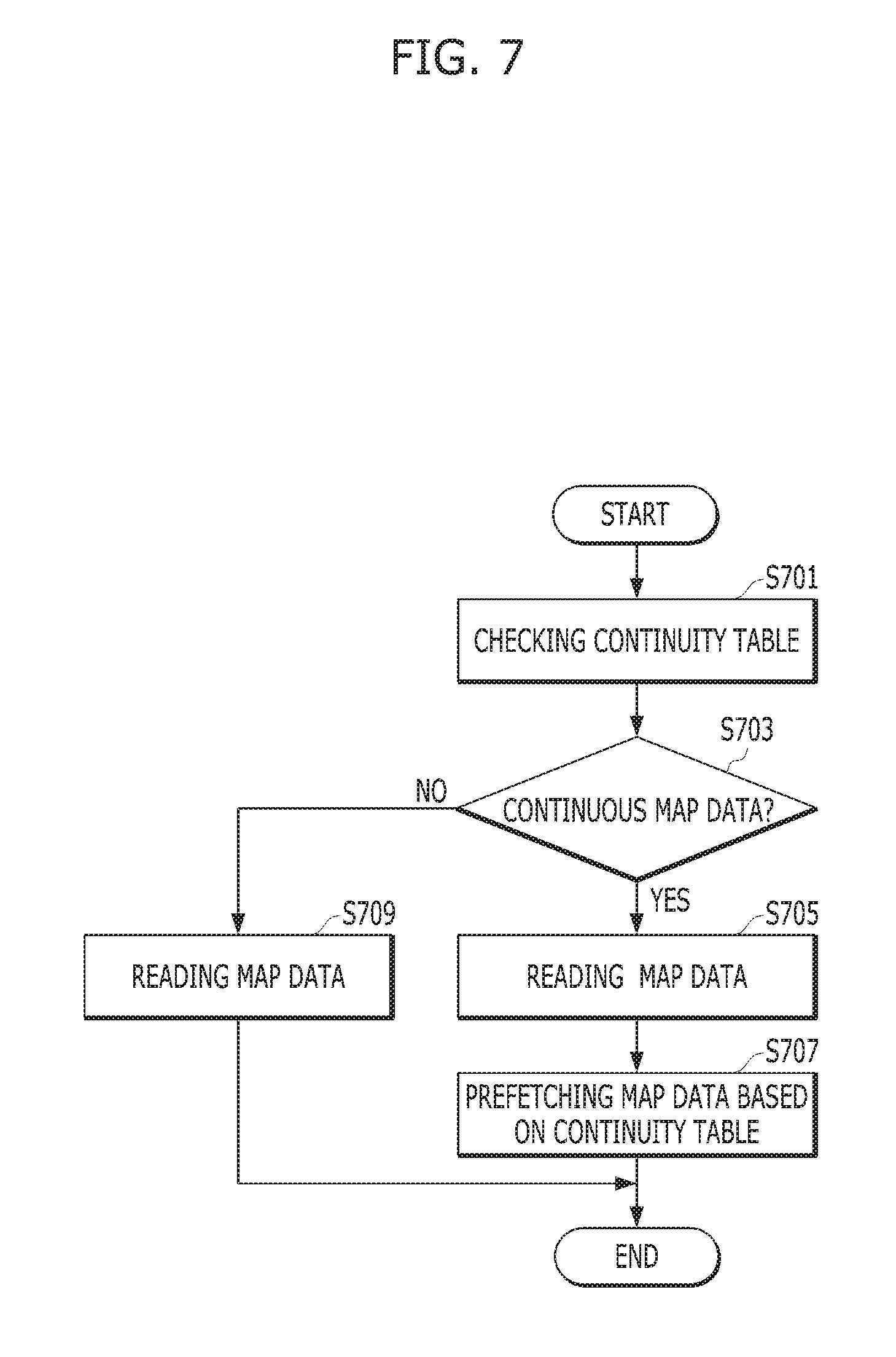
[0076] FIG. 7 is a flowchart illustrating an operation of a controller, for example, the controller 130 of FIG. 5, in accordance with an embodiment of the present invention. Particularly, FIG. 7 illustrates a read operation based on the continuity table 530. For the convenience, it is assumed that the host 102 issues a read request for a target map data.
[0077] At step S701, the processor 134 may check the continuity table 530, in which continuity information for the target map data corresponding to the read request is stored.
[0078] At step S703, the processor 134 may determine whether the target map data is a continuous map data by checking the number of continuous map data corresponding to the target map data in the continuity table 530. When the number of continuous map data corresponding to the target map data has a value of zero (0), the target map data may be determined as not the continuous map data. When the number of continuous map data corresponding to the target map data has a non-zero value, the target map data may be determined as the continuous map data.
[0079] When the target map data is determined as the continuous data ("YES" at step S703), the processor 134 may control the memory device 150 to read out the target map data at step S705.
[0080] At step S707, the processor 134 may prefetch the continuous map data including the target map data according to the continuity of the target map based on the continuity table 530.
[0081] When the target map data is determined as not the continuous data ("NO" at step S703), the processor 134 may control the memory device 150 to read out only the target map data at step S709.
[0082] In accordance with an embodiment of the present invention, the controller 130 may effectively read the continuous map data according to information of the number of the continuous map data. Therefore, the overhead that can occur during a read operation may be reduced.
[0083] Hereinafter, a data processing system and electronic devices which may be constituted with the memory system 110 including the memory device 150 and the controller 130, which are described above by referring to FIGS. 1 to 7, will be described in detail with reference to FIGS. 8 to 16.
[0084] FIGS. 8 to 16 are diagrams schematically illustrating application examples of the data processing system of FIGS. 1 to 7 according to various embodiments.
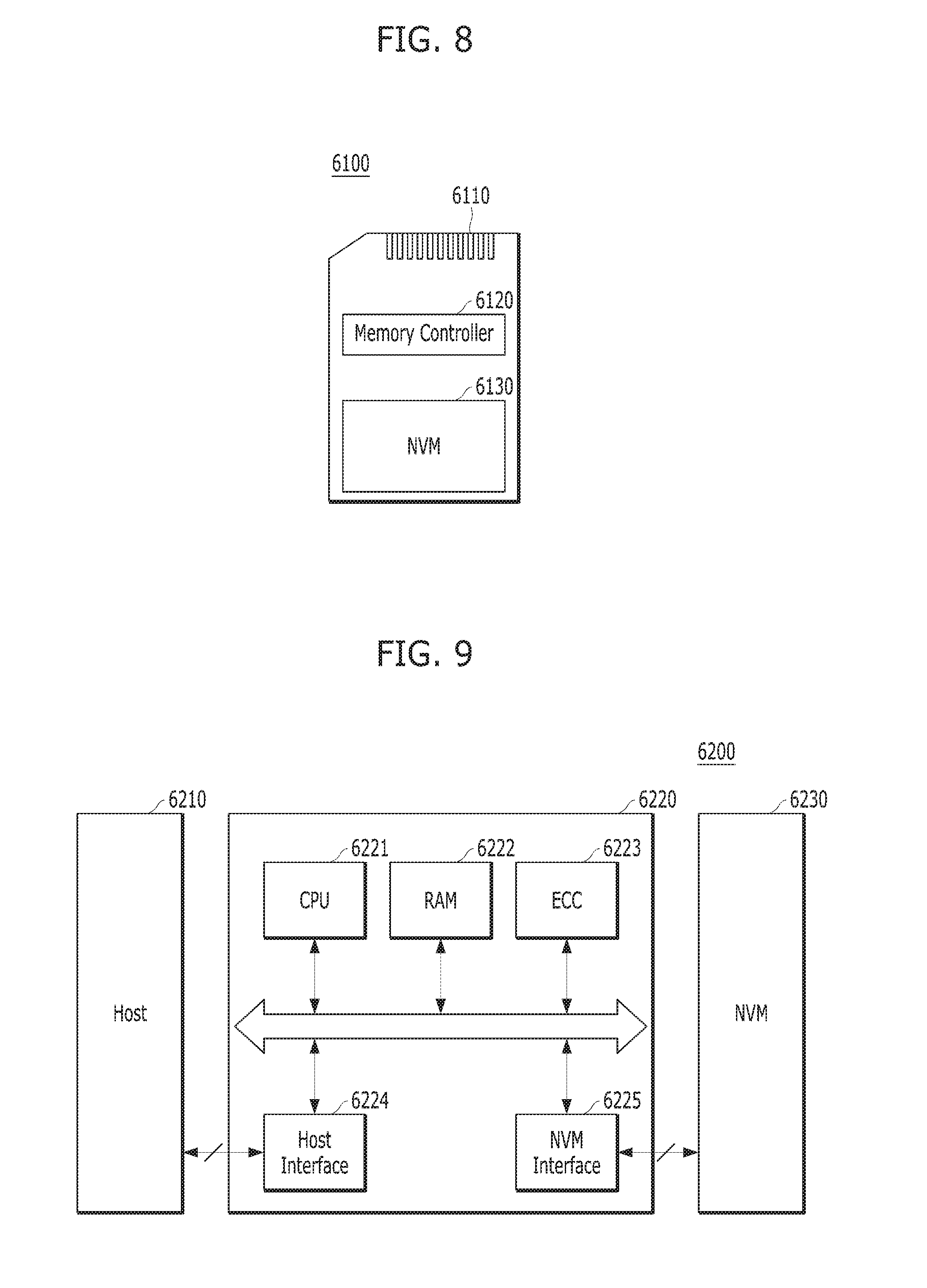
[0085] FIG. 8 is a diagram schematically illustrating an example of the data processing system including the memory system in accordance with an embodiment. FIG. 8 schematically illustrates a memory card system 6100 including the memory system in accordance with an embodiment.
[0086] Referring to FIG. 8, the memory card system 6100 may include a memory controller 6120, a memory device 6130 and a connector 6110.
[0087] More specifically, the memory controller 6120 may be connected to the memory device 6130, and may be configured to access the memory device 6130. The memory device 6130 may be embodied by a nonvolatile memory (NVM). By the way of example but not limitation, the memory controller 6120 may be configured to control read, write, erase and background operations onto the memory device 6130. The memory controller 6120 may be configured to provide an interface between the memory device 6130 and a host (not shown) and/or a drive firmware for controlling the memory device 6130. That is, the memory controller 6120 may correspond to the controller 130 in the memory system 110 described with reference to FIGS. 1 to 7, while the memory device 6130 may correspond to the memory device 150 described with reference to FIGS. 1 to 7.
[0088] Thus, as shown in FIG. 1, the memory controller 6120 may include a random access memory (RAM), a processor, a host interface, a memory interface and an error correction component. The memory controller 130 may further include the elements described in FIG. 1.
[0089] The memory controller 6120 may communicate with an external device, for example, the host 102 of FIG. 1 through the connector 6110. For example, as described with reference to FIG. 1, the memory controller 6120 may be configured to communicate with an external device through one or more of various communication protocols such as universal serial bus (USB), multimedia card (MMC), embedded MMC (eMMC), peripheral component interconnection (PCI), PCI express (PCIe), Advanced Technology Attachment (ATA), Serial-ATA, Parallel-ATA, small computer system interface (SCSI), enhanced small disk interface (EDSI), Integrated Drive Electronics (IDE), Firewire, universal flash storage (UFS), wireless fidelity (WI-Fi or WiFI) and Bluetooth. Thus, the memory system and the data processing system in accordance with an embodiment may be applied to wired and/or wireless electronic devices or particularly mobile electronic devices.
[0090] The memory device 6130 may be implemented by a nonvolatile memory. For example, the memory device 6130 may be implemented by various nonvolatile memory devices such as an erasable and programmable ROM (EPROM), an electrically erasable and programmable ROM (EEPROM), a NAND flash memory, a NOR flash memory, a phase-change RAM (PRAM), a resistive RAM (ReRAM), a ferroelectric RAM (FRAM) and a spin torque transfer magnetic RAM (STT-RAM). The memory device 6130 may include a plurality of dies as in the memory device 150 of FIG. 1.
[0091] The memory controller 6120 and the memory device 6130 may be integrated into a single semiconductor device. For example, the memory controller 6120 and the memory device 6130 may construct a solid state driver (SSD) by being integrated into a single semiconductor device. Also, the memory controller 6120 and the memory device 6130 may construct a memory card such as a PC card (e.g., Personal Computer Memory Card International Association (PCMCIA)), a compact flash (CF) card, a smart media card (e.g., SM and SMC), a memory stick, a multimedia card (e.g., MMC, RS-MMC, MMCmicro and eMMC), a secured digital (SD) card (e.g., SD, miniSD, microSD and SDHC) and a universal flash storage (UFS).
[0092] FIG. 9 is a diagram schematically illustrating another example of a data processing system 6200 including a memory system, in accordance with an embodiment.
[0093] Referring to FIG. 9, the data processing system 6200 may include a memory device 6230 having one or more nonvolatile memories (NVMs) and a memory controller 6220 for controlling the memory device 6230. The data processing system 6200 may serve as a storage medium such as a memory card (e.g., CF, SD, micro-SD or the like) or USB device, as described with reference to FIG. 1. The memory device 6230 may correspond to the memory device 150 in the memory system 110 described in FIGS. 1 to 7, and the memory controller 6220 may correspond to the controller 130 in the memory system 110 described in FIGS. 1 to 7.
[0094] The memory controller 6220 may control a read, write, or erase operation on the memory device 6230 in response to a request of the host 6210, and the memory controller 6220 may include one or more central processing units (CPUs) 6221, a buffer memory such as a random access memory (RAM) 6222, an error correction code (ECC) circuit 6223, a host interface 6224 and a memory interface such as an NVM interface 6225.
[0095] The CPU 6221 may control the operations on the memory device 6230, for example, read, write, file system management and bad page management operations. The RAM 6222 may be operated according to control of the CPU 6221, and used as a work memory, buffer memory or cache memory. When the RAM 6222 is used as a work memory, data processed by the CPU 6221 may be temporarily stored in the RAM 6222. When the RAM 6222 is used as a buffer memory, the RAM 6222 may be used for buffering data transmitted to the memory device 6230 from the host 6210 or transmitted to the host 6210 from the memory device 6230. When the RAM 6222 is used as a cache memory, the RAM 6222 may assist the memory device 6230 to operate at high speed.
[0096] The ECC circuit 6223 may correspond to the ECC component 138 of the controller 130 illustrated in FIG. 1. As described with reference to FIG. 1, the ECC circuit 6223 may generate an error correction code (ECC) for correcting a fail bit or error bit of data provided from the memory device 6230. The ECC circuit 6223 may perform error correction encoding on data provided to the memory device 6230, thereby forming data with a parity bit. The parity bit may be stored in the memory device 6230. The ECC circuit 6223 may perform error correction decoding on data outputted from the memory device 6230. in this case, the ECC circuit 6223 may correct an error using the parity bit. For example, as described with reference to FIG. 1, the ECC circuit 6223 may correct an error using Low Density Parity Check (LDPC) code, Bose-Chaudhri-Hocquenghem (BCH) code, turbo code, Reed-Solomon code, convolution code, Recursive Systematic Code (RSC) or coded modulation such as Trellis-Coded Modulation (TCM) or Block coded modulation (BCM).
[0097] The memory controller 6220 may transmit to, and/or receive from, the host 6210 data or signals through the host interface 6224, and may transmit to, and/or receive from, the memory device 6230 data or signals through the NVM interface 6225. The host interface 6224 may be connected to the host 6210 through a parallel advanced technology attachment (PATA) bus, a serial advanced technology attachment (SATA) bus, a small computer system interface (SCSI), an universal serial bus (USB), a peripheral component interconnect-express (PCIe), or a NAND interface. The memory controller 6220 may have a wireless communication function with a mobile communication protocol such as wireless fidelity (WiFi) or Long Term Evolution (LTE). The memory controller 6220 may be connected to an external device, e.g., the host 6210, or another external device, and then transmit and/or receive data to and/or from the external device. As the memory controller 6220 is configured to communicate with the external device through one or more of various communication protocols, the memory system and the data processing system in accordance with an embodiment may be applied to wired and/or wireless electronic devices or particularly a mobile electronic device.
[0098] FIG. 10 is a diagram schematically illustrating another example of the data processing system including the memory system in accordance with an embodiment. FIG. 10 schematically illustrates a solid state drive (SSD) 6300 to which the memory system in accordance with an embodiment is applied.
[0099] Referring to FIG. 10, the SSD 6300 may include a controller 6320 and a memory device 6340 including a plurality of nonvolatile memories (NVMs). The controller 6320 may correspond to the controller 130 in the memory system 110 of FIG. 1, and the memory device 6340 may correspond to the memory device 150 in the memory system of FIG. 1.
[0100] More specifically, the controller 6320 may be connected to the memory device 6340 through a plurality of channels CH1 to CHi. The controller 6320 may include one or more processors 6321, an error correction code (ECC) circuit 6322, a host interface 6324, a buffer memory 6325 and a memory interface, for example, a nonvolatile memory interface 6326.
[0101] The buffer memory 6325 may temporarily store data provided from the host 6310 or data provided from a plurality of flash memories NVM included in the memory device 6340, or temporarily store meta data of the plurality of flash memories NVM, for example, map data including a mapping table. The buffer memory 6325 may be embodied by volatile memories such as dynamic random access memory (DRAM), a synchronous DRAM (SDRAM), a double data rate (DDR) SDRAM, a low power DDR (LPDDR) SDRAM and a graphics RAM (GRAM) or nonvolatile memories such as a ferroelectric RAM (FRAM), a resistive RAM (RRAM or ReRAM), a spin-transfer torque magnetic RAM (STT-MRAM) and a phase-change RAM (PRAM). For the purpose of description, FIG. 10 illustrates that the buffer memory 6325 exists in the controller 6320, but the buffer memory 6325 may be located or arranged outside the controller 6320.
[0102] The ECC circuit 6322 may calculate an error correction code (ECC) value of data to be programmed to the memory device 6340 during a program operation, perform an error correction operation on data read from the memory device 6340 based on the ECC value during a read operation, and perform an error correction operation on data recovered from the memory device 6340 during a failed data recovery operation.
[0103] The host interface 6324 may provide an interface function with an external device, for example, the host 6310, and the nonvolatile memory interface 6326 may provide an interface function with the memory device 6340 connected through the plurality of channels.
[0104] Furthermore, a plurality of SSDs 6300 to which the memory system 110 of FIG. 1 is applied may be provided to embody a data processing system, for example, a redundant array of independent disks (RAID) system. The RAID system may include the plurality of SSDs 6300 and a RAID controller for controlling the plurality of SSDs 6300. When the RAID controller performs a program operation in response to a write command provided from the host 6310, the RAID controller may select one or more memory systems or SSDs 6300 according to a plurality of RAID levels, i.e., RAID level information of the write command provided from the host 6310 in the SSDs 6300, and may output data corresponding to the write command to the selected SSDs 6300. Furthermore, when the RAID controller performs a read command in response to a read command provided from the host 6310, the RAID controller may select one or more memory systems or SSDs 6300 according to a plurality of RAID levels, that is, RAID level information of the read command provided from the host 6310 in the SSDs 6300, and provide data read from the selected SSDs 6300 to the host 6310.
[0105] FIG. 11 is a diagram schematically illustrating another example of the data processing system including the memory system in accordance with an embodiment. FIG. 11 schematically illustrates an embedded Multi-Media Card (eMMC) 6400 to which the memory system in accordance with an embodiment is applied.
[0106] Referring to FIG. 11, the eMMC 6400 may include a controller 6430 and a memory device 6440 embodied by one or more NAND flash memories. The controller 6430 may correspond to the controller 130 in the memory system 110 of FIG. 1, and the memory device 6440 may correspond to the memory device 150 in the memory system 110 of FIG. 1.
[0107] More specifically, the controller 6430 may be connected to the memory device 6440 through a plurality of channels. The controller 6430 may include one or more cores 6432, a host interface (I/F) 6431 and a memory interface, for example, a NAND interface (I/F) 6433.
[0108] The core 6432 may control the operations of the eMMC 6400. The host interface 6431 may provide an interface function between the controller 6430 and the host 6410. The NAND interface 6433 may provide an interface function between the memory device 6440 and the controller 6430. For example, the host interface 6431 may serve as a parallel interface, for example, MMC interface as described with reference to FIG. 1. Furthermore, the host interface 6431 may serve as a serial interface, for example, Ultra High Speed (UHS)-I and UHS-II interface.
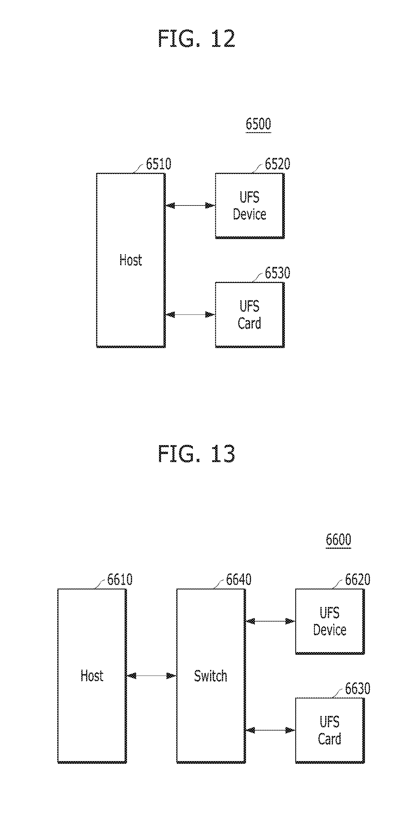
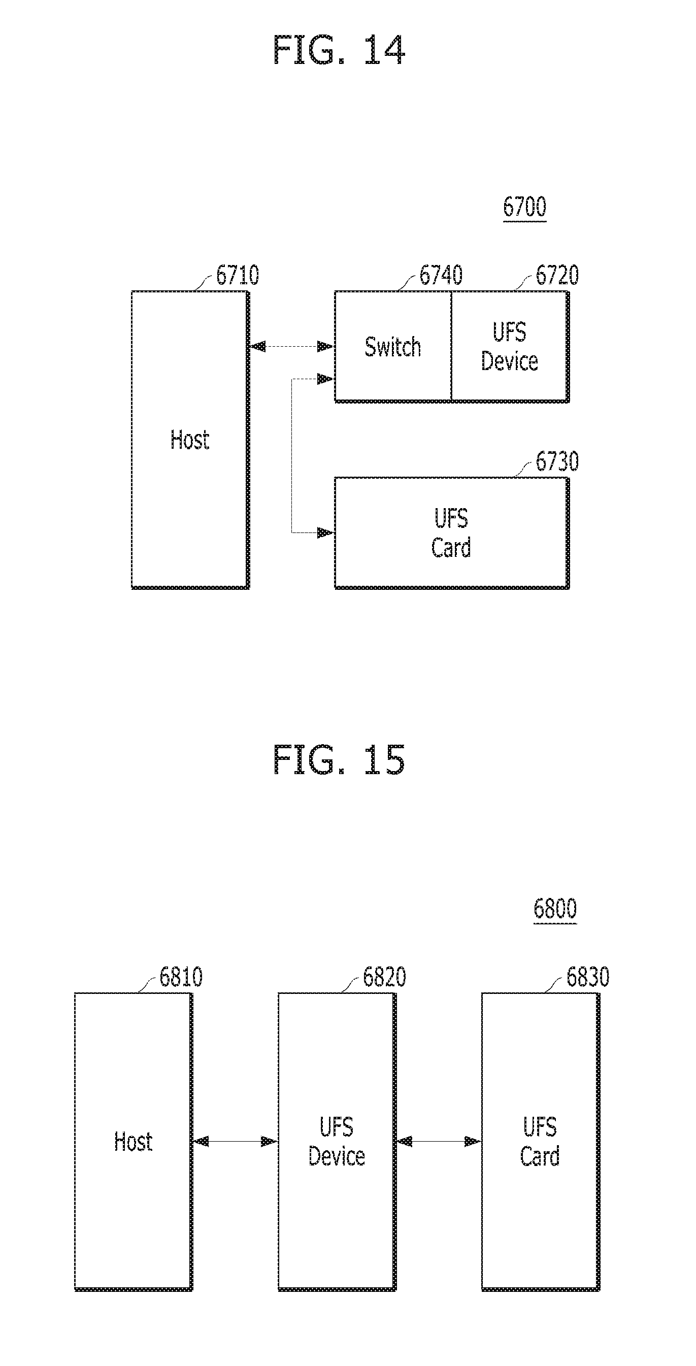
[0109] FIGS. 12 to 15 are diagrams schematically illustrating other examples of the data processing system including the memory system in accordance with an embodiment. FIGS. 12 to 15 schematically illustrate universal flash storage (UFS) systems to which the memory system in accordance with an embodiment is applied.
[0110] Referring to FIGS. 12 to 15, the UFS systems 6500, 6600, 6700 and 6800 may include hosts 6510, 6610, 6710, 6810, UFS devices 6520, 6620, 6720, 6820 and UFS cards 6530, 6630, 6730, 6830, respectively. The hosts 6510, 6610, 6710, 6810 may serve as application processors of wired and/or wireless electronic devices or particularly mobile electronic devices, the UFS devices 6520, 6620, 6720, 6820 may serve as embedded UFS devices. The UFS cards 6530, 6630, 6730, 6830 may serve as external embedded UFS devices or removable UFS cards.
[0111] The hosts 6510, 6610, 6710, 6810, the UFS devices 6520, 6620, 6720, 6820 and the UFS cards 6530, 6630, 6730, 6830 in the respective UFS systems 6500, 6600, 6700 and 6800 may communicate with external devices, e.g., wired and/or wireless electronic devices or particularly mobile electronic devices through UFS protocols. The UFS devices 6520, 6620, 6720, 6820 and the UFS cards 6530, 6630, 6730, 6830 may be embodied by the memory system 110 illustrated in FIG. 1. For example, in the UFS systems 6500, 6600, 6700, 6800, the UFS devices 6520, 6620, 6720, 6820 may be embodied in the form of the data processing system 6200, the SSD 6300 or the eMMC 6400 described with reference to FIGS. 9 to 11, and the UFS cards 6530, 6630, 6730, 6830 may be embodied in the form of the memory card system 6100 described with reference to FIG. 8.
[0112] Furthermore, in the UFS systems 6500, 6600, 6700 and 6800, the hosts 6510, 6610, 6710, 6810, the UFS devices 6520, 6620, 6720, 6820 and the UFS cards 6530, 6630, 6730, 6830 may communicate with each other through an UFS interface, for example, MIPI M-PHY and MIPI UniPro (Unified Protocol) in MIPI (Mobile Industry Processor Interface). Furthermore, the UFS devices 6520, 6620, 6720, 6820 and the UFS cards 6530, 6630, 6730, 6830 may communicate with each other through various protocols other than the UFS protocol, e.g., universal storage bus (USB) Flash Drives (UFDs), multi-media card (MMC), secure digital (SD), mini-SD, and micro-SD.
[0113] In the UFS system 6500 illustrated in FIG. 12, each of the host 6510, the UFS device 6520 and the UFS card 6530 may include UniPro. The host 6510 may perform a switching operation to communicate with at least one of the UFS device 6520 and the UFS card 6530. The host 6510 may communicate with the UFS device 6520 or the UFS card 6530 through link layer switching, e.g., L3 switching at the UniPro. In this case, the UFS device 6520 and the UFS card 6530 may communicate with each other through a link layer switching at the UniPro of the host 6510. In an example, the configuration in which one UFS device 6520 and one UFS card 6530 are connected to the host 6510 has been exemplified for convenience of description. However, a plurality of UFS devices and UFS cards may be connected in parallel or in the form of a star to the host 6510, and a plurality of UFS cards may be connected in parallel or in the form of a star to the UFS device 6520 or connected in series or in the form of a chain to the UFS device 6520. Herein, the form of a star means an arrangement that a single device is coupled with plural other devices or cards for centralized control.
[0114] In the UFS system 6600 illustrated in FIG. 13, each of the host 6610, the UFS device 6620 and the UFS card 6630 may include UniPro, and the host 6610 may communicate with the UFS device 6620 or the UFS card 6630 through a switching module 6640 performing a switching operation, for example, through the switching module 6640 which performs link layer switching at the UniPro, for example, L3 switching. The UFS device 6620 and the UFS card 6630 may communicate with each other through link layer switching of the switching module 6640 at UniPro. In an example, the configuration in which one UFS device 6620 and one UFS card 6630 are connected to the switching module 6640 has been exemplified for convenience of description. However, a plurality of UFS devices and UFS cards may be connected in parallel or in the form of a star to the switching module 6640, and a plurality of UFS cards may be connected in series or in the form of a chain to the UFS device 6620.
[0115] In the UFS system 6700 illustrated in FIG. 14, each of the host 6710, the UFS device 6720 and the UFS card 6730 may include UniPro. The host 6710 may communicate with the UFS device 6720 or the UFS card 6730 through a switching module 6740 performing a switching operation, for example, the switching module 6740 which performs link layer switching at the UniPro, for example, L3 switching. In this case, the UFS device 6720 and the UFS card 6730 may communicate with each other through link layer switching of the switching module 6740 at the UniPro, and the switching module 6740 may be integrated as one module with the UFS device 6720 inside or outside the UFS device 6720. In an example, the configuration in which one UFS device 6720 and one UFS card 6730 are connected to the switching module 6740 has been exemplified for convenience of description. However, a plurality of modules each including the switching module 6740 and the UFS device 6720 may be connected in parallel or in the form of a star to the host 6710 or connected in series or in the form of a chain to each other. Furthermore, a plurality of UFS cards may be connected in parallel or in the form of a star to the UFS device 6720.
[0116] In the UFS system 6800 illustrated in FIG. 15, each of the host 6810, the UFS device 6820 and the UFS card 6830 may include M-PHY and UniPro. The UFS device 6820 may perform a switching operation to communicate with the host 6810 and the UFS card 6830. The UFS device 6820 may communicate with the host 6810 or the UFS card 6830 through a switching operation between the M-PHY and UniPro module for communication with the host 6810 and the M-PHY and UniPro module for communication with the UFS card 6830, for example, through a target Identifier (ID) switching operation. Here, the host 6810 and the UFS card 6830 may communicate with each other through target ID switching between the M-PHY and UniPro modules of the UFS device 6820. In an embodiment, the configuration in which one UFS device 6820 is connected to the host 6810 and one UFS card 6830 is connected to the UFS device 6820 has been exemplified for convenience of description. However, a plurality of UFS devices may be connected in parallel or in the form of a star to the host 6810, or connected in series or in the form of a chain to the host 6810, and a plurality of UFS cards may be connected in parallel or in the form of a star to the UFS device 6820, or connected in series or in the form of a chain to the UFS device 6820.
[0117] FIG. 16 is a diagram schematically illustrating another example of the data processing system including the memory system in accordance with an embodiment. FIG. 16 is a diagram schematically illustrating a user system 6900 to which the memory system in accordance with an embodiment is applied.
[0118] Referring to FIG. 16, the user system 6900 may include a user interface 6910, a memory module 6920, an application processor 6930, a network module 6940, and a storage module 6950.
[0119] More specifically, the application processor 6930 may drive components included in the user system 6900, for example, an operating system (OS), and include controllers, interfaces and a graphic engine which control the components included in the user system 6900. The application processor 6930 may be provided as a System-on-Chip (SoC).
[0120] The memory module 6920 may be used as a main memory, work memory, buffer memory or cache memory of the user system 6900. The memory module 6920 may include a volatile random access memory (RAM) such as a dynamic RAM (DRAM), a synchronous DRAM (SDRAM), a double data rate (DDR) SDRAM, DDR2 SDRAM, DDR3 SDRAM, LPDDR SDARM, LPDDR3 SDRAM or LPDDR3 SDRAM or a nonvolatile RAM such as a phase-change RAM (PRAM), a resistive RAM (ReRAM), a magneto-resistive RAM (MRAM) or a ferroelectric RAM (FRAM). For example, the application processor 6930 and the memory module 6920 may be packaged and mounted, based on Package on Package (PoP).
[0121] The network module 6940 may communicate with external devices. For example, the network module 6940 may not only support wired communication, but may also support various wireless communication protocols such as code division multiple access (CDMA), global system for mobile communication (GSM), wideband CDMA (WCDMA), CDMA-2000, time division multiple access (TDMA), long term evolution (LTE), worldwide interoperability for microwave access (Wimax), wireless local area network (WLAN), ultra-wideband (UWB), Bluetooth, wireless display (WI-DI), thereby communicating with wired/wireless electronic devices or particularly mobile electronic devices. Therefore, the memory system and the data processing system, in accordance with an embodiment of the present invention, can be applied to wired/wireless electronic devices. The network module 6940 may be included in the application processor 6930.
[0122] The storage module 6950 may store data, for example, data received from the application processor 6930, and then may transmit the stored data to the application processor 6930. The storage module 6950 may be embodied by a nonvolatile semiconductor memory device such as a phase-change RAM (PRAM), a magnetic RAM (MRAM), a resistive RAM (ReRAM), a NAND flash, NOR flash and 3D NAND flash, and provided as a removable storage medium such as a memory card or external drive of the user system 6900. The storage module 6950 may correspond to the memory system 110 described with reference to FIG. 1. Furthermore, the storage module 6950 may be embodied as an SSD, eMMC and UFS as described above with reference to FIGS. 10 to 15.
[0123] The user interface 6910 may include interfaces for inputting data or commands to the application processor 6930 or outputting data to an external device. For example, the user interface 6910 may include user input interfaces such as a keyboard, a keypad, a button, a touch panel, a touch screen, a touch pad, a touch ball, a camera, a microphone, a gyroscope sensor, a vibration sensor and a piezoelectric element, and user output interfaces such as a liquid crystal display (LCD), an organic light emitting diode (OLED) display device, an active matrix OLED (AMOLED) display device, an LED, a speaker and a motor.
[0124] Furthermore, when the memory system 110 of FIG. 1 is applied to a mobile electronic device of the user system 6900, the application processor 6930 may control the operations of the mobile electronic device, and the network module 6940 may serve as a communication module for controlling wired and/or wireless communication with an external device. The user interface 6910 may display data processed by the processor 6930 on a display and touch module of the mobile electronic device, or support a function of receiving data from the touch panel.
[0125] While the present invention has been described with respect to specific embodiments, it will be apparent to those skilled in the art that various changes and modifications may be made without departing from the spirit and scope of the invention as determined in the following claims.
* * * * *
D00000
D00001
D00002
D00003
D00004
D00005
D00006
D00007
D00008
D00009
D00010
D00011
XML
uspto.report is an independent third-party trademark research tool that is not affiliated, endorsed, or sponsored by the United States Patent and Trademark Office (USPTO) or any other governmental organization. The information provided by uspto.report is based on publicly available data at the time of writing and is intended for informational purposes only.
While we strive to provide accurate and up-to-date information, we do not guarantee the accuracy, completeness, reliability, or suitability of the information displayed on this site. The use of this site is at your own risk. Any reliance you place on such information is therefore strictly at your own risk.
All official trademark data, including owner information, should be verified by visiting the official USPTO website at www.uspto.gov. This site is not intended to replace professional legal advice and should not be used as a substitute for consulting with a legal professional who is knowledgeable about trademark law.