Display Panel
CHEN; YU-JEN
U.S. patent application number 16/325749 was filed with the patent office on 2019-07-04 for display panel. The applicant listed for this patent is Chongqing HKC Optoelectronics Technology Co., Ltd., HKC Corporation Limited. Invention is credited to YU-JEN CHEN.
| Application Number | 20190204693 16/325749 |
| Document ID | / |
| Family ID | 59482738 |
| Filed Date | 2019-07-04 |


| United States Patent Application | 20190204693 |
| Kind Code | A1 |
| CHEN; YU-JEN | July 4, 2019 |
DISPLAY PANEL
Abstract
The present application disclose a display panel and display device, including a substrate, and an electrostatic discharge circuit disposed on the substrate and including a voltage gate high terminal (VGH terminal), a voltage gate low terminal (VGL terminal), an electrostatic input end and a common voltage terminal (VCOM terminal) coupled with components of the display panel; and a first discharge circuit, where an output end of the first discharge circuit is respectively connected to the voltage gate high terminal and the voltage gate low terminal, and a control end and an input end of the first discharge circuit are connected to the electrostatic input end; and a second discharge circuit, where an input end of the second discharge circuit is connected to the electrostatic input end, and an output end of the second discharge circuit is connected to the common voltage terminal.
| Inventors: | CHEN; YU-JEN; (Chongqing, CN) | ||||||||||
| Applicant: |
|
||||||||||
|---|---|---|---|---|---|---|---|---|---|---|---|
| Family ID: | 59482738 | ||||||||||
| Appl. No.: | 16/325749 | ||||||||||
| Filed: | May 12, 2017 | ||||||||||
| PCT Filed: | May 12, 2017 | ||||||||||
| PCT NO: | PCT/CN2017/084056 | ||||||||||
| 371 Date: | February 15, 2019 |
| Current U.S. Class: | 1/1 |
| Current CPC Class: | G09G 3/3648 20130101; H01L 27/0266 20130101; G09G 3/20 20130101; H01L 27/0296 20130101; G09G 2300/0426 20130101; G02F 2202/22 20130101; G09G 2330/04 20130101; G02F 1/136204 20130101 |
| International Class: | G02F 1/1362 20060101 G02F001/1362; G09G 3/36 20060101 G09G003/36 |
Foreign Application Data
| Date | Code | Application Number |
|---|---|---|
| May 9, 2017 | CN | 201710320964.8 |
Claims
1. A display panel, comprising: a substrate comprise a plurality of pixel regions; and an electrostatic discharge circuit disposed on the substrate; wherein the electrostatic discharge circuit comprises a voltage gate high terminal (VGH terminal), a voltage gate low terminal (VGL terminal), an electrostatic input end and a common voltage terminal (VCOM terminal) coupled with components of the display panel; a first discharge circuit, wherein an output end of the first discharge circuit is connected to the voltage gate high terminal and the voltage gate low terminal respectively, a control end of the first discharge circuit are connected to the electrostatic input end, and an input end of the first discharge circuit are connected to the electrostatic input end; and a second discharge circuit, wherein an input end of the second discharge circuit is connected to the electrostatic input end, and an output end of the second discharge circuit is connected to the common voltage terminal; wherein the first discharge circuit comprises a first N-type thin film transistor and a second N-type thin film transistor, a source of the first N-type thin film transistor is connected to the voltage gate high terminal, a gate of the first N-type thin film transistor is connected to a drain of the first N-type thin film transistor, and the gate and the drain of the first N-type thin film transistor are also connected to a source of the second N-type thin film transistor, the source of the second N-type thin film transistor is also connected to the electrostatic input end, a gate of the second N-type thin film transistor is connected to a drain of the second N-type thin film transistor, and the gate and the drain of the second N-type thin film transistor are also connected to the voltage gate low terminal; and the second discharge circuit comprises a third N-type thin film transistor, a capacitor and a fourth N-type thin film transistor, a source of the third N-type thin film transistor is connected to the gate of the first P-type thin film transistor, a drain of the third N-type thin film transistor is connected to the common voltage terminal, the common voltage terminal is connected to GND, a first end of the capacitor is connected to the electrostatic input end, a second end of the capacitor is connected to a gate of the third N-type thin film transistor, a source of the fourth N-type thin film transistor is connected to the second end of the capacitor, a gate of the fourth N-type thin film transistor is connected to the voltage gate high terminal, a drain of the fourth N-type thin film transistor is connected to the voltage gate low terminal, the display panel comprises a gate integrated circuit, and the voltage gate high terminal and the voltage gate low terminal are respectively connected at a thin film transistor voltage turn-on end and a thin film transistor voltage turn-off end of the gate integrated circuit.
2. A display panel, comprising: a substrate including a plurality of pixel regions; and an electrostatic discharge circuit disposed on the substrate; wherein the electrostatic discharge circuit comprises a voltage gate high terminal, a voltage gate low terminal, an electrostatic input end and a common voltage terminal coupled with components of the display panel; and a first discharge circuit, wherein an output end of the first discharge circuit is connected to the voltage gate high terminal and the voltage gate low terminal respectively, a control end of the first discharge nit circuit is connected to the electrostatic input end, and an input end of the first discharge circuit is connected to the electrostatic input end; and a second discharge circuit, wherein an input end of the second discharge circuit is connected to the electrostatic input end, and an output end of the second discharge circuit is connected to the common voltage terminal.
3. The display panel according to claim 2, wherein the second discharge circuit comprises a first conducting line with one end connected to the common voltage terminal and the common voltage terminal is connected to GND.
4. The display panel according to claim 2, wherein the second discharge circuit comprises a first conducting line with one end connected to the common voltage terminal, and the common voltage terminal is connected to a common voltage end of the display panel.
5. The display panel according to claim 2, wherein the second discharge circuit comprises a third thin film transistor, an input end of the third thin film transistor is connected to the electrostatic input end, a control end of the third thin film transistor is connected to the electrostatic input end, and an output end of the third thin film transistor is connected to the common voltage terminal.
6. The display panel according to claim 5, wherein the second discharge circuit comprises a capacitor, a first end of the capacitor is connected to the electrostatic input end, and a second end of the capacitor is connected to the control end of the third thin film transistor.
7. The display panel according to claim 6 wherein the second discharge circuit comprises a fourth thin film transistor, an input end of a fourth thin film transistor is connected to the second end of the capacitor, a control end of the fourth thin film transistor is connected to the voltage Rate high terminal, an output end of the fourth thin film transistor is connected to the voltage gate low terminal; or, an input end of a fourth thin film transistor is connected to the second end of the capacitor, a control end of the fourth thin film transistor is connected to the voltage gate low terminal, and an output end of the fourth thin film transistor is connected to the voltage gate high terminal.
8. The display panel according to claim 5, wherein the third N-type thin film transistor and the fourth thin film transistor are P-type thin film transistors.
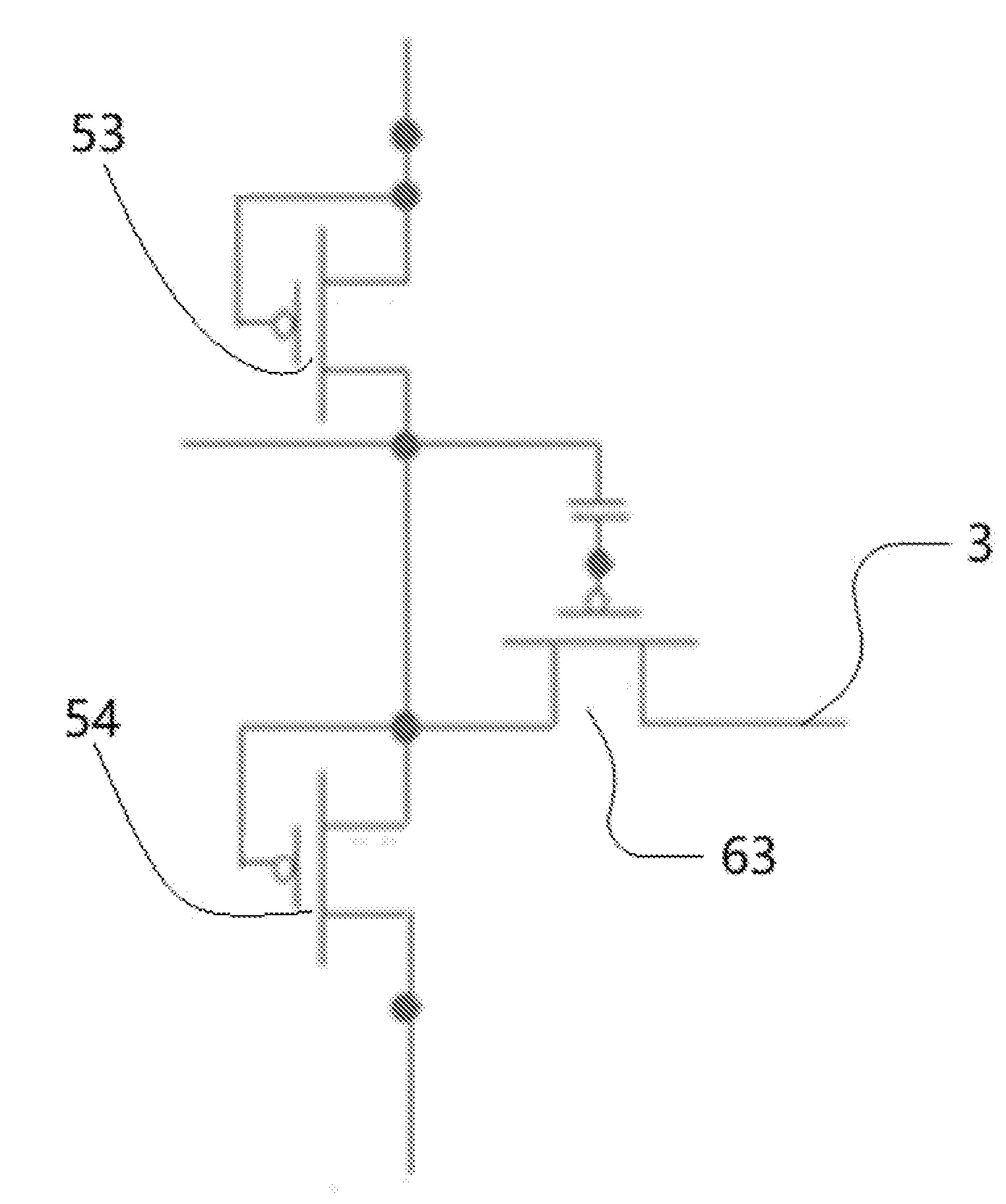
9. The display panel according to claim 6 wherein the third N-type thin film transistor and the fourth thin film transistor are N-type thin film transistors.
10. (canceled)
11. (canceled)
12. The display panel according to claim 2, wherein the first discharge circuit comprises a first N-type thin film transistor and a second N-type thin film transistor, a source of the first N-type thin film transistor is connected to the voltage gate high terminal, a gate of the first N-type thin film transistor is connected to a drain of the first N-type thin film transistor, and the gate and the drain of the first N-type thin film transistor are also connected to a source of the second N-type thin film transistor, the source of the second N-type thin film transistor is also connected to the electrostatic input end, a gate of the second N-type thin film transistor is connected to a drain of the second N-type thin film transistor, and the gate and the drain of the second N-type thin film transistor are also connected to the voltage gate low terminal; and the second discharge circuit comprises a third N-type thin film transistor, a capacitor and a fourth N-type thin film transistor, a source of the third N-type thin film transistor is connected to a gate of the first N-type thin film transistor, a drain of the third N-type thin film transistor is connected to the common voltage terminal, the common voltage terminal is connected to GND, a first end of the capacitor is connected to the electrostatic input end, a second end of the capacitor is connected to a gate of the third N-type thin film transistor, a source of the fourth N-type thin film transistor is connected to the second end of the capacitor, a gate of the fourth N-type thin film transistor is connected to the voltage gate high terminal, and a drain of the fourth N-type thin film transistor is connected to the voltage gate low terminal.
13. The display panel according to claim 2, wherein the first discharge circuit comprises a first P-type thin film transistor and a second P-type thin film transistor, a gate of the first P-type thin film transistor is connected to a drain of the first P-type thin film transistor, and the gate and the drain of the first P-type thin film transistor are also connected to the voltage gate high terminal, a source of the first P-type thin film transistor is connected to the electrostatic input end, a gate of the second P-type thin film transistor is connected to a drain of the second P-type thin film transistor, and the gate and the drain of the second P-type thin film transistor are also connected to the source of the first P-type thin film transistor, and a source of the second P-type thin film transistor is connected to the voltage gate low terminal; wherein the second discharge circuit comprises a third N-type thin film transistor, a capacitor and a fourth N-type thin film transistor, a source of the third N-type thin film transistor is connected to the gate of the first P-type thin film transistor, a drain of the third N-type thin film transistor is connected to the common voltage terminal, the common voltage terminal is connected to GND, a first end of the capacitor is connected to the electrostatic input end, a second end of the capacitor is connected to a gate of the third N-type thin film transistor, a source of the fourth N-type thin film transistor is connected to the second end of the capacitor, a gate of the fourth N-type thin film transistor is connected to the voltage gate high terminal, and a drain of the fourth N-type thin film transistor is connected to the voltage gate low terminal.
14. The display panel according to claim 2, wherein the first discharge circuit comprises a first P-type thin film transistor and a second P-type thin film transistor, a gate of the first P-type thin film transistor is connected to a drain of the first P-type thin film transistor, and the gate and the drain of the first P-type thin film transistor are also connected to the voltage gate high terminal, a source of the first P-type thin film transistor is connected to the electrostatic input end, a gate of the second P-type thin film transistor is connected to a drain of the second P-type thin film transistor, and the gate and the drain of the second P-type thin film transistor are also connected to the source of the first P-type thin film transistor, and a source of the second P-type thin film transistor is connected to the voltage gate low terminal, and the second discharge circuit comprises a third P-type thin film transistor, a capacitor and a fourth P-type thin film transistor, a source of the third P-type thin film transistor is connected to the gate of the second P-type thin film transistor, a drain of the third P-type thin film transistor is connected to the common voltage terminal, the common voltage terminal is connected to GND, a first end of the capacitor is connected to the electrostatic input end, a second end of the capacitor is connected to a gate of the third P-type thin film transistor, a source of the fourth P-type thin film transistor is connected to the second end of the capacitor, a gate of the fourth P-type thin film transistor is connected to the voltage gate low terminal, and a drain of the fourth P-type thin film transistor is connected to the voltage gate high terminal.
15. The display panel according to claim 2, wherein the display panel comprises a gate integrated circuit, and the voltage gate high terminal and the voltage gate low terminal are respectively connected at a thin film transistor voltage turn-on end and a thin film transistor voltage turn-off end of the gate integrated circuit.
16. (canceled)
17. (canceled)
18. (canceled)
19. (canceled)
20. (canceled)
21. A display device, comprising a display panel, comprising: a substrate including a plurality of pixel regions; and an electrostatic discharge circuit disposed on the substrate; wherein the electrostatic discharge circuit comprises a voltage gate high terminal, a voltage gate low terminal, an electrostatic input end and a common voltage terminal coupled with components of the display panel; and a first discharge circuit, wherein an output end of the first discharge circuit is connected to the voltage gate high terminal and the voltage gate low terminal respectively, a control end of the first discharge circuit is connected to the electrostatic input end, and an input end of the first discharge circuit is connected to the electrostatic input end; and a second discharge circuit, wherein an input end of the second discharge circuit is connected to the electrostatic input end, and an output end of the second discharge circuit is connected to the common voltage terminal.
22. The display device according to claim 21, wherein the second discharge circuit comprises a first conducting line with one end connected to the common voltage terminal, and the common voltage terminal is connected to GND.
23. The display device according to claim 21, wherein the second discharge circuit comprises a first conducting line with one end connected to the common voltage terminal, and the common voltage terminal is connected to a common voltage end of the display panel.
24. The display device according to claim 21, wherein the second discharge circuit comprises a third thin film transistor, an input end of the third thin film transistor is connected to the electrostatic input end, a control end of the third thin film transistor is connected to the electrostatic input end, and an output end of the third thin film transistor is connected to the common voltage terminal.
25. The display device according to claim 24, wherein the second discharge circuit comprises a capacitor, a first end of the capacitor is connected to the electrostatic input end, and a second end of the capacitor is connected to the control end of the third thin film transistor.
26. The display device according to claim 25, wherein the second discharge circuit comprises a fourth thin film transistor, an input end of a fourth thin film transistor is connected to the second end of the capacitor, a control end of the fourth thin film transistor is connected to the voltage gate high terminal, an output end of the fourth thin film transistor is connected to the voltage gate low terminal, an input end of a fourth thin film transistor is connected to the second end of the capacitor.
27. The display device according to claim 25, wherein the second discharge circuit comprises a fourth thin film transistor, an input end of a fourth thin film transistor is connected to the second end of the capacitor, a control end of the fourth thin film transistor is connected to the voltage gate low terminal, and an output end of the fourth thin film transistor is connected to the voltage gate high terminal.
Description
TECHNICAL FIELD
[0001] The present application relates to the technical field of displays, and particularly relates to a display panel.
BACKGROUND
[0002] Liquid crystal display apparatuses (LCD apparatuses) have numerous advantages, such as a thin body, power saving, no radiation, etc., and are widely used. Most liquid crystal display apparatuses in a current market are backlit liquid crystal display apparatuses, each including a liquid crystal panel and a backlight module. Working principle of the liquid crystal panel is that liquid crystals are put in two parallel glass substrates, and a driving voltage is applied to two glass substrates to control rotational direction of the liquid crystals, to refract light rays of the backlight module to generate a picture.
[0003] Thin film transistor liquid crystal display apparatuses (TFT-LCD apparatuses) currently maintain a leading status in the display field because of low power consumption, excellent picture quality, high production yield, and other properties. Similarly, the TFT-LCD apparatus includes a liquid crystal panel and a backlight module. The display panel includes a color filter substrate (CF substrate), a thin film transistor substrate (TFT substrate), a mask and transparent electrodes on relative inner sides of the above substrates. A layer of liquid crystals (LC) is positioned between two substrates.
[0004] However, for electrostatic discharge (ESD), if the ESD exceeds a certain voltage, then an integrated circuit chip medium is punctured, a chip wire is broken, leakage current is increased to accelerate aging, electric performance parameters are changed, and the like. Thus, protection for the ESD is very important.
SUMMARY
[0005] A technical problem to be solved by the present application is to provide a display panel having a reliable and effective protection circuit.
[0006] A purpose of the present application is realized through a technical solution as follows.
[0007] A display panel includes: a substrate including a plurality of pixel regions, and an electrostatic discharge circuit disposed on the substrate, where the electrostatic discharge circuit includes a voltage gate high terminal, a voltage gate low terminal, an electrostatic input end and a common voltage terminal coupled with components of the display panel, and a first discharge unit, where an output end of the first discharge unit is connected to the voltage gate high terminal and the voltage gate low terminal respectively and a control end and an input end of the first discharge unit are connected to the electrostatic input end, and a second discharge unit, where an input end of the second discharge unit is connected to the electrostatic input end, and an output end of the second discharge unit is connected to the common voltage terminal.
[0008] Optionally, the second discharge unit includes a first conducting line with one end connected to the common voltage terminal. The common voltage terminal is connected to GND. A line thickness required for a conducting line used between the voltage gate high terminal (VGH) and the voltage gate low terminal (VGL) is small. This is equivalent to a large resistor station. A relative leakage current is also small. A capability of the first discharge unit alone to perform current leakage is insufficient. However, the second conducting line is used for connection of a grounding end (GND). A line width of the second conducting line is greatly larger than line widths of VGH and VGL. Therefore, dischargeable current is greater than original current to achieve a better protection.
[0009] Optionally, the second discharge unit includes a first conducting line with one end connected to the common voltage terminal. The common voltage terminal is connected to a common voltage end of the display panel. A line thickness required for a conducting line used between the voltage gate high terminal (VGH) and the voltage gate low terminal (VGL) is small. This is equivalent to a large resistor station. A relative leakage current is also small. A capability of the first discharge unit alone to perform current leakage is insufficient. However, the second conducting line is used for connection of a common voltage end (VCOM). A line width of the second conducting line is greatly larger than line widths of VGH and VGL. Therefore, dischargeable current is greater than original current to achieve a better protection.
[0010] Optionally, the second discharge circuit includes a third thin film transistor. An input end of the third thin film transistor are connected to the electrostatic input end, a control end of the third thin film transistor are connected to the electrostatic input end. An output end of the third thin film transistor is connected to the common voltage terminal. The second discharge unit leaks current through the third thin film transistor, which is simple, effective and reliable in arrangement.
[0011] Optionally, the second discharge circuit includes a capacitor. A first end of the capacitor is connected to the electrostatic input end. A second end of the capacitor is connected to the control end of the third thin film transistor. Through characteristics of direct current blocking, alternating current conducting, high frequency conducting and low frequency blocking of the capacitor, when a voltage range is within VGL to VGH, the second discharge unit does not participate in the effect. Meanwhile, when the voltage range is not within VGL to VGH, for example, when a positive large voltage appears instantaneously, the second discharge unit can be properly operated without producing VGL current reserved by the second thin film transistor.
[0012] The second discharge circuit includes a fourth thin film transistor. An input end of a fourth thin film transistor is connected to the second end of the capacitor. A control end of the fourth thin film transistor is connected to the voltage gate high terminal. An output end of the fourth thin film transistor is connected to the voltage gate low terminal. Or, an input end of a fourth thin film transistor is connected to the second end of the capacitor. A control end of the fourth thin film transistor is connected to the voltage gate low terminal. An output end of the fourth thin film transistor is connected to the voltage gate high terminal. Conduction of the fourth thin film transistor further completes a discharge function of the second discharge unit. Meanwhile, a potential of the second end of the capacitor is pulled to be consistent with the common voltage terminal. Because of this, when the voltage range is within VGL to VGH, the third thin film transistor is not conducted to discharge to influence proper operation of the protection circuit.
[0013] Optionally, the first discharge circuit includes a first N-type thin film transistor and a second N-type thin film transistor. A source of the first N-type thin film transistor is connected to the voltage gate high terminal, a gate of the first N-type thin film transistor is connected to a drain of the first N-type thin film transistor, and the gate and the drain of the first N-type thin film transistor are also connected to a source of the second N-type thin film transistor. A source of the second N-type thin film transistor is also connected to the electrostatic input end. A gate of the second N-type thin film transistor is connected to a drain of the second N-type thin film transistor, and the gate and the drain of the second N-type thin film transistor are also connected to the voltage gate low terminal; and the second discharge circuit includes a third N-type thin film transistor, a capacitor and a fourth N-type thin film transistor. A source of the third N-type thin film transistor is connected to a gate of the first N-type thin film transistor. A drain of the third N-type thin film transistor is connected to the common voltage terminal. The common voltage terminal is connected to GND. A first end of the capacitor is connected to the electrostatic input end. A second end of the capacitor is connected to a gate of the third N-type thin film transistor. A source of the fourth N-type thin film transistor is connected to the second end of the capacitor. A gate of the fourth N-type thin film transistor is connected to the voltage gate high terminal. A drain of the fourth N-type thin film transistor is connected to the voltage gate low terminal. This is an embodiment of the protection circuit and defines specifically used electrical elements and connection relationships.
[0014] Optionally, the first discharge circuit includes a first P-type thin film transistor and a second P-type thin film transistor. A gate of the first P-type thin film transistor is connected to a drain of the first P-type thin film transistor, and the gate and the drain of the first P-type thin film transistor are also connected to the voltage gate high terminal. A source of the first P-type thin film transistor is connected to the electrostatic input end. A gate of the second P-type thin film transistor is connected to a drain of the second P-type thin film transistor, and the gate and the drain of the second P-type thin film transistor are also connected to the source of the first P-type thin film transistor. A source of the second P-type thin film transistor is connected to the voltage gate low terminal; and the second discharge circuit includes a third N-type thin film transistor, a capacitor and a fourth N-type thin film transistor. A source of the third N-type thin film transistor is connected to a gate of the first N-type thin film transistor. A drain of the third N-type thin film transistor is connected to the common voltage terminal. The common voltage terminal is connected to GND. A first end of the capacitor is connected to the electrostatic input end. A second end of the capacitor is connected to a gate of the third N-type thin film transistor. A source of the fourth N-type thin film transistor is connected to the second end of the capacitor. A gate of the fourth N-type thin film transistor is connected to the voltage gate high terminal. A drain of the fourth N-type thin film transistor is connected to the voltage gate low terminal. This is an embodiment of the protection circuit and defines specifically used electrical elements and connection relationships.
[0015] Optionally, the first discharge circuit includes a first P-type thin film transistor and a second P-type thin film transistor. A gate of the first P-type thin film transistor is connected to a drain of the first P-type thin film transistor, and the gate and the drain of the first P-type thin film transistor are also connected to the voltage gate high terminal. A source of the first P-type thin film transistor is connected to the electrostatic input end. A gate of the second P-type thin film transistor is connected to a drain of the second P-type thin film transistor, and the gate and the drain of the second P-type thin film transistor are also connected to the source of the first P-type thin film transistor. A source of the second P-type thin film transistor is connected to the voltage gate low terminal; and the second discharge circuit includes a third P-type thin film transistor, a capacitor and a fourth P-type thin film transistor. A source of the third P-type thin film transistor is connected to a gate of the second P-type thin film transistor. A drain of the third P-type thin film transistor is connected to the common voltage terminal. The common voltage terminal is connected to GND. A first end of the capacitor is connected to the electrostatic input end. A second end of the capacitor is connected to a gate of the third P-type thin film transistor. A source of the fourth P-type thin film transistor is connected to the second end of the capacitor. A gate of the fourth P-type thin film transistor is connected to the voltage gate low terminal. A drain of the fourth P-type thin film transistor is connected to the voltage gate high terminal. This is an embodiment of the protection circuit and defines specifically used electrical elements and connection relationships.
[0016] The display panel includes a gate integrated circuit. The voltage gate high terminal and the voltage gate low terminal are respectively connected at a thin film transistor voltage turn-on end and a thin film transistor voltage turn-off end of the gate integrated circuit. This is specific connection of VGH and VGL.
[0017] In the present application, since the connected first discharge unit and second discharge unit act jointly and the other end of the second discharge unit is connected to the common voltage terminal, an ESD current path is increased, and speed and number of leakage current are increased, thereby realizing a better protection for the display panel and prolonging service life.
BRIEF DESCRIPTION OF DRAWINGS
[0018] The drawings included are used for providing further understanding of embodiments of the present application, constitute portion of the description, and are used to illustrate implementation manners of the present application, and interpret principles of the present application together with text description. Apparently, the drawings in the following description are merely some embodiments of the present application, and for those of ordinary skill in the art, other drawings can also be obtained according to the drawings without contributing creative labor. In the drawings:
[0019] FIG. 1 is a schematic diagram of a protection circuit of a display panel in an embodiment of the present application.
[0020] FIG. 2 is a schematic diagram of a protection circuit of a display panel in an embodiment of the present application.
[0021] FIG. 3 is a schematic diagram of a protection circuit of a display panel in an embodiment of the present application.
[0022] FIG. 4 is a schematic diagram of a protection circuit of a display panel in an embodiment of the present application.
[0023] FIG. 5 is a schematic diagram of a protection circuit of a display panel in an embodiment of the present application.
[0024] FIG. 6 is a schematic diagram of a protection circuit of a display panel in an embodiment of the present application.
[0025] FIG. 7 is a schematic diagram of a protection circuit of a display panel in an embodiment of the present application.
[0026] FIG. 8 is a schematic diagram of a protection circuit of a display panel in an embodiment of the present application.
[0027] FIG. 9 is a structural schematic diagram of a display panel in an embodiment of the present application.
DETAILED DESCRIPTION
[0028] Specific structure and function details disclosed herein are only representative and are used for the purpose of describing exemplary embodiments of the present application. However, the present application may be specifically achieved in many alternative forms and shall not be interpreted to be only limited to the embodiments described herein.
[0029] It should be understood in the description of the present application that terms such as "central", "horizontal", "upper", "lower", "left", "right", "vertical", "horizontal", "top", "bottom", "inner", "outer", etc. indicate direction or position relationships shown based on the drawings, and are only intended to facilitate the description of the present application and the simplification of the description rather than to indicate or imply that the indicated device or element must have a specific direction or constructed and operated in a specific direction, and therefore, shall not be understood as a limitation to the present application. In addition, the terms such as "first" and "second" are only used for the purpose of description, rather than being understood to indicate or imply relative importance or hint the number of indicated technical features. Thus, the feature limited by "first" and "second" can explicitly or impliedly include one or more features. In the description of the present application, the meaning of "a plurality of" is two or more unless otherwise specified. In addition, the term "comprise" and any variant are intended to cover non-exclusive inclusion.
[0030] It should be noted in the description of the present application that, unless otherwise specifically regulated and defined, terms such as "installation," "connected," and "connection" shall be understood in broad sense, and for example, may refer to fixed connection or detachable connection or integral connection, may refer to mechanical connection or electrical connection, and may refer to direct connection or indirect connection through an intermediate medium or inner communication of two elements. For those of ordinary skill in the art, the meanings of the above terms in the present application may be understood according to concrete conditions.
[0031] The terms used herein are intended to merely describe specific embodiments, not to limit the exemplary embodiments. Unless otherwise noted clearly in the context, singular forms "one" and "single" used herein are also intended to comprise plurals. It should also be understood that the terms "comprise" and/or "include" used herein specify the existence of stated features, integers, steps, operation, units and/or assemblies, not excluding the existence or addition of one or more other features, integers, steps, operation, units, assemblies and/or combinations of these.
[0032] The present application will be further described in detail below in combination with the drawings and optional embodiments.
[0033] In one or more embodiments of the present application, as shown in FIGS. 1 to 2, the display panel includes: a substrate including a plurality of pixel regions and an electrostatic discharge unit disposed on the substrate and including a voltage gate high terminal, a voltage gate low terminal, an electrostatic input end and a common voltage terminal coupled with components of the display panel; and a first discharge unit, where an output end of the first discharge unit is respectively connected to the voltage gate high terminal and the voltage gate low terminal, and a control end and an input end of the first discharge unit are connected to the electrostatic input end; and a second discharge unit, where an input end of the second discharge unit is connected to the electrostatic input end, and an output end of the second discharge unit is connected to the common voltage terminal. The first discharge circuit includes a first thin film transistor and a second thin film transistor. An output end of the first thin film transistor is connected to the voltage gate high terminal. An input end of the first thin film transistor and an output end of the second thin film transistor are connected to the electrostatic input end. An input end of the second thin film transistor is connected to the voltage gate low terminal. In the present application, since the connected first discharge unit and second discharge unit act jointly and the other end of the second discharge unit is connected to the common voltage terminal, an ESD current path is increased, and speed and number of leakage current are increased, thereby realizing a better protection for the display panel and prolonging service life. As shown in FIG. 9, an ESD circuit, a gate driving circuit and a source driving circuit are disposed on the substrate. The horizontally disposed scanning lines and the vertically disposed data lines are coupled with corresponding circuits. The plurality of data lines and the plurality of scanning lines are successively disposed to be intersected to form a plurality of pixel regions.
[0034] Specifically, the second discharge unit includes a first conducting line with one end connected to the common voltage terminal. The common voltage terminal is connected to GND. A line thickness required for a conducting line used between the voltage gate high terminal (VGH) and the voltage gate low terminal (VGL) is small. This is equivalent to a large resistor station. A relative leakage current is also small. A capability of the first discharge unit alone to perform current leakage is insufficient. However, the second conducting line is connected to the ground (GND). A line width of the second conducting line is greatly larger than line widths of VGH and VGL. Therefore, dischargeable current is greater than original current to achieve a better protection. The second discharge unit includes a first conducting line with one end connected to the common voltage terminal. The common voltage terminal is connected to a common voltage end of the display panel. However, the second conducting line is connected to the common voltage (VCOM). A line width of the second conducting line is greatly larger than line widths of VGH and VGL. Therefore, dischargeable current is greater than original current to achieve a better protection. The display panel includes a gate integrated circuit. The voltage gate high terminal and the voltage gate low terminal are respectively connected at a thin film transistor voltage turn-on end and a thin film transistor voltage turn-off end of the gate integrated circuit.
[0035] In one or more embodiments, the display panel comprises: a substrate including a plurality of pixel regions, and an electrostatic discharge circuit disposed on the substrate and including a voltage gate high terminal, a voltage gate low terminal, an electrostatic input end and a common voltage terminal coupled with components of the display panel; and a first discharge unit, where an output end of the first discharge unit is respectively connected to the voltage gate high terminal and the voltage gate low terminal, and a control end and an input end of the first discharge unit are connected to the electrostatic input end; and a second discharge unit, where an input end of the second discharge unit is connected to the electrostatic input end, and an output end of the second discharge unit is connected to the common voltage terminal. The first discharge circuit comprises a first thin film transistor and a second thin film transistor. An output end of the first thin film transistor is connected to the voltage gate high terminal. An input end of the first thin film transistor and an output end of the second thin film transistor are connected to the electrostatic input end. An input end of the second thin film transistor is connected to the voltage gate low terminal. Since the connected first discharge unit and second discharge unit act jointly and the other end of the second discharge unit is connected to the common voltage terminal, an ESD current path is increased, and speed and number of leakage current are increased, thereby realizing a better protection for the display panel and prolonging service life. The second discharge circuit comprises a third thin film transistor and a capacitor. An input end of the third thin film transistor are connected to the electrostatic input end. A control end of the third thin film transistor are connected to the electrostatic input end. An output end of the third thin film transistor is connected to the common voltage terminal. The second discharge unit leaks current through the third thin film transistor, which is simple, effective and reliable in arrangement. A first end of the capacitor is connected to the electrostatic input end. A second end of the capacitor is connected to the control end of the third thin film transistor. Through characteristics of direct current blocking, alternating current conducting, high frequency conducting and low frequency blocking of the capacitor, when a voltage range is within VGL to VGH, the second discharge unit does not participate in the effect. Meanwhile, when the voltage range is not within VGL to VGH, for example, when a positive large voltage appears instantaneously, the second discharge unit can be properly operated without producing VGL current reserved by the second thin film transistor. Therefore, if an input voltage range of PIN (PIN as the pin of the electrostatic input end) is within VGL to VGH, because a capacitor can be regarded as an open circuit in direct current, the capacitor and the thin film transistor do not act.
[0036] Specifically, as shown in FIG. 3, the first thin film transistor and the second thin film transistor are N-type thin film transistors: a first N-type thin film transistor and a second N-type thin film transistor. A source of the first N-type thin film transistor is connected to the voltage gate high terminal. A gate of the first N-type thin film transistor is connected to a drain of the first N-type thin film transistor, and the gate and the drain of the first N-type thin film transistor are also connected to a source of the second N-type thin film transistor. A source of the second N-type thin film transistor is also connected to the electrostatic input end. A gate of the second N-type thin film transistor is connected to a drain of the second N-type thin film transistor, and the gate and the drain of the second N-type thin film transistor are also connected to the voltage gate low terminal. A source of the third N-type thin film transistor is connected to a gate of the first N-type thin film transistor. A drain of the third N-type thin film transistor is connected to the common voltage terminal. The common voltage terminal is connected to GND. A first end of the capacitor is connected to the electrostatic input end. A second end of the capacitor is connected to a gate of the third N-type thin film transistor.
[0037] When a positive large voltage instantaneously comes in the PIN, the first N-type thin film transistor is conducted and first discharge current is generated. Since the potential of the PIN is increased instantaneously and a potential of a connection point between the second end of the capacitor and the gate of the third N-type thin film transistor is simultaneously increased under a special efficacy of capacitive coupling, the third N-type thin film transistor is also conducted. At this moment, the positive large voltage of the PIN can leak current to GND. Since wiring of GND is usually thicker than wiring of VGL, a corresponding resistance value is greatly smaller than a resistance value of VGL and the second discharge current is greater than the first discharge current.
[0038] Of course, the first discharge unit can use a P-type thin film transistor, or use the N-type thin film transistor and the P-type thin film transistor together. For example, the first thin film transistor and the second thin film transistor are P-type thin film transistors: a first P-type thin film transistor and a second P-type thin film transistor. A gate of the first P-type thin film transistor is connected to a drain of the first P-type thin film transistor, and the gate and the drain of the first P-type thin film transistor are also connected to the voltage gate high terminal. A source of the first P-type thin film transistor is connected to the electrostatic input end. A gate of the second P-type thin film transistor is connected to a drain of the second P-type thin film transistor, and the gate and the drain of the second P-type thin film transistor are also connected to the source of the first P-type thin film transistor. A source of the second P-type thin film transistor is connected to the voltage gate low terminal.
[0039] In one or more embodiments, the display panel comprises: a substrate including a plurality of pixel regions, and an electrostatic discharge circuit disposed on the substrate and including a voltage gate high terminal, a voltage gate low terminal, an electrostatic input end and a common voltage terminal coupled with components of the display panel; and a first discharge unit, where an output end of the first discharge unit is respectively connected to the voltage gate high terminal and the voltage gate low terminal, and a control end and an input end of the first discharge unit are connected to the electrostatic input end; and a second discharge unit, where an input end of the second discharge unit is connected to the electrostatic input end, and an output end of the second discharge unit is connected to the common voltage terminal. The first discharge unit comprises a first thin film transistor and a second thin film transistor. An output end of the first thin film transistor is connected to the voltage gate high terminal. An input end of the first thin film transistor and an output end of the second thin film transistor are connected to the electrostatic input end. An input end of the second thin film transistor is connected to the voltage gate low terminal. Since the connected first discharge unit and second discharge unit act jointly and the other end of the second discharge unit is connected to the common voltage terminal, an ESD current path is increased, and speed and number of leakage current are increased, thereby realizing a better protection for the display panel and prolonging service life. The second discharge circuit comprises a third thin film transistor, a capacitor and a fourth thin film transistor. An input end of the third thin film transistor are connected to the electrostatic input end. A control end of the third thin film transistor are connected to the electrostatic input end. An output end of the third thin film transistor is connected to the common voltage terminal. The second discharge unit leaks current through the third thin film transistor, which is simple, effective and reliable in arrangement. A first end of the capacitor is connected to the electrostatic input end. A second end of the capacitor is connected to the control end of the third thin film transistor. Through characteristics of direct current blocking, alternating current conducting, high frequency conducting and low frequency blocking of the capacitor, when a voltage range is within VGL to VGH, the second discharge unit does not participate in the effect. Meanwhile, when the voltage range is not within VGL to VGH, for example, when a positive large voltage appears instantaneously, the second discharge unit can be properly operated without producing VGL current reserved by the second thin film transistor. Therefore, if an input voltage range of PIN is within VGL to VGH, because a capacitor can be regarded as an open circuit in direct current, the capacitor and the thin film transistor do not act. An input end of a fourth thin film transistor is connected to the second end of the capacitor. A control end of the fourth thin film transistor is connected to the voltage gate high terminal. An output end of the fourth thin film transistor is connected to the voltage gate low terminal; or an input end of a fourth thin film transistor is connected to the second end of the capacitor. A control end of the fourth thin film transistor is connected to the voltage gate low terminal. An output end of the fourth thin film transistor is connected to the voltage gate high terminal. Conduction of the fourth thin film transistor further completes a discharge function of the second discharge unit. Meanwhile, a potential of the second end of the capacitor is pulled to be consistent with the common voltage terminal. Because of this, when the voltage range is within VGL to VGH, the third thin film transistor is not conducted to discharge to influence proper operation of the protection circuit.
[0040] Specifically, as shown in FIGS. 4 to 5, FIG. 5 can be regarded as an actual equivalent circuit of FIG. 4. The first thin film transistor and the second thin film transistor are N-type thin film transistors: a first N-type thin film transistor and a second N-type thin film transistor. A source of the first N-type thin film transistor is connected to the voltage gate high terminal. A gate of the first N-type thin film transistor is connected to a drain of the first N-type thin film transistor, and the gate and the drain of the first N-type thin film transistor are also connected to a source of the second N-type thin film transistor. A source of the second N-type thin film transistor is also connected to the electrostatic input end. A gate of the second N-type thin film transistor is connected to a drain of the second N-type thin film transistor, and the gate and the drain of the second N-type thin film transistor are also connected to the voltage gate low terminal. The second discharge circuit includes a third N-type thin film transistor, a capacitor and a fourth N-type thin film transistor. A source of the third N-type thin film transistor is connected to a gate of the first N-type thin film transistor. A drain of the third N-type thin film transistor is connected to the common voltage terminal. The common voltage terminal is connected to GND. A first end of the capacitor is connected to the electrostatic input end. A second end of the capacitor is connected to a gate of the third N-type thin film transistor. A source of the fourth N-type thin film transistor is connected to the second end of the capacitor. A gate of the fourth N-type thin film transistor is connected to the voltage gate high terminal. A drain of the fourth N-type thin film transistor is connected to the voltage gate low terminal. This is an embodiment of the protection circuit and defines specifically used electrical elements and connection relationships. Since the potential of the PIN is increased instantaneously and a potential of a connection point between the second end of the capacitor and the gate of the third N-type thin film transistor is simultaneously increased under a special efficacy of capacitive coupling, the third N-type thin film transistor is also conducted. At this moment, the positive large voltage of the PIN can leak current to GND. Since wiring of GND is usually thicker than wiring of VGL, a corresponding resistance value is greatly smaller than a resistance value of VGL and the second discharge current is greater than the first discharge current. However, the fourth N-type thin film transistor also simultaneously pulls the potential of a connection point between the second end of the capacitor and the gate of the third N-type thin film transistor to GND. Therefore, when a positive large voltage instantaneously comes in the PIN, the leaked current is a sum of the first discharge current, the second discharge current and the third discharge current. Compared with an individual action of the first discharge unit, a total leakage current is larger and a better protection is realized.
[0041] Of course, the first discharge unit can use a P-type thin film transistor, or use the N-type thin film transistor and the P-type thin film transistor together. For example, the first thin film transistor and the second thin film transistor are P-type thin film transistors: a first P-type thin film transistor and a second P-type thin film transistor. A gate of the first P-type thin film transistor is connected to a drain of the first P-type thin film transistor, and the gate and the drain of the first P-type thin film transistor are also connected to the voltage gate high terminal. A source of the first P-type thin film transistor is connected to the electrostatic input end. A gate of the second P-type thin film transistor is connected to a drain of the second P-type thin film transistor, and the gate and the drain of the second P-type thin film transistor are also connected to the source of the first P-type thin film transistor. A source of the second P-type thin film transistor is connected to the voltage gate low terminal.
[0042] In one or more embodiments, as shown in FIG. 2, the display panel comprises: a substrate including a plurality of pixel regions, and an electrostatic discharge circuit disposed on the substrate and including a voltage gate high terminal, a voltage gate low terminal, an electrostatic input end and a common voltage terminal coupled with components of the display panel; and a first discharge unit, where the first discharge unit include a first P-type thin film transistor and a second P-type thin film transistor, a gate of the first P-type thin film transistor is connected to a drain of the first P-type thin film transistor, the gate and the drain of the first P-type thin film transistor are also connected to the voltage gate high terminal, a source of the first P-type thin film transistor is connected to the electrostatic input end, a gate of the second P-type thin film transistor is connected to a drain of the second P-type thin film transistor, the gate and the drain of the second P-type thin film transistor are also connected to the source of the first P-type thin film transistor, and a source of the second P-type thin film transistor is connected to the voltage gate low terminal; and a second discharge unit, where an input end of the second discharge unit is connected to the electrostatic input end, and an output end of the second discharge unit is connected to the common voltage terminal. In the present application, since the connected first discharge unit and second discharge unit act jointly and the other end of the second discharge unit is connected to the common voltage terminal, an ESD current path is increased, and speed and number of leakage current are increased, thereby realizing a better protection for the display panel and prolonging service life.
[0043] Specifically, the second discharge unit comprises a first conducting line with one end connected to the common voltage terminal. The common voltage terminal is connected to GND. A line thickness required for a conducting line used between the voltage gate high terminal (VGH) and the voltage gate low terminal (VGL) is small. This is equivalent to a large resistor station. A relative leakage current is also small. A capability of the first discharge unit alone to perform current leakage is insufficient. However, the second conducting line is used for connection of a grounding end (GND). A line width of the second conducting line is greatly larger than line widths of VGH and VGL. Therefore, dischargeable current is greater than original current to achieve a better protection. The second discharge unit comprises a first conducting line with one end connected to the common voltage terminal. The common voltage terminal is connected to a common voltage end of the display panel. However, the second conducting line is used for connection of a common voltage end (VCOM). A line width of the second conducting line is greatly larger than line widths of VGH and VGL. Therefore, dischargeable current is greater than original current to achieve a better protection. The display panel comprises a gate integrated circuit. The voltage gate high terminal and the voltage gate low terminal are respectively connected at a thin film transistor voltage turn-on end and a thin film transistor voltage turn-off end of the gate integrated circuit.
[0044] In one or more embodiments, the display panel comprises: a substrate including a plurality of pixel regions, and an electrostatic discharge circuit disposed on the substrate and including a voltage gate high terminal, a voltage gate low terminal, an electrostatic input end and a common voltage terminal coupled with components of the display panel; and a first discharge unit, where the first discharge unit comprises a first P-type thin film transistor and a second P-type thin film transistor, a gate of the first P-type thin film transistor is connected to a drain of the first P-type thin film transistor, the gate and the drain of the first P-type thin film transistor are also connected to the voltage gate high terminal, a source of the first P-type thin film transistor is connected to the electrostatic input end, a gate of the second P-type thin film transistor is connected to a drain of the second P-type thin film transistor, the gate and the drain of the second P-type thin film transistor are also connected to the source of the first P-type thin film transistor, and a source of the second P-type thin film transistor is connected to the voltage gate low terminal; and a second discharge unit, where an input end of the second discharge unit is connected to the electrostatic input end, and an output end of the second discharge unit is connected to the common voltage terminal. Since the connected first discharge unit and second discharge unit act jointly and the other end of the second discharge unit is connected to the common voltage terminal, an ESD current path is increased, and speed and number of leakage current are increased, thereby realizing a better protection for the display panel and prolonging service life. The second discharge circuit include a third thin film transistor and a capacitor. An input end of the third thin film transistor are connected to the electrostatic input end. A control end of the third thin film transistor are connected to the electrostatic input end. An output end of the third thin film transistor is connected to the common voltage terminal. The second discharge unit leaks current through the third thin film transistor, which is simple, effective and reliable in arrangement. The second discharge circuit comprises: A first end of the capacitor is connected to the electrostatic input end, and a second end of the capacitor is connected to the control end of the third thin film transistor. Through characteristics of direct current blocking, alternating current conducting, high frequency conducting and low frequency blocking of the capacitor, when a voltage range is within VGL to VGH, the second discharge unit does not participate in the effect. Meanwhile, when the voltage range is not within VGL to VGH, for example, when a positive large voltage appears instantaneously, the second discharge unit can be properly operated without producing VGL current reserved by the second thin film transistor. Therefore, if an input voltage range of PIN is within VGL to VGH, because a capacitor can be regarded as an open circuit in direct current, the capacitor and the thin film transistor do not act.
[0045] Specifically, as shown in FIG. 6, the third thin film transistor is a P-type thin film transistor: a third P-type thin film transistor. A source of the third P-type thin film transistor is connected to a gate of the second P-type thin film transistor. A drain of the third P-type thin film transistor is connected to the common voltage terminal. The common voltage terminal is connected to GND. A first end of the capacitor is connected to the electrostatic input end. A second end of the capacitor is connected to a gate of the third P-type thin film transistor. Since the potential of the PIN is increased instantaneously and a potential of a connection point between the second end of the capacitor and the gate of the third N-type thin film transistor is simultaneously increased under a special efficacy of capacitive coupling, the third N-type thin film transistor is also conducted. At this moment, the positive large voltage of the PIN can leak current to GND. Since wiring of GND is usually thicker than wiring of VGL, a corresponding resistance value is greatly smaller than a resistance value of VGL and the second discharge current is greater than the first discharge current.
[0046] In one or more embodiments, the display panel comprises: a substrate including a plurality of pixel regions, and an electrostatic discharge circuit disposed on the substrate and including a voltage gate high terminal, a voltage gate low terminal, an electrostatic input end and a common voltage terminal coupled with components of the display panel; and a first discharge unit, where the first discharge unit comprises a first P-type thin film transistor and a second P-type thin film transistor, a gate of the first P-type thin film transistor is connected to a drain of the first P-type thin film transistor, the gate and the drain of the first P-type thin film transistor are also connected to the voltage gate high terminal, a source of the first P-type thin film transistor is connected to the electrostatic input end, a gate of the second P-type thin film transistor is connected to a drain of the second P-type thin film transistor, the gate and the drain of the second P-type thin film transistor are also connected to the source of the first P-type thin film transistor, and a source of the second P-type thin film transistor is connected to the voltage gate low terminal; and a second discharge unit, where an input end of the second discharge unit is connected to the electrostatic input end, and an output end of the second discharge unit is connected to the common voltage terminal. Since the connected first discharge unit and second discharge unit act jointly and the other end of the second discharge unit is connected to the common voltage terminal, an ESD current path is increased, and speed and number of leakage current are increased, thereby realizing a better protection for the display panel and prolonging service life. The second discharge circuit includes a third thin film transistor, a capacitor and a fourth thin film transistor. An input end of the third thin film transistor are connected to the electrostatic input end. A control end of the third thin film transistor are connected to the electrostatic input end. An output end of the third thin film transistor is connected to the common voltage terminal. The second discharge unit leaks current through the third thin film transistor, which is simple, effective and reliable in arrangement. The second discharge circuit includes: A first end of the capacitor is connected to the electrostatic input end, and a second end of the capacitor is connected to the control end of the third thin film transistor. Through characteristics of direct current blocking, alternating current conducting, high frequency conducting and low frequency blocking of the capacitor, when a voltage range is within VGL to VGH, the second discharge unit does not participate in the effect. Meanwhile, when the voltage range is not within VGL to VGH, for example, when a positive large voltage appears instantaneously, the second discharge unit can be properly operated without producing VGL current reserved by the second thin film transistor. Therefore, if an input voltage range of PIN is within VGL to VGH, because a capacitor can be regarded as an open circuit in direct current, the capacitor and the thin film transistor do not act. A control end of the fourth thin film transistor is connected to the voltage gate low terminal. An output end of the fourth thin film transistor is connected to the voltage gate high terminal. Conduction of the fourth thin film transistor further completes a discharge function of the second discharge unit. Meanwhile, a potential of the second end of the capacitor is pulled to be consistent with the common voltage terminal. Because of this, when the voltage range is within VGL to VGH, the third thin film transistor is not conducted to discharge to influence proper operation of the protection circuit.
[0047] Specifically, as shown in FIGS. 7 to 8, FIG. 8 can be regarded as an actual equivalent circuit of FIG. 7. The third thin film transistor and the fourth thin film transistor are P-type thin film transistors: a third P-type thin film transistor and a fourth P-type thin film transistor. A source of the third P-type thin film transistor is connected to a gate of the second P-type thin film transistor. A drain of the third P-type thin film transistor is connected to the common voltage terminal. The common voltage terminal is connected to GND. A first end of the capacitor is connected to the electrostatic input end. A second end of the capacitor is connected to a gate of the third P-type thin film transistor. A source of the fourth P-type thin film transistor is connected to the second end of the capacitor. A gate of the fourth P-type thin film transistor is connected to the voltage gate low terminal. A drain of the fourth P-type thin film transistor is connected to the voltage gate high terminal. Since the potential of the PIN is increased instantaneously and a potential of a connection point between the second end of the capacitor and the gate of the third N-type thin film transistor is simultaneously increased under a special efficacy of capacitive coupling, the third N-type thin film transistor is also conducted. At this moment, the positive large voltage of the PIN can leak current to GND. Since wiring of GND is usually thicker than wiring of VGL, a corresponding resistance value is greatly smaller than a resistance value of VGL and the second discharge current is greater than the first discharge current. However, the fourth N-type thin film transistor also simultaneously pulls the potential of a connection point between the second end of the capacitor and the gate of the third N-type thin film transistor to GND. Therefore, when a positive large voltage instantaneously comes in the PIN, the leaked current is a sum of the first discharge current, the second discharge current and the third discharge current. Compared with an individual action of the first discharge unit, a total leakage current is larger and a better protection is realized.
[0048] In one or more embodiments, the present application further discloses a display device include a backlight module and the above display panel.
[0049] It should be noted that the substrate can be made of glass, plastics, etc. in the above embodiment.
[0050] In the above embodiment, the display panel includes a liquid crystal panel, an organic light-emitting diode (OLED) panel, a curved surface type panel, a plasma panel and the like. By taking the liquid crystal panel as an example, the liquid crystal panel includes a thin film transistor substrate (TFT Substrate) and a color filter substrate (CF Substrate). The TFT substrate and the CF substrate are disposed opposite to each other. Liquid crystals and photo spacers (PS) are disposed between the TFT substrate and the CF substrate. A thin film transistor (TFT) is disposed on the TFT substrate. A color filter layer is disposed on the CF substrate.
[0051] In the above embodiment, the CF substrate may include a TFT array. A color filter and the TFT array may be formed on the same substrate. The TFT substrate may include the color filter layer.
[0052] In the above embodiment, the display panel of the present application may be a curved surface type panel.
[0053] The above contents are further detailed descriptions of the present application in combination with specific optional embodiments. However, the specific implementation of the present application shall not be considered to be only limited to these descriptions. For those of ordinary skill in the art to which the present application belongs, several simple deductions or replacements may be made without departing from the conception of the present application, all of which shall be considered to belong to the protection scope of the present application.
* * * * *
D00000
D00001
D00002
D00003
D00004
D00005
D00006
D00007
D00008
D00009
XML
uspto.report is an independent third-party trademark research tool that is not affiliated, endorsed, or sponsored by the United States Patent and Trademark Office (USPTO) or any other governmental organization. The information provided by uspto.report is based on publicly available data at the time of writing and is intended for informational purposes only.
While we strive to provide accurate and up-to-date information, we do not guarantee the accuracy, completeness, reliability, or suitability of the information displayed on this site. The use of this site is at your own risk. Any reliance you place on such information is therefore strictly at your own risk.
All official trademark data, including owner information, should be verified by visiting the official USPTO website at www.uspto.gov. This site is not intended to replace professional legal advice and should not be used as a substitute for consulting with a legal professional who is knowledgeable about trademark law.