Light Wavelength Conversion Member And Light Emission Device
MOTEKI; Jun ; et al.
U.S. patent application number 16/328161 was filed with the patent office on 2019-06-27 for light wavelength conversion member and light emission device. This patent application is currently assigned to NGK SPARK PLUG CO., LTD.. The applicant listed for this patent is NGK SPARK PLUG CO., LTD.. Invention is credited to Tsuneyuki ITO, Yusuke KATSU, Takeshi MITSUOKA, Jun MOTEKI, Shohei TAKAKU.
| Application Number | 20190198726 16/328161 |
| Document ID | / |
| Family ID | 62150465 |
| Filed Date | 2019-06-27 |
| United States Patent Application | 20190198726 |
| Kind Code | A1 |
| MOTEKI; Jun ; et al. | June 27, 2019 |
LIGHT WAVELENGTH CONVERSION MEMBER AND LIGHT EMISSION DEVICE
Abstract
An optical wavelength conversion member including a polycrystalline ceramic sintered body containing, as main components, Al.sub.2O.sub.3 crystal grains and crystal grains of a component represented by formula A.sub.3B.sub.5O.sub.12:Ce, wherein A is at least one element selected from Sc, Y and lanthanoids (except for Ce), and B is at least one element selected from Al and Ga. Further, the following relations are satisfied: 0%.ltoreq.X.ltoreq.25%, 9%.ltoreq.Y.ltoreq.45%, and 48%.ltoreq.Z.ltoreq.90%, wherein X represents a proportion corresponding to the ratio a/N, Y represents a proportion corresponding to the ratio b/N, and Z represents a proportion corresponding to the ratio c/N and a, b, c and N are as defined herein. Also disclosed is a light-emitting device including the optical wavelength conversion member.
| Inventors: | MOTEKI; Jun; (Seto-shi, Aichi, JP) ; TAKAKU; Shohei; (Komaki-shi, Aichi, JP) ; KATSU; Yusuke; (Komaki-shi, Aichi, JP) ; MITSUOKA; Takeshi; (Konan-shi, Aichi, JP) ; ITO; Tsuneyuki; (Niwa-gun, Aichi, JP) | ||||||||||
| Applicant: |
|
||||||||||
|---|---|---|---|---|---|---|---|---|---|---|---|
| Assignee: | NGK SPARK PLUG CO., LTD. Nagoya-shi, Aichi JP |
||||||||||
| Family ID: | 62150465 | ||||||||||
| Appl. No.: | 16/328161 | ||||||||||
| Filed: | October 18, 2017 | ||||||||||
| PCT Filed: | October 18, 2017 | ||||||||||
| PCT NO: | PCT/JP2017/037679 | ||||||||||
| 371 Date: | February 25, 2019 |
| Current U.S. Class: | 1/1 |
| Current CPC Class: | C09K 11/7774 20130101; C04B 2235/3229 20130101; C04B 35/44 20130101; C04B 2235/5436 20130101; H01L 33/502 20130101; C04B 35/115 20130101; C04B 35/117 20130101; C04B 2235/3225 20130101; C04B 2235/96 20130101; H01L 33/505 20130101; C04B 2235/3224 20130101; C04B 2235/3222 20130101; H01L 33/50 20130101; H01L 33/507 20130101; C04B 2235/9646 20130101; C04B 2235/9661 20130101; C04B 2235/785 20130101; C04B 2235/3217 20130101; G02B 5/20 20130101; C04B 2235/5445 20130101; C04B 2235/786 20130101; C04B 2235/6567 20130101; H01L 33/501 20130101; H01L 33/16 20130101; H01L 33/504 20130101 |
| International Class: | H01L 33/50 20060101 H01L033/50; H01L 33/16 20060101 H01L033/16; C04B 35/44 20060101 C04B035/44; C04B 35/115 20060101 C04B035/115; C04B 35/117 20060101 C04B035/117; C09K 11/77 20060101 C09K011/77 |
Foreign Application Data
| Date | Code | Application Number |
|---|---|---|
| Oct 28, 2016 | JP | 2016-211843 |
| Oct 12, 2017 | JP | 2017-198555 |
Claims
1. An optical wavelength conversion member comprising a polycrystalline ceramic sintered body containing, as main components, Al.sub.2O.sub.3 crystal grains and crystal grains of a component represented by formula A.sub.3B.sub.5O.sub.12:Ce, the optical wavelength conversion member being characterized in that: each of A and B of the A.sub.3B.sub.5O.sub.12 is at least one element selected from the following element groups: A: Sc, Y, and lanthanoids (except for Ce), and B: Al and Ga; and the following relations are satisfied: 0%.ltoreq.X.ltoreq.25%, 9%.ltoreq.Y.ltoreq.45%, and 48%.ltoreq.Z.ltoreq.90%, wherein X represents a proportion corresponding to the ratio a/N, Y represents a proportion corresponding to the ratio b/N, and Z represents a proportion corresponding to the ratio c/N, wherein N represents the total number of A.sub.3B.sub.5O.sub.12:Ce crystal grains present in a 20 .mu.m square region of a cross section of the ceramic sintered body; a represents the number of A.sub.3B.sub.5O.sub.12:Ce crystal grains present in Al.sub.2O.sub.3 crystal grains; b represents the number of A.sub.3B.sub.5O.sub.12:Ce crystal grains each being present at an Al.sub.2O.sub.3 crystal grain boundary and not in contact with another A.sub.3B.sub.5O.sub.12:Ce crystal grain; and c represents the number of A.sub.3B.sub.5O.sub.12:Ce crystal grains each being present at an Al.sub.2O.sub.3 crystal grain boundary and in contact with one or more other A.sub.3B.sub.5O.sub.12:Ce crystal grains.
2. An optical wavelength conversion member according to claim 1, wherein the ceramic sintered body contains A.sub.3B.sub.5O.sub.12:Ce crystal grains in an amount of 5 to 50 vol. %.
3. An optical wavelength conversion member according to claim 1, wherein the amount of Ce is 10.0 mol % or less (exclusive of 0) relative to A in the A.sub.3B.sub.5O.sub.12.
4. An optical wavelength conversion member according to claim 1, wherein Al.sub.2O.sub.3 crystal grains have a mean grain size of 0.3 to 10 .mu.m, and A.sub.3B.sub.5O.sub.12:Ce crystal grains have a mean grain size of 0.3 to 5 .mu.m.
5. A light-emitting device characterized by comprising an optical wavelength conversion member as recited in claim 1.
6. An optical wavelength conversion member comprising a polycrystalline ceramic sintered body containing, as main components, Al.sub.2O.sub.3 crystal grains and crystal grains of a component represented by formula A.sub.3B.sub.5O.sub.12:Ce, the optical wavelength conversion member being characterized in that: each of A and B of the A.sub.3B.sub.5O.sub.12 is at least one element selected from the following element groups: A: Sc, Y, and lanthanoids (except for Ce), and B: Al and Ga; and the following relations are satisfied: 0%.ltoreq.X.ltoreq.25%, 9%.ltoreq.Y.ltoreq.45%, and 48%.ltoreq.Z.ltoreq.90%, wherein X represents a proportion corresponding to the ratio a/N, Y represents a proportion corresponding to the ratio b/N, and Z represents a proportion corresponding to the ratio c/N, wherein N represents the total number of A.sub.3B.sub.5O.sub.12:Ce crystal grains present in a 20 .mu.m square region of a cross section of the ceramic sintered body; a represents the number of A.sub.3B.sub.5O.sub.12:Ce crystal grains present in Al.sub.2O.sub.3 crystal grains; b represents the number of A.sub.3B.sub.5O.sub.12:Ce crystal grains each being present at an Al.sub.2O.sub.3 crystal grain boundary and not in contact with another A.sub.3B.sub.5O.sub.12:Ce crystal grain; and c represents the number of A.sub.3B.sub.5O.sub.12:Ce crystal grains each being present at an Al.sub.2O.sub.3 crystal grain boundary and in contact with one or more other A.sub.3B.sub.5O.sub.12:Ce crystal grains, wherein the ceramic sintered body contains A.sub.3B.sub.5O.sub.12:Ce crystal grains in an amount of 5 to 50 vol. %, and wherein the amount of Ce is 10.0 mol % or less (exclusive of 0) relative to A in the A.sub.3B.sub.5O.sub.12.
7. A light-emitting device characterized by comprising an optical wavelength conversion member as recited in claim 6.
8. An optical wavelength conversion member comprising a polycrystalline ceramic sintered body containing, as main components, Al.sub.2O.sub.3 crystal grains and crystal grains of a component represented by formula A.sub.3B.sub.5O.sub.12:Ce, the optical wavelength conversion member being characterized in that: each of A and B of the A.sub.3B.sub.5O.sub.12 is at least one element selected from the following element groups: A: Sc, Y, and lanthanoids (except for Ce), and B: Al and Ga; and the following relations are satisfied: 0%.ltoreq.X.ltoreq.25%, 9%.ltoreq.Y.ltoreq.45%, and 48%.ltoreq.Z.ltoreq.90%, wherein X represents a proportion corresponding to the ratio a/N, Y represents a proportion corresponding to the ratio b/N, and Z represents a proportion corresponding to the ratio c/N, wherein N represents the total number of A.sub.3B.sub.5O.sub.12:Ce crystal grains present in a 20 .mu.m square region of a cross section of the ceramic sintered body; a represents the number of A.sub.3B.sub.5O.sub.12:Ce crystal grains present in Al.sub.2O.sub.3 crystal grains; b represents the number of A.sub.3B.sub.5O.sub.12:Ce crystal grains each being present at an Al.sub.2O.sub.3 crystal grain boundary and not in contact with another A.sub.3B.sub.5O.sub.12:Ce crystal grain; and c represents the number of A.sub.3B.sub.5O.sub.12:Ce crystal grains each being present at an Al.sub.2O.sub.3 crystal grain boundary and in contact with one or more other A.sub.3B.sub.5O.sub.12:Ce crystal grains, wherein the ceramic sintered body contains A.sub.3B.sub.5O.sub.12:Ce crystal grains in an amount of 5 to 50 vol. %, wherein the amount of Ce is 10.0 mol % or less (exclusive of 0) relative to A in the A.sub.3B.sub.5O.sub.12, and wherein Al.sub.2O.sub.3 crystal grains have a mean grain size of 0.3 to 10 .mu.m, and A.sub.3B.sub.5O.sub.12:Ce crystal grains have a mean grain size of 0.3 to 5 .mu.m.
9. A light-emitting device characterized by comprising an optical wavelength conversion member as recited in claim 8.
Description
TECHNICAL FIELD
[0001] The present invention relates to an optical wavelength conversion member capable of converting light wavelength, and to a light-emitting device including the optical wavelength conversion member.
BACKGROUND ART
[0002] Generally, conventional white lighting apparatuses including a light-emitting diode (LED) or a laser diode (LD) as a light source provide white light by means of a blue LED or LD in combination with a phosphor emitting light of yellow color (i.e., a complementary color of blue).
[0003] Hitherto, the matrix or material of the phosphor (or a fluorescent body) employed in such lighting apparatuses is a resin material, a glass material, or a ceramic material. In a trend for using a high-output light source in recent years, the phosphor is worked at higher temperature. Thus, ceramic phosphors having high durability have been developed.
[0004] For example, such a ceramic phosphor is generally formed of a garnet-type ceramic material represented by formula A.sub.3B.sub.5O.sub.12. Among such ceramic phosphors, yttrium aluminum garnet (YAG: Y.sub.3Al.sub.5O.sub.12) emits yellow fluorescence when the elemental cerium (Ce) is used as an activator.
[0005] The below-described prior art documents (Patent Documents 1 to 3) disclose a ceramic composite body exhibiting improved properties (e.g., durability), the ceramic composite body containing alumina (Al.sub.2O.sub.3) having high thermal conductivity in which YAG:Ce or Lu.sub.3Al.sub.5O.sub.12:Ce (LuAG:Ce) is dispersed and deposited.
[0006] Specifically, in Patent Documents 1 to 3, the balance between color unevenness and thermal conductivity is controlled on the basis of the volume ratio of Al.sub.2O.sub.3/A.sub.3B.sub.5O.sub.12:Ce.
[0007] For example, in Patent Document 1, the YAG:Ce content of the entire composite body is adjusted to 22 to 55 vol. %. According to Patent Document 1, a YAG:Ce content less than 22 vol. % leads to an increase in the amount of blue light transmission and occurrence of color unevenness, whereas a YAG:Ce content more than 55 vol. % leads to a decrease in thermal conductivity and a reduction in durability.
[0008] In Patent Document 2, the LuAG:Ce content is adjusted to 25 to 95 vol. %. In Patent Document 3, the A.sub.3B.sub.5O.sub.12:Ce content is adjusted to 20 to 25 vol. %. According to Patent Document 3, CeAl.sub.11O.sub.18 (i.e., a Ce source) is used in an amount of 0.5 to 5 vol. % for reducing the volatilization of Ce during a firing process.
PRIOR ART DOCUMENT
Patent Document
[0009] Patent Document 1: Japanese Patent No. 5088977 [0010] Patent Document 2: Japanese Patent No. 5153014 [0011] Patent Document 3: Japanese Patent No. 5740017
SUMMARY OF THE INVENTION
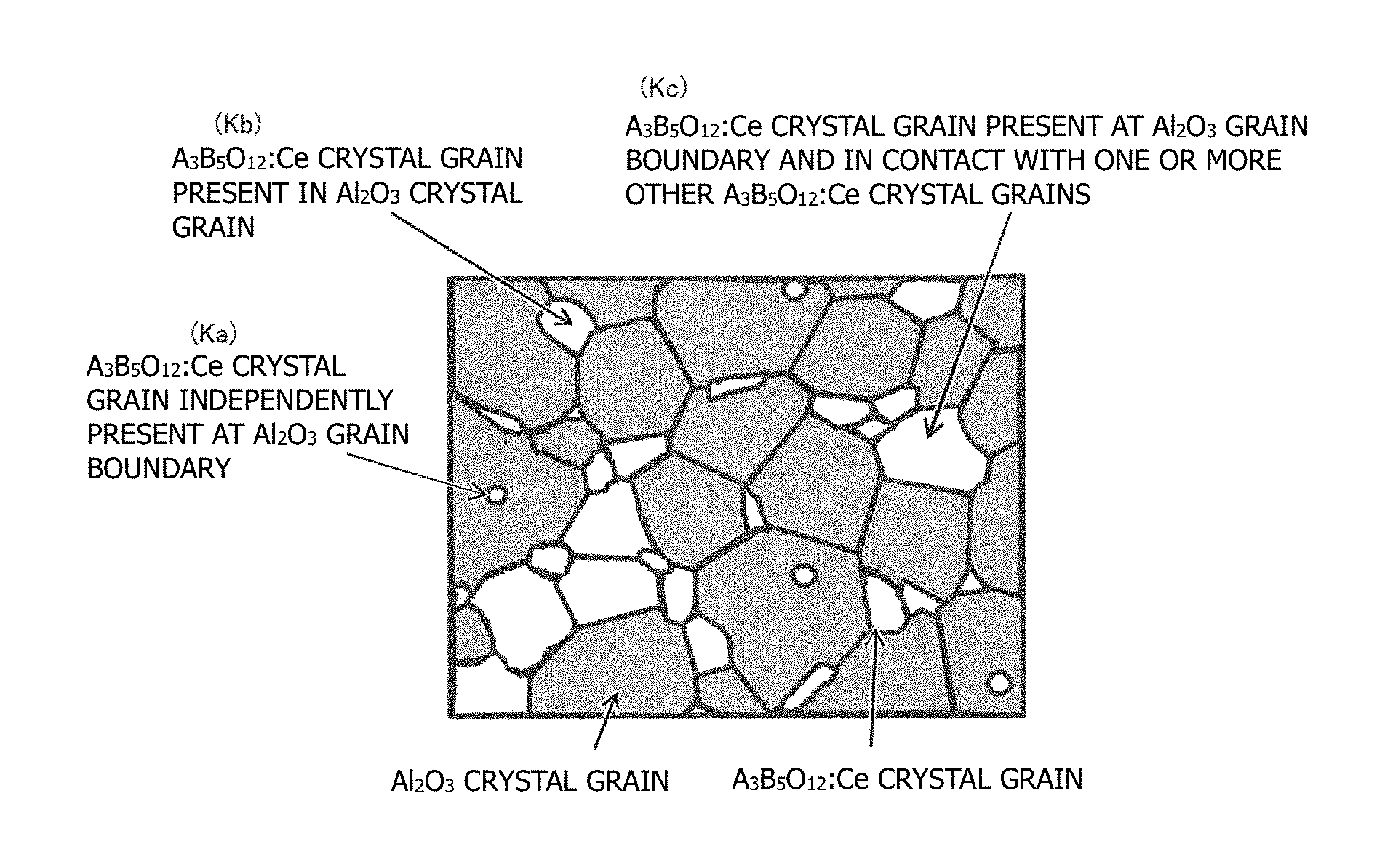
Problem to be Solved by the Invention
[0012] Since in the aforementioned prior techniques a garnet fluorescent component is deposited in Al.sub.2O.sub.3 without any particular control of the crystalline structure, the volume ratio of Al.sub.2O.sub.3/A.sub.3B.sub.5O.sub.12:Ce is used for preventing occurrence of color unevenness; i.e., for achieving high color uniformity. Thus, the resultant phosphor loses its important properties (e.g., fluorescence intensity and translucency) and thus fails to exhibit satisfactory fluorescent properties.
[0013] CeAl.sub.11O.sub.18, which is used in the technique disclosed in Patent Document 3, exhibits neither fluorescence nor translucency. Thus, incorporation of CeAl.sub.11O.sub.18 into a sintered body causes further loss of the aforementioned fluorescent properties.
[0014] In view of the foregoing, an object of the present invention is to provide an optical wavelength conversion member and a light-emitting device, each of which achieves compatibility between high fluorescence intensity and high color uniformity.
Means for Solving the Problem
[0015] (1) A first aspect of the present invention is directed to an optical wavelength conversion member comprising a polycrystalline ceramic sintered body containing, as main components, Al.sub.2O.sub.3 crystal grains and crystal grains of a component represented by formula A.sub.3B.sub.5O.sub.12:Ce.
[0016] In the optical wavelength conversion member, each of A and B of A.sub.3B.sub.5O.sub.12 is at least one element selected from the following element groups:
[0017] A: Sc, Y, and lanthanoids (except for Ce), and
[0018] B: Al and Ga; and
[0019] the following relations are satisfied:
[0020] 0%.ltoreq.X.ltoreq.25%,
[0021] 9%.ltoreq.Y.ltoreq.45%, and
[0022] 48%.ltoreq.Z.ltoreq.90%,
wherein X represents a proportion corresponding to the ratio a/N, Y represents a proportion corresponding to the ratio b/N, and Z represents a proportion corresponding to the ratio c/N, wherein N represents the total number of A.sub.3B.sub.5O.sub.12:Ce crystal grains present in a 20 .mu.m square region of a cross section of the ceramic sintered body; a represents the number of A.sub.3B.sub.5O.sub.12:Ce crystal grains present in Al.sub.2O.sub.3 crystal grains; b represents the number of A.sub.3B.sub.5O.sub.12:Ce crystal grains each being present at the Al.sub.2O.sub.3 crystal grain boundary and not in contact with another A.sub.3B.sub.5O.sub.12:Ce crystal grain; and c represents the number of A.sub.3B.sub.5O.sub.12:Ce crystal grains each being present at the Al.sub.2O.sub.3 crystal grain boundary and in contact with one or more other A.sub.3B.sub.5O.sub.12:Ce crystal grains.
[0023] Since the optical wavelength conversion member according to the first aspect has the aforementioned characteristic features, the optical wavelength conversion member achieves high fluorescence intensity and high color uniformity (i.e., low color unevenness) as shown in the Examples described hereinbelow. The optical wavelength conversion member will now be described in detail.
[0024] Since the A.sub.3B.sub.5O.sub.12:Ce crystal grains satisfying the condition X are completely incorporated into Al.sub.2O.sub.3 crystal grains, volatilization of Ce can be prevented. Thus, stable fluorescence with color uniformity is achieved without causing a variation in Ce content.
[0025] A proportion X more than 25% leads to a decrease in number of A.sub.3B.sub.5O.sub.12:Ce crystal grains each being independently present at an Al.sub.2O.sub.3 crystal grain boundary (corresponding to the proportion Y); hence, the effect of preventing growth of Al.sub.2O.sub.3 grains (so-called "pinning effect") is not exerted. Thus, Al.sub.2O.sub.3 grains are grown, and transmittance is lowered, resulting in low fluorescence intensity. A proportion X less than 1% tends to cause high color unevenness.
[0026] When the proportion Y falls within the aforementioned range, the pinning effect is exerted on Al.sub.2O.sub.3, and growth of Al.sub.2O.sub.3 grains is prevented. Consequently, translucency sufficient for extraction of fluorescence is achieved.
[0027] When the proportion Y is less than 9%, the pinning effect is not sufficiently exerted, and Al.sub.2O.sub.3 grains are grown, resulting in insufficient transmittance and thus low fluorescence intensity. In addition, coarsening of the grains is likely to cause color unevenness. When the proportion Y is more than 45%, optical dispersion increases at the Al.sub.2O.sub.3/A.sub.3B.sub.5O.sub.12:Ce grain boundary, and translucency is lowered, resulting in low fluorescence intensity.
[0028] When the proportion Z falls within the aforementioned range, translucency sufficient for extraction of fluorescence is achieved, since no optical dispersion occurs at the aforementioned A.sub.3B.sub.5O.sub.12:Ce/A.sub.3B.sub.5O.sub.12:Ce grain boundary.
[0029] When the proportion Z is less than 48%, fluorescence intensity is lowered due to insufficient translucency, whereas when the proportion Z is more than 90%, the amount of transmission of excitation light increases due to excessively high translucency, resulting in occurrence of color unevenness. In addition, the connection path between Al.sub.2O.sub.3 crystal grains is less likely to be formed, and thus thermal conductivity is lowered.
[0030] Therefore, when the proportions X, Y, and Z fall within the aforementioned ranges, high fluorescence intensity and high color uniformity can be achieved.
[0031] The optical wavelength conversion member according to the first aspect, which has the aforementioned characteristic features, exhibits high thermal conductivity. Thus, even when a high-output light source is used, an undesired effect of heat on the optical wavelength conversion member can be prevented; for example, optical loss can be prevented.
[0032] Since the optical wavelength conversion member is formed of a ceramic sintered body, the optical wavelength conversion member is advantageous in that it exhibits high strength, is less likely to undergo performance degradation through repeated irradiation with light from a light source, and exhibits excellent weatherability.
[0033] (2) In a second aspect of the present invention, the ceramic sintered body contains A.sub.3B.sub.5O.sub.12:Ce crystal grains in an amount of 5 to 50 vol. %.
[0034] Since the amount of A.sub.3B.sub.5O.sub.12:Ce crystal grains is 5 to 50 vol. % in the second aspect, the optical wavelength conversion member is advantageous in that it exhibits sufficient fluorescence intensity as shown in the Examples described hereinbelow.
[0035] (3) In a third aspect of the present invention, the amount of Ce is 10.0 mol % or less (exclusive of 0) relative to A in A.sub.3B.sub.5O.sub.12.
[0036] Since the amount of Ce is 10.0 mol % or less (exclusive of 0) relative to A in A.sub.3B.sub.5O.sub.12 in the third aspect, the optical wavelength conversion member is advantageous in that it exhibits sufficient fluorescence intensity as shown in the examples described hereinbelow.
[0037] (4) In a fourth aspect of the present invention, the Al.sub.2O.sub.3 crystal grains have a mean grain size of 0.3 to 10 .mu.m, and the A.sub.3B.sub.5O.sub.12:Ce crystal grains have a mean grain size of 0.3 to 5 .mu.m.
[0038] Since the Al.sub.2O.sub.3 crystal grains have a mean grain size of 0.3 to 10 .mu.m, and the A.sub.3B.sub.5O.sub.12:Ce crystal grains have a mean grain size of 0.3 to 5 .mu.m in the fourth aspect, the optical wavelength conversion member is advantageous in that it exhibits sufficient fluorescence intensity and appropriate translucency as shown in the Examples described hereinbelow.
[0039] The crystal grains having the aforementioned mean grain sizes readily achieve the aforementioned crystal grain conditions; i.e., proportions X, Y, and Z defined in the first aspect.
[0040] A fifth aspect of the invention is directed to a light-emitting device having an optical wavelength conversion member as recited in any one of claims 1 to 4.
[0041] The light (i.e., fluorescence) having a wavelength converted by means of the light-emitting device (specifically, the optical wavelength conversion member) according to the fifth aspect exhibits high fluorescence intensity and high color uniformity.
[0042] The light-emitting device may include any known light-emitting element, such as LED or LD.
<Characteristic Features of the Present Invention Will Now be Described>
[0043] The aforementioned "optical wavelength conversion member" is formed of a ceramic sintered body having the aforementioned characteristics. The grain boundary between crystal grains may contain, for example, some of the components forming the crystal grains or an unavoidable impurity.
[0044] The term "main components" described above refers to any component whose crystal grains are present in a predominant amount (volume) in the optical wavelength conversion member.
[0045] The term "A.sub.3B.sub.5O.sub.12:Ce" described above refers to the case where a portion of A contained in A.sub.3B.sub.5O.sub.12 is substituted by Ce through formation of a solid solution. The compound having such a structure exhibits fluorescent properties.
[0046] The term "cross section of the optical wavelength conversion member" described above refers to at least one cross section of a light-transmitting portion. In the case where a plurality of (e.g., five) cross sections are observed, the cross section in which the average values satisfy the aforementioned proportions X, Y, and Z can be used. When the proportions X, Y, and Z are determined at a plurality of (e.g., five) sites in each cross section, the average values can be used.
[0047] In order to achieve the proportions X, Y, and Z falling within the aforementioned ranges, the amount of a dispersant must be appropriately determined, or a firing process must be performed under appropriate conditions as described below. For example, an excessively low firing temperature leads to a decrease in proportion X, which is not preferred. An excessively large amount of a dispersant leads to a decrease in proportion Y, whereas an excessively small amount of a dispersant leads to an increase in proportion Z. Thus, the amount of a dispersant must be appropriately determined.
BRIEF DESCRIPTION OF THE DRAWINGS
[0048] FIG. 1 Schematic view showing the crystalline structure of an optical wavelength conversion member according to an embodiment.
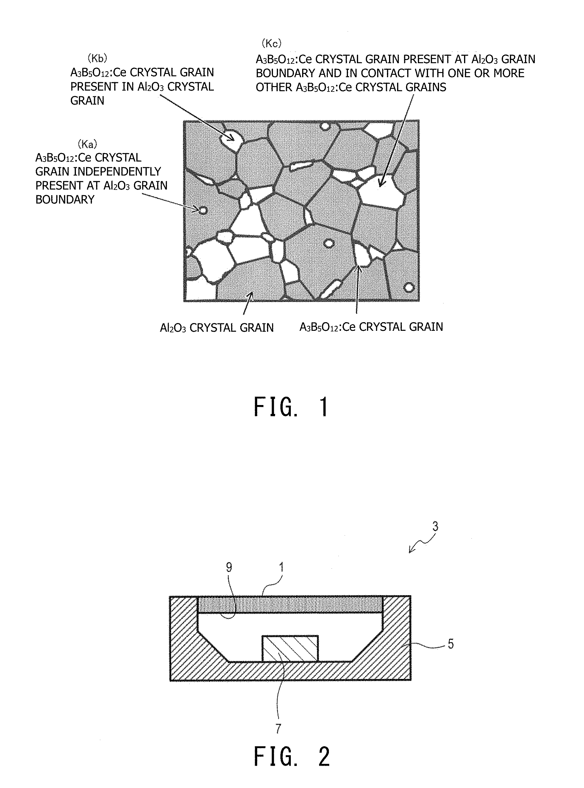
[0049] FIG. 2 Cross-sectional view of a light-emitting device in a thickness direction.
MODES FOR CARRYING OUT THE INVENTION
[0050] Next will be described an embodiment of the optical wavelength conversion member and the light-emitting device of the present invention.
1. EMBODIMENT
[1-1. Structure of Optical Wavelength Conversion Member]
[0051] An optical wavelength conversion member of the embodiment will now be described. As illustrated in FIG. 1, the optical wavelength conversion member 1 (see FIG. 2) of the embodiment is formed of, for example, a plate-like ceramic sintered body formed of a polycrystalline body containing, as main components, Al.sub.2O.sub.3 crystal grains and crystal grains of a component represented by formula A.sub.3B.sub.5O.sub.12:Ce (hereinafter may be referred to as "A.sub.3B.sub.5O.sub.12:Ce crystal grains").
[0052] In the optical wavelength conversion member 1, each of A and B of the A.sub.3B.sub.5O.sub.12 is at least one element selected from the following element groups:
[0053] A: Sc, Y, and lanthanoids (except for Ce), and
[0054] B: Al and Ga.
[0055] In addition, the following relations are satisfied:
[0056] 0%.ltoreq.X.ltoreq.25%,
[0057] 9%.ltoreq.Y.ltoreq.45%, and
[0058] 48%.ltoreq.Z.ltoreq.90%,
wherein X represents a proportion corresponding to the ratio a/N, Y represents a proportion corresponding to the ratio b/N, and Z represents a proportion corresponding to the ratio c/N, wherein N represents the total number of A.sub.3B.sub.5O.sub.12:Ce crystal grains present in a 20 .mu.m square region of a cross section of the ceramic sintered body; a represents the number of A.sub.3B.sub.5O.sub.12:Ce crystal grains present in Al.sub.2O.sub.3 crystal grains; b represents the number of A.sub.3B.sub.5O.sub.12:Ce crystal grains each being present at an Al.sub.2O.sub.3 crystal grain boundary and not in contact with another A.sub.3B.sub.5O.sub.12:Ce crystal grain; and c represents the number of A.sub.3B.sub.5O.sub.12:Ce crystal grains each being present at an Al.sub.2O.sub.3 crystal grain boundary and in contact with one or more other A.sub.3B.sub.5O.sub.12:Ce crystal grains.
[0059] In FIG. 1, Ka represents A.sub.3B.sub.5O.sub.12:Ce crystal grains corresponding to a (thus X); i.e., A.sub.3B.sub.5O.sub.12:Ce crystal grains present in Al.sub.2O.sub.3 crystal grains; Kb represents A.sub.3B.sub.5O.sub.12:Ce crystal grains corresponding to b (thus Y); i.e., A.sub.3B.sub.5O.sub.12:Ce crystal grains each being independently present at an Al.sub.2O.sub.3 crystal grain boundary; and Kc represents A.sub.3B.sub.5O.sub.12:Ce crystal grains corresponding to c (thus Z); i.e., A.sub.3B.sub.5O.sub.12:Ce crystal grains each being present at an Al.sub.2O.sub.3 crystal grain boundary and in contact with one or more other A.sub.3B.sub.5O.sub.12:Ce crystal grains.
[0060] In the present embodiment, the ceramic sintered body may contain A.sub.3B.sub.5O.sub.12:Ce crystal grains in an amount of 5 to 50 vol. %.
[0061] In the present embodiment, the amount of Ce may be 10.0 mol % or less (exclusive of 0) relative to A in A.sub.3B.sub.5O.sub.12.
[0062] In the present embodiment, Al.sub.2O.sub.3 crystal grains may have a mean grain size of 0.3 to 10 .mu.m, and A.sub.3B.sub.5O.sub.12:Ce crystal grains may have a mean grain size of 0.3 to 5 .mu.m.
[1-2. Structure of Light-Emitting Device]
[0063] As illustrated in FIG. 2, a light-emitting device 3 includes a box-shaped ceramic package (container) 5 formed of, for example, alumina; a light-emitting element 7 (e.g., an LD) disposed in the interior of the container 5; and the plate-like optical wavelength conversion member 1 disposed so as to cover an opening 9 of the container 5.
[0064] In the light-emitting device 3, light emitted from the light-emitting element 7 transmits through the optical wavelength conversion member 1, and the wavelength of a portion of the emitted light is converted in the interior of the optical wavelength conversion member 1. Thus, the optical wavelength conversion member 1 emits fluorescence having a wavelength different from that of light emitted from the light-emitting element 7.
[1-3. Effects]
[0065] The effects of the embodiment will now be described.
[0066] In the optical wavelength conversion member 1 of the present embodiment, since, for example, the proportions X, Y, and Z are specified as described above, high fluorescence intensity and high color uniformity can be achieved.
[0067] The optical wavelength conversion member 1 of the present embodiment exhibits high thermal conductivity. Thus, even when a high-output light source is used, an undesired effect of heat on the optical wavelength conversion member 1 can be prevented; for example, optical loss can be prevented.
[0068] Since the optical wavelength conversion member 1 of the present embodiment is formed of a ceramic sintered body, the optical wavelength conversion member 1 is advantageous in that it exhibits high strength, is less likely to undergo performance degradation through repeated irradiation with light from a light source, and exhibits excellent weatherability.
[0069] In the case where the amount of A.sub.3B.sub.5O.sub.12:Ce crystal grains is 5 to 50 vol. %, the optical wavelength conversion member 1 is advantageous in that it exhibits sufficient fluorescence intensity.
[0070] In the case where the amount of Ce is 10.0 mol % or less (exclusive of 0) relative to A in A.sub.3B.sub.5O.sub.12, the optical wavelength conversion member 1 is advantageous in that it exhibits sufficient fluorescence intensity.
[0071] In the case where Al.sub.2O.sub.3 crystal grains have a mean grain size of 0.3 to 10 .mu.m, and A.sub.3B.sub.5O.sub.12:Ce crystal grains have a mean grain size of 0.3 to 5 .mu.m, the optical wavelength conversion member 1 is advantageous in that it exhibits sufficient fluorescence intensity and appropriate translucency.
[0072] Thus, the light-emitting device 3 including the optical wavelength conversion member 1 can effectively emit fluorescence with high fluorescence intensity and high color uniformity.
2. EXAMPLES
[0073] Specific examples will next be described.
Example 1
[0074] Ceramic sintered body samples (Nos. 1 to 9) were prepared under the conditions shown in Tables 1 and 2. Samples Nos. 1 to 9 fall within the scope of the present invention.
[0075] Specifically, for preparation of each sample, Al.sub.2O.sub.3 powder (mean particle size: 0.3 .mu.m), Y.sub.2O.sub.3 powder (mean particle size: 1.2 .mu.m), and CeO.sub.2 powder (mean particle size: 1.5 .mu.m) were weighed so that the amount of YAG (Y.sub.3Al.sub.5O.sub.12) was 21 vol. % in a ceramic sintered body (i.e., a ceramic sintered body forming an optical wavelength conversion member), and the Ce content was 1 mol % relative to Y in YAG.
[0076] These powders were added to a ball mill together with pure water and a specific amount of a dispersant (2 wt. % in terms of solid content, relative to the raw material powders), and these materials were grind-mixed for 12 hours. The resultant slurry was dried and granulated, and the resultant granular product was formed into a compact. The compact was fired in air at ambient pressure and at 1,450.degree. C. to 1,750.degree. C. for 3 to 20 hours. Thus, ceramic sintered body samples Nos. 1 to 9 (e.g., plate-like samples) were prepared.
[0077] Examples of the usable dispersant include polycarboxylate dispersants, such as SN Dispersant 5468 (product of San Nopco Limited) and MALIALIM AKM-0531 (product of NOF Corporation).
[0078] Subsequently, the prepared ceramic sintered bodies were examined in terms of the following properties (a) to (f) in the same manner as in other examples described below. The results are shown in Table 2.
[0079] (a) Relative Density
[0080] The relative density of each ceramic sintered body was measured by the Archimedes method, and the measured density was converted into a relative density.
[0081] (b) Mean Crystal Grain Size
[0082] Each sample was subjected to mirror polishing and subsequent thermal etching at 1,300.degree. C. The etched surface was observed under a scanning electron microscope (i.e., SEM observation), to thereby prepare an image (magnification: 5,000) at a certain position of the ceramic sintered body. In the case where the sample is in the shape of, for example, rectangular plate, the position corresponds to a light-transmitting portion; i.e., a center portion (in plan view) as viewed in a thickness direction.
[0083] A line was drawn in a 20 .mu.m square region of the image at the aforementioned position (see, for example, FIG. 1), and the intercept method was used to determine the mean crystal grain sizes of Al.sub.2O.sub.3 crystal grains and that of A.sub.3B.sub.5O.sub.12:Ce crystal grains.
[0084] (c) Grain Proportions X, Y, and Z
[0085] In the same manner as in (b) described above, the sample was subjected to mirror polishing and subsequent thermal etching at 1,300.degree. C. The etched surface was subjected to SEM observation, to thereby prepare an image (magnification: 5,000) at a certain position of the ceramic sintered body. The number of grains (a, b, or c) was counted in a 20 .mu.m square region of the image, to thereby calculate a proportion X, Y, or Z. The aforementioned treatment was performed in five visual fields, and the proportions X, Y, or Z were averaged. The polished surface corresponds to the "cross section" as used herein.
[0086] (d) Fluorescence Intensity
[0087] Each sample was processed into a shape of 13 mm.times.13 mm.times.0.5 mm (thickness). Blue LD light (wavelength: 465 nm) was focused to a width of 0.5 mm by means of a lens, and the processed sample was irradiated with the focused light. The light transmitting through the sample was focused by means of a lens, and the emission intensity was measured by means of a power sensor. The sample was irradiated with the light at a power density 40 W/mm.sup.2. The emission intensity was evaluated by a value relative to that (taken as 100) of a YAG:Ce single-crystal body.
[0088] (e) Color Unevenness
[0089] Color unevenness (i.e., variation in color) was evaluated through determination of a variation in chromaticity by means of an illuminometer. Each sample was processed into a shape of 20 mm.times.20 mm.times.0.5 mm (thickness). Blue LD light (wavelength: 465 nm) was focused to a width of 0.5 mm by means of a lens, and the processed sample was irradiated with the focused light. A color illuminometer was used to determine the chromaticity of the light transmitting through the surface of the sample opposite the surface irradiated with the focused light.
[0090] The light irradiation was performed on a 18 mm square region (at intervals of 3 mm in the region) at the center of the irradiation surface of the sample (sample surface), and a variation (.DELTA.X) in chromaticity (in X-direction) was evaluated. As used herein, the term "variation (.DELTA.X)" refers to the maximum deviation of chromaticity (in X-direction)
[0091] The term "chromaticity" as used herein refers to a chromaticity indicated by the CIE-XYZ color system established by the International Commission on Illumination (CIE) in 1931. Specifically, the chromaticity is indicated by the xy chromaticity diagram (so-called CIE chromaticity diagram) wherein three primary colors of light are digitized and represented in an xy coordinate space.
[0092] (f) Thermal Conductivity
[0093] Each sample was processed into a shape of 10 mm.times.10 mm.times.2 mm (thickness), and the thermal conductivity of the sample was measured. Specifically, thermal conductivity was measured according to JIS R1611.
[0094] The above-determined fluorescence intensity, color unevenness, and thermal conductivity of each sample can be evaluated on the basis of the following criteria. Samples of other examples can be evaluated in the same manner.
[0095] Criteria for evaluation of fluorescence intensity are as follows: 110 or more (preferred), 100 or more and less than 110 (somewhat preferred), and less than 100 (not preferred). Criteria for evaluation of color unevenness are as follows: .DELTA.X<0.02 (preferred), 0.02.ltoreq..DELTA.X<0.06 (somewhat preferred), and 0.06.ltoreq..DELTA.X (not preferred).
[0096] Criteria for evaluation of thermal conductivity are as follows: 20 W/mK or more (preferred), and less than 20 W/mK (not preferred).
[0097] The samples of Example 1 were evaluated on the basis of the aforementioned criteria. Next will be described the results.
[0098] All the samples of Example 1 exhibited a relative density of 99% or more; i.e., the samples were sufficiently densified. The mean crystal grain size of Al.sub.2O.sub.3 (abbreviated as "Al.sub.2O.sub.3 grain size" in Table 2) was found to fall within a range of 0.3 to 10 .mu.m, and the mean crystal grain size of A.sub.3B.sub.5O.sub.12:Ce (YAG:Ce) (abbreviated as "A.sub.3B.sub.5O.sub.12 grain size" in Table 2) was found to fall within a range of 0.3 to 5 .mu.m.
[0099] Samples Nos. 3 to 9, in which X, Y, and Z fall within the scope of the present invention, exhibited good results in terms of fluorescence intensity, color unevenness, and thermal conductivity. Samples Nos. 1 and 2, which fall within the scope of the present invention (note: the firing temperature is lower than that for the other samples), exhibited color unevenness higher than that of samples Nos. 3 to 9.
Example 2
[0100] As shown in Tables 1 and 2, ceramic sintered body samples (samples Nos. 10 to 15) were prepared and evaluated in the same manner as in Example 1.
[0101] However, the amount of a dispersant was changed to fall within a range of 1.8 to 5 wt. % during mixing of the raw materials. The firing time was changed within a range of 5 to 20 hours.
[0102] Samples Nos. 11 to 14 fall within the scope of the present invention, and samples Nos. 10 and 15 (Comparative Examples) fall outside the scope of the present invention.
[0103] All the samples exhibited a relative density of 99% or more; i.e., the samples were sufficiently densified. Except for the case of sample No. 10, the mean crystal grain size of Al.sub.2O.sub.3 was found to fall within a range of 0.3 to 10 .mu.m, and the mean crystal grain size of A.sub.3B.sub.5O.sub.12:Ce (YAG:Ce) was found to fall within a range of 0.3 to 5 .mu.m. As shown in Table 2, samples Nos. 11 to 14, in which X, Y, and Z fall within the scope of the present invention, exhibited good results in terms of fluorescence intensity, color unevenness, and thermal conductivity. In sample No. 10 (lower Y), the mean crystal grain size of Al.sub.2O.sub.3 was 11 .mu.m (slightly coarse), the fluorescence intensity was slightly low, and the color unevenness was high. In sample No. 15 (higher Y and lower Z), the fluorescence intensity was less than 100.
Example 3
[0104] As shown in Tables 1 and 2, ceramic sintered body samples (samples Nos. 16 to 20) were prepared and evaluated in the same manner as in Example 1.
[0105] The amount of a dispersant was changed to fall within a range of 0 to 1.5 wt. % during mixing of the raw materials.
[0106] Samples Nos. 16 to 19 fall within the scope of the present invention, and sample No. 20 (Comparative Example) falls outside the scope of the present invention.
[0107] All the samples exhibited a relative density of 99% or more; i.e., the samples were sufficiently densified. The mean crystal grain size of Al.sub.2O.sub.3 was found to fall within a range of 0.3 to 10 .mu.m, and the mean crystal grain size of A.sub.3B.sub.5O.sub.12:Ce (YAG:Ce) was found to fall within a range of 0.3 to 5 .mu.m.
[0108] As shown in Table 2, samples Nos. 16 to 19, in which X, Y, and Z fall within the scope of the present invention, exhibited good results in terms of fluorescence intensity, color unevenness, and thermal conductivity. In sample No. 20 (lower Y and higher Z), the fluorescence intensity was slightly low, the color unevenness was high, and the thermal conductivity was low.
Example 4
[0109] As shown in Tables 1 and 2, ceramic sintered body samples (samples Nos. 21 to 28 falling within the scope of the present invention) were prepared and evaluated in the same manner as in Example 1.
[0110] The proportions of the raw materials were changed so that the amount of A.sub.3B.sub.5O.sub.12:Ce (amount of YAG:Ce) in the ceramic sintered body was adjusted to 1 to 60 vol. %.
[0111] All the samples exhibited a relative density of 99% or more; i.e., the samples were sufficiently densified. The mean crystal grain size of Al.sub.2O.sub.3 was found to fall within a range of 0.3 to 10 .mu.m, and the mean crystal grain size of A.sub.3B.sub.5O.sub.12:Ce (YAG:Ce) was found to fall within a range of 0.3 to 5 .mu.m.
[0112] As shown in Table 2, samples Nos. 23 to 27, in which the YAG:Ce content falls within a specific range (i.e., 5 to 50 vol. %), exhibited good results in terms of fluorescence intensity, color unevenness, and thermal conductivity. In samples Nos. 21 and 22 (lower YAG:Ce content), the fluorescence intensity was slightly low, and the color unevenness was slightly high. In sample No. 28 (higher YAG:Ce content), the fluorescence intensity was slightly low, and the thermal conductivity was low.
Example 5
[0113] As shown in Tables 1 and 2, ceramic sintered body samples (samples Nos. 29 to 38 falling within the scope of the present invention) were prepared and evaluated in the same manner as in Example 1.
[0114] The proportions of the raw materials were varied so that the Ce content was 0 to 15 mol % relative to Y in A.sub.3B.sub.5O.sub.12 (YAG) of the sintered body.
[0115] All the samples exhibited a relative density of 99% or more; i.e., the samples were sufficiently densified. The mean crystal grain size of Al.sub.2O.sub.3 was found to fall within a range of 0.3 to 10 .mu.m, and the mean crystal grain size of A.sub.3B.sub.5O.sub.12:Ce (YAG:Ce) was found to fall within a range of 0.3 to 5 .mu.m.
[0116] As shown in Table 2, samples Nos. 30 to 37, in which the Ce content falls within a specific range (i.e., 10.0 mol % or less (exclusive of 0)), exhibited good results in terms of fluorescence intensity, color unevenness, and thermal conductivity. In sample No. 29 (free of Ce), neither the fluorescence intensity nor the color unevenness was determined. In sample No. 38 (higher Ce content), the fluorescence intensity was slightly low.
Example 6
[0117] As shown in Tables 1 and 2, ceramic sintered body samples (samples Nos. 39 to 59 falling within the scope of the present invention) were prepared and evaluated in the same manner as in Example 1.
[0118] Y.sub.2O.sub.3 powder was used in combination with at least one of Lu.sub.2O.sub.3 powder (mean particle size: 1.3 .mu.m), Yb.sub.2O.sub.3 powder (mean particle size: 1.5 .mu.m), Gd.sub.2O.sub.3 powder (mean particle size: 1.5 .mu.m), Tb.sub.2O.sub.3 powder (mean particle size: 1.6 .mu.m), and Ga.sub.2O.sub.3 powder (mean particle size: 1.3 .mu.m). During mixing of the raw materials, the proportions of the raw materials were varied so that specific A.sub.3B.sub.5O.sub.12:Ce was synthesized.
[0119] All the samples exhibited a relative density of 99% or more; i.e., the samples were sufficiently densified. The mean crystal grain size of Al.sub.2O.sub.3 was found to fall within a range of 0.3 to 10 .mu.m, and the mean crystal grain size of A.sub.3B.sub.5O.sub.12:Ce (YAG:Ce) was found to fall within a range of 0.3 to 5 .mu.m.
[0120] All the ceramic sintered bodies exhibited good results in terms of fluorescence intensity, color unevenness, and thermal conductivity.
TABLE-US-00001 TABLE 1 Dispersant Firing Firing A.sub.3B.sub.5O.sub.12 content temperature time Example No. composition (wt %) (.degree. C.) (hr) 1 1 Y.sub.3Al.sub.5O.sub.12 2 1450 10 2 Y.sub.3Al.sub.5O.sub.12 2 1500 10 3 Y.sub.3Al.sub.5O.sub.12 2 1550 3 4 Y.sub.3Al.sub.5O.sub.12 2 1550 10 5 Y.sub.3Al.sub.5O.sub.12 2 1550 20 6 Y.sub.3Al.sub.5O.sub.12 2 1600 10 7 Y.sub.3Al.sub.5O.sub.12 2 1650 10 8 Y.sub.3Al.sub.5O.sub.12 2 1700 10 9 Y.sub.3Al.sub.5O.sub.12 2 1750 10 2 10 Y.sub.3Al.sub.5O.sub.12 5 1600 20 11 Y.sub.3Al.sub.5O.sub.12 4.5 1600 20 12 Y.sub.3Al.sub.5O.sub.12 4 1600 10 13 Y.sub.3Al.sub.5O.sub.12 3.5 1600 5 14 Y.sub.3Al.sub.5O.sub.12 3 1600 5 15 Y.sub.3Al.sub.5O.sub.12 1.8 1600 5 3 16 Y.sub.3Al.sub.5O.sub.12 1.5 1600 10 17 Y.sub.3Al.sub.5O.sub.12 1.2 1600 10 18 Y.sub.3Al.sub.5O.sub.12 0.8 1600 10 19 Y.sub.3Al.sub.5O.sub.12 0.3 1600 10 20 Y.sub.3Al.sub.5O.sub.12 0 1600 10 4 21 Y.sub.3Al.sub.5O.sub.12 2 1600 20 22 Y.sub.3Al.sub.5O.sub.12 2 1600 20 23 Y.sub.3Al.sub.5O.sub.12 2 1600 20 24 Y.sub.3Al.sub.5O.sub.12 2 1600 20 25 Y.sub.3Al.sub.5O.sub.12 2 1600 20 26 Y.sub.3Al.sub.5O.sub.12 2 1600 20 27 Y.sub.3Al.sub.5O.sub.12 2 1600 20 28 Y.sub.3Al.sub.5O.sub.12 3 1600 20 5 29 Y.sub.3Al.sub.5O.sub.12 2 1600 20 30 Y.sub.3Al.sub.5O.sub.12 2 1600 20 31 Y.sub.3Al.sub.5O.sub.12 2 1600 20 32 Y.sub.3Al.sub.5O.sub.12 2 1600 20 33 Y.sub.3Al.sub.5O.sub.12 2 1600 20 34 Y.sub.3Al.sub.5O.sub.12 2 1600 20 35 Y.sub.3Al.sub.5O.sub.12 2 1600 20 36 Y.sub.3Al.sub.5O.sub.12 2 1600 20 37 Y.sub.3Al.sub.5O.sub.12 2 1600 20 38 Y.sub.3Al.sub.5O.sub.12 2 1600 20 6 39 Lu.sub.3Al.sub.5O.sub.12 2 1600 20 40 Lu.sub.3Al.sub.5O.sub.12 2 1600 20 41 Lu.sub.3Al.sub.5O.sub.12 2 1600 20 42 Y.sub.1.5Lu.sub.1.5Al.sub.5O.sub.12 2 1600 20 43 Y.sub.1.5Lu.sub.1.5Al.sub.5O.sub.12 2 1600 20 44 Y.sub.1.5Lu.sub.1.5Al.sub.5O.sub.12 2 1600 20 45 Yb.sub.3Al.sub.5O.sub.12 2 1600 20 46 Yb.sub.3Al.sub.5O.sub.12 2 1600 20 47 Yb.sub.3Al.sub.5O.sub.12 2 1600 20 48 Y.sub.1.5Yb.sub.1.5Al.sub.5O.sub.12 2 1600 20 49 Y.sub.1.5Yb.sub.1.5Al.sub.5O.sub.12 2 1600 20 50 Y.sub.1.5Yb.sub.1.5Al.sub.5O.sub.12 2 1600 20 51 Y.sub.1.5Gd.sub.1.5Al.sub.5O.sub.12 2 1600 20 52 Y.sub.1.5Gd.sub.1.5Al.sub.5O.sub.12 2 1600 20 53 Y.sub.1.5Gd.sub.1.5Al.sub.5O.sub.12 2 1600 20 54 Y.sub.1.5Tb.sub.1.5Al.sub.5O.sub.12 2 1600 20 55 Y.sub.1.5Tb.sub.1.5Al.sub.5O.sub.12 2 1600 20 56 Y.sub.1.5Tb.sub.1.5Al.sub.5O.sub.12 2 1600 20 57 Y.sub.3Al.sub.4Ga.sub.1O.sub.12 2 1600 20 58 Y.sub.3Al.sub.4Ga.sub.1O.sub.12 2 1600 20 59 Y.sub.3Al.sub.4Ga.sub.1O.sub.12 2 1600 20
TABLE-US-00002 TABLE 2 Al.sub.2O.sub.3 A.sub.3B.sub.5O.sub.12:Ce Ce Color Thermal X Y Z content content content Fluorescence unevenness conductivity Al.sub.2O.sub.3 grain A.sub.3B.sub.5O.sub.12 grain Example No. (%) (%) (%) (vol. %) (vol. %) (mol %) intensity (.DELTA.X) (W/mK) size size 1 1 0 14.3 85.7 79 21 1 115 0.05 21.5 0.8 0.4 2 0.2 15.1 84.7 79 21 1 114 0.032 24.6 0.9 0.4 3 1.1 14.2 84.7 79 21 1 120 0.018 24.9 1.2 0.5 4 3.5 18.7 77.8 79 21 1 121 0.015 25.1 1.5 0.5 5 4.9 20.1 75 79 21 1 117 0.014 25.3 1.6 0.7 6 9.3 23.3 67.4 79 21 1 114 0.013 25.9 1.7 0.8 7 14.6 25.6 59.8 79 21 1 112 0.013 26.9 2.1 1 8 17.5 27.8 54.7 79 21 1 111 0.012 27.5 3.2 1.4 9 20.5 30.3 49.2 79 21 1 110 0.011 28.2 5.1 1.9 2 10 11.5 8.8 79.7 79 21 1 108 0.032 25.3 11 3.5 11 8.0 10.5 81.5 79 21 1 114 0.019 24.9 6.5 2.8 12 3.2 21.0 75.8 79 21 1 119 0.015 26.1 3.1 1.5 13 2.5 33.5 64.0 79 21 1 113 0.013 26.3 2.5 1.2 14 2.1 42.1 55.8 79 21 1 111 0.012 27.8 1.8 0.8 15 1.8 46.5 47.5 79 21 1 95 0.013 28.2 1.5 0.7 3 16 8.9 39.9 51.2 79 21 1 111 0.01 27.3 1.9 0.8 17 7.8 27.2 65.0 79 21 1 118 0.014 26 2.3 1 18 7.3 12.4 80.3 79 21 1 113 0.013 24.7 3.1 1.3 19 2.3 9.1 88.6 79 21 1 110 0.018 21.6 4.1 1.7 20 1.8 4.7 93.5 79 21 1 105 0.031 18.5 5 2 4 21 26.3 68.0 5.7 99 1 1 90 0.08 28.6 10 0.3 22 17.8 28.1 54.1 97 3 1 103 0.021 27.4 7.5 3.1 23 15.1 27.3 57.7 95 5 1 110 0.018 26.7 5.5 2.2 24 9.3 25.1 65.6 90 10 1 113 0.015 25 3.6 1.9 25 7.6 20.1 72.3 75 25 1 116 0.013 24.5 1.6 0.8 26 2.2 16.4 81.4 70 30 1 119 0.012 24.1 1.5 0.7 27 1.5 13.5 85.0 50 50 1 113 0.011 22.1 1.7 0.8 28 1.2 11.6 87.2 40 60 1 107 0.01 19 2.1 0.9 5 29 2.8 20.1 77.1 79 21 0 -- -- 26.2 1.9 0.8 30 2.9 21 76.1 79 21 0.03 110 0.019 26 1.8 0.8 31 3.2 22 74.8 79 21 0.3 111 0.018 26.9 1.9 0.7 32 3 20.5 76.5 79 21 0.45 113 0.016 26.5 1.9 0.8 33 2.6 19.9 77.5 79 21 0.5 117 0.014 25.9 2 0.9 34 2.1 18.7 79.2 79 21 1 118 0.012 24.5 2.1 0.9 35 2.8 18 79.2 79 21 3 117 0.013 25.5 1.8 0.7 36 3.3 18.8 77.9 79 21 5 116 0.013 25.8 1.7 0.6 37 3.6 20.5 75.9 79 21 10 111 0.011 26.7 1.8 0.7 38 3.1 19.5 77.4 79 21 15 103 0.014 25 1.9 0.7 6 39 3.5 21 75.5 90 10 1 112 0.012 27.9 3.1 1.5 40 2.5 23.5 74 79 21 1 115 0.015 26.5 1.8 0.8 41 2.8 26.1 71.1 70 30 1 118 0.016 25.8 1.5 1.2 42 4 20.7 75.3 90 10 1 111 0.015 28.4 3.2 1.4 43 3.1 24 72.9 79 21 1 113 0.018 27.1 1.7 0.9 44 2.6 19.9 77.5 70 30 1 116 0.01 25.6 1.5 1.2 45 2.9 23.5 73.6 90 10 1 114 0.012 28 3.3 1.3 46 2.4 18.7 78.9 79 21 1 114 0.014 26.5 1.9 0.8 47 1.9 23.5 74.6 70 30 1 119 0.015 24.9 1.6 1.1 48 1.8 23.9 74.3 90 10 1 112 0.017 27.5 3.5 1.6 49 2.4 24.6 73 79 21 1 115 0.013 26 1.9 0.8 50 2.7 28 69.3 70 30 1 118 0.012 23.9 1.5 1.3 51 2 21.9 76.1 90 10 1 114 0.01 27 2.9 1.3 52 2.5 23.5 74 79 21 1 116 0.01 25.9 1.7 0.7 53 3.5 24.3 72.2 70 30 1 118 0.016 24.9 1.4 1.2 54 3.1 28.1 70.8 90 10 1 113 0.014 28.2 3 1.5 55 3 24 73 79 21 1 113 0.011 26.3 1.6 0.8 56 2.9 27 70.1 70 30 1 115 0.019 25.7 1.5 1.2 57 2.4 24.6 73 90 10 1 110 0.014 27.9 3.1 1.3 58 3.3 25.3 71.4 79 21 1 112 0.017 26 1.8 0.9 59 2.9 21 76.1 70 30 1 115 0.012 25.1 1.4 1.2
3. OTHER EMBODIMENTS
[0121] Needless to say, the present invention is not limited to the aforementioned embodiment, but may be implemented in various other forms without departing from the scope of the invention.
[0122] (1) For example, the aforementioned embodiment involves the use of a firing process performed in air at ambient pressure. However, a vacuum firing process, a reducing-atmosphere firing process, a hot pressing (HP) process, a hot isostatic pressing (HIP) process, or any combination of these processes may be used for the preparation of a sample having the same properties as those described in the embodiment.
[0123] (2) The aforementioned optical wavelength conversion member or light-emitting device can be used for various applications, including fluorescent bodies, optical wavelength conversion apparatuses, head lamps, lighting apparatuses, and optical apparatuses (e.g., projectors).
[0124] (3) In the aforementioned embodiment, the function of a single component may be shared by a plurality of components, or a single component may exert the functions of a plurality of components. Some of the components in the aforementioned embodiment may be omitted. At least some of the components in the aforementioned embodiment may be, for example, added to or replaced with components in another embodiment. Embodiments of the present invention encompass any form included in technical ideas specified by the appended claims.
DESCRIPTION OF REFERENCE NUMERALS
[0125] 1: optical wavelength conversion member; 3: light-emitting device; and 7: light-emitting element
* * * * *
D00000
D00001
XML
uspto.report is an independent third-party trademark research tool that is not affiliated, endorsed, or sponsored by the United States Patent and Trademark Office (USPTO) or any other governmental organization. The information provided by uspto.report is based on publicly available data at the time of writing and is intended for informational purposes only.
While we strive to provide accurate and up-to-date information, we do not guarantee the accuracy, completeness, reliability, or suitability of the information displayed on this site. The use of this site is at your own risk. Any reliance you place on such information is therefore strictly at your own risk.
All official trademark data, including owner information, should be verified by visiting the official USPTO website at www.uspto.gov. This site is not intended to replace professional legal advice and should not be used as a substitute for consulting with a legal professional who is knowledgeable about trademark law.