Display Panel, Manufacturing Method Therof, And Display Device
TIAN; Pengcheng ; et al.
U.S. patent application number 16/322273 was filed with the patent office on 2019-06-27 for display panel, manufacturing method therof, and display device. The applicant listed for this patent is BEIJING BOE OPTOELECTRONICS TECHNOLOGY CO., LTD., BOE TECHNOLOGY GROUP CO., LTD.. Invention is credited to Xin LI, Pengcheng TIAN, Le ZHANG, Bin ZHAO, Detao ZHAO.
| Application Number | 20190196237 16/322273 |
| Document ID | / |
| Family ID | 58848584 |
| Filed Date | 2019-06-27 |
| United States Patent Application | 20190196237 |
| Kind Code | A1 |
| TIAN; Pengcheng ; et al. | June 27, 2019 |
DISPLAY PANEL, MANUFACTURING METHOD THEROF, AND DISPLAY DEVICE
Abstract
The present disclosure provides a display panel, a manufacturing method thereof and a display device. The display panel includes an opposite substrate and a display substrate opposite each other, a sealant is disposed between the opposite substrate and the display substrate, and the display substrate may be divided into a display area and a peripheral area around the display area. The display substrate includes a first base substrate; a first resin pattern on the first base substrate in the display area; and a protection layer in the display area and the peripheral area and between the first resin pattern and the first base substrate. The sealant is in the peripheral area and in contact with a portion of the protection layer in the peripheral area.
| Inventors: | TIAN; Pengcheng; (Beijing, CN) ; ZHAO; Bin; (Beijing, CN) ; LI; Xin; (Beijing, CN) ; ZHAO; Detao; (Beijing, CN) ; ZHANG; Le; (Beijing, CN) | ||||||||||
| Applicant: |
|
||||||||||
|---|---|---|---|---|---|---|---|---|---|---|---|
| Family ID: | 58848584 | ||||||||||
| Appl. No.: | 16/322273 | ||||||||||
| Filed: | March 21, 2018 | ||||||||||
| PCT Filed: | March 21, 2018 | ||||||||||
| PCT NO: | PCT/CN2018/079737 | ||||||||||
| 371 Date: | January 31, 2019 |
| Current U.S. Class: | 1/1 |
| Current CPC Class: | G02F 2201/42 20130101; G02F 1/1339 20130101; G02F 1/136209 20130101; G02F 1/133345 20130101; G02F 1/13306 20130101 |
| International Class: | G02F 1/1339 20060101 G02F001/1339; G02F 1/1362 20060101 G02F001/1362; G02F 1/133 20060101 G02F001/133 |
Foreign Application Data
| Date | Code | Application Number |
|---|---|---|
| Mar 21, 2017 | CN | 201710169527.0 |
Claims
1-13. (canceled)
14. A display panel, comprising: an opposite substrate; a display substrate, the display substrate and the opposite substrate being opposite to each other with a sealant disposed therebetween, the display substrate comprising a display area and a peripheral area around the display area, wherein the display substrate comprises: a first base substrate; a first resin pattern on the first base substrate in the display area; and a protection layer in the display area and the peripheral area and between the first resin pattern and the first base substrate; wherein the sealant is in the peripheral area, and the sealant is in contact with at least a part of a portion of the protection layer in the peripheral area.
15. The display panel of claim 14, wherein the sealant is in contact with the entire portion of the protection layer in the peripheral area.
16. The display panel of claim 14, further comprising a second resin pattern on a part of the portion of the protection layer in the peripheral area, wherein the protection layer is also between the second resin pattern and the first base substrate; and the sealant is in contact with a remaining part, on which the second resin pattern is not provided, of the portion of the protection layer in the peripheral area.
17. The display panel of claim 16, wherein the first resin pattern and the second resin pattern are in a same layer.
18. The display panel of claim 14, wherein a material of the protection layer is silicon nitride.
19. The display panel of claim 14, wherein the display substrate further comprises a metal pattern between the protection layer and first base substrate.
20. The display panel of claim 14, further comprising a gate drive circuit, wherein: the gate drive circuit is in the peripheral area, the metal pattern and the gate drive circuit are in a same layer, and the protection layer is on the gate drive circuit.
21. The display panel of claim 19, wherein the display substrate further comprises a via hole penetrating through the first resin pattern and the protection layer to reach the metal pattern and exposing a part of the metal pattern.
22. The display panel of claim 14, wherein the display substrate is an array substrate, the opposite substrate is a color filter substrate, and liquid crystal is between the array substrate and the color filter substrate.
23. The display panel of claim 14, wherein the opposite substrate comprises: a second base substrate; and a black matrix and color filter blocks on a side of the second base substrate close to the first base substrate.
24. The display panel of claim 23, wherein a back electrode made of a transparent conductive material is on a side of the second base substrate distal to the first base substrate.
25. The display panel of claim 24, further comprising a first polarizer on a side of the first base substrate distal to the second base substrate and a second polarizer on a side of the back electrode distal to the second base substrate.
26. A display device, comprising the display panel of claim 14.
27. A method for manufacturing a display panel, comprising: preparing a display substrate, wherein the display substrate is divided into a display area and a peripheral area located around the display area, and the display substrate comprises: a first base substrate, a first resin pattern located on the first base substrate in the display area, and a protection layer located in both the display area and the peripheral area and formed between the first resin pattern and the first base substrate; preparing an opposite substrate; and arranging the display substrate and the opposite substrate to be opposite to each other and providing a sealant between the display substrate and the opposite substrate, wherein the sealant is located in the peripheral area, and the sealant is in contact with at least a part of a portion of the protection layer in the peripheral area.
28. The method of claim 27, wherein preparing the display substrate further comprises: forming a metal pattern between the protection layer and first base substrate, and forming a via hole penetrating through the first resin pattern and the protection layer to reach the metal pattern and exposing a part of the metal pattern.
29. The method of claim 28, wherein preparing the display substrate further comprises: forming a gate drive circuit on the first base substrate, wherein: the gate drive circuit is located in the peripheral area, and the metal pattern and the gate drive circuit are formed in a same layer; and the protection layer is formed on the gate drive circuit.
30. The method of claim 28, wherein forming the first resin pattern comprises: forming a resin material layer on the protection layer, exposing the resin material layer using a mask plate to form an exposure pattern, the exposure pattern comprising a resin removed region, a resin partly remaining region, and a resin completely remaining region, wherein the resin partly remaining region comprises a removable portion and a remaining portion; developing the exposure pattern to remove the resin removed region and the removable portion of the resin partly remaining region; etching a portion of the protection layer corresponding to the resin removed region to form the via hole; and removing the remaining portion of the resin partly remaining region to expose the portion of the protection layer in the peripheral area, and thinning the resin completely remaining region to form the first resin pattern, wherein the resin completely remaining region corresponds to the first resin pattern, and the resin partly remaining region corresponds to the portion of the protection layer in the peripheral area.
31. The method of claim 27, wherein the sealant is formed on the entire portion of the protection layer in the peripheral area.
32. The method of claim 30, wherein thinning the resin completely remaining region further comprises forming a second resin pattern, wherein the second resin pattern is located in a part of the peripheral area, the resin completely remaining region further corresponds to the second resin pattern, and the resin partly remaining region corresponds to a part, on which the second resin pattern is not formed, of the portion of the protection layer in the peripheral area.
33. The method of claim 32, wherein the sealant is formed on the part of the portion of the protection layer in the peripheral area and on the second resin pattern.
Description
CROSS-REFERENCE TO RELATED APPLICATIONS
[0001] This is a National Phase Application filed under 35 U.S.C. 371 as a national stage of PCT/CN2018/079737, filed on Mar. 21, 2018, an application claiming the priority of Chinese Patent Application No. 201710169527.0, filed on Mar. 21, 2017, the contents of which are incorporated herein in their entirety by reference.
TECHNICAL FIELD
[0002] The present disclosure relates to the field of display technology, and in particular, relates to a display panel, a manufacturing method thereof, and a display device.
BACKGROUND
[0003] With the development of display technology, liquid crystal display devices have been used more and more widely. A liquid crystal display device may include an array substrate and a color filter substrate opposite to each other. The array substrate may be divided into a display area and a peripheral area around the display area. A gate drive circuit (e.g., Gate On Array, GOA for short) and a metal wiring connected to the gate drive circuit are formed in the peripheral area, and a protection layer is provided on the gate drive circuit and the metal wiring.
SUMMARY
[0004] The present disclosure provides a display panel, a manufacturing method thereof, and a display device.
[0005] According to an aspect of the present disclosure, there is provided a display panel, including:
[0006] an opposite substrate;
[0007] a display substrate, the display substrate and the opposite substrate being opposite to each other with a sealant disposed therebetween, the display substrate including a display area and a peripheral area around the display area, wherein the display substrate includes: [0008] a first base substrate; [0009] a first resin pattern on the first base substrate in the display area; [0010] a protection layer in the display area and the peripheral area and between the first resin pattern and the first base substrate;
[0011] wherein the sealant is in the peripheral area, and the sealant is in contact with at least a part of a portion of the protection layer in the peripheral area.
[0012] According to an embodiment of the present disclosure, the sealant is in contact with the entire portion of the protection layer in the peripheral area.
[0013] According to an embodiment of the present disclosure, the display panel further includes a second resin pattern on a part of the portion of the protection layer in the peripheral area, and the protection layer is also between the second resin pattern and the first base substrate; and
[0014] the sealant is in contact with a remaining part, on which the second resin pattern is not provided, of the portion of the protection layer in the peripheral area.
[0015] According to an embodiment of the present disclosure, the first resin pattern and the second resin pattern are in a same layer.
[0016] According to an embodiment of the present disclosure, a material of the protection layer is silicon nitride.
[0017] According to an embodiment of the present disclosure, the display substrate further includes a metal pattern between the protection layer and first base substrate
[0018] According to an embodiment of the present disclosure, the display panel further includes a gate drive circuit, wherein:
[0019] the gate drive circuit is in the peripheral area,
[0020] the metal pattern and the gate drive circuit are in a same layer, and
[0021] the protection layer is on the gate drive circuit.
[0022] According to an embodiment of the present disclosure, the display substrate further includes a via hole penetrating through the first resin pattern and the protection layer to reach the metal pattern and exposing a part of the metal pattern.
[0023] According to an embodiment of the present disclosure, the display substrate is an array substrate, the opposite substrate is a color filter substrate, and liquid crystal is between the array substrate and the color filter substrate.
[0024] According to an embodiment of the present disclosure, the opposite substrate includes: a second base substrate; and a black matrix and color filter blocks on a side of the second base substrate close to the first base substrate.
[0025] According to an embodiment of the present disclosure, a back electrode made of a transparent conductive material is on a side of the second base substrate distal to the first base substrate.
[0026] According to an embodiment of the present disclosure, the display panel includes a first polarizer on a side of the first base substrate distal to the second base substrate and a second polarizer on a side of the back electrode distal to the second base substrate.
[0027] According to an embodiment of the present disclosure, the display panel further includes a via hole penetrating through the protection layer and the first resin pattern to reach the metal pattern and exposing a part of the metal pattern.
[0028] According to another aspect of the present disclosure, there is provided a display device including the above display panel.
[0029] According to another aspect of the present disclosure, there is provided a method for manufacturing a display panel, including:
[0030] preparing a display substrate, wherein the display substrate is divided into a display area and a peripheral area around the display area, and the display substrate includes: [0031] a first base substrate, [0032] a first resin pattern on the first base substrate in the display area, and [0033] a protection layer located in both the display area and the peripheral area and formed between the first resin pattern and the first base substrate;
[0034] preparing an opposite substrate; and
[0035] arranging the display substrate and the opposite substrate to be opposite to each other and providing a sealant between the display substrate and the opposite substrate, wherein the sealant is located in the peripheral area, and the sealant is in contact with at least a part of a portion of the protection layer in the peripheral area.
[0036] According to an embodiment of the present disclosure, preparing the display substrate further includes: forming a metal pattern between the protection layer and first base substrate, and forming a via hole penetrating through the first resin pattern and the protection layer to reach the metal pattern and exposing a part of the metal pattern.
[0037] According to an embodiment of the present disclosure, preparing the display substrate includes:
[0038] forming the protection layer on the first base substrate; and
[0039] forming the first resin pattern on the protection layer.
[0040] According to an embodiment of the present disclosure, preparing the display substrate further includes: forming a gate drive circuit on the first base substrate, wherein:
[0041] the gate drive circuit is located in the peripheral area,
[0042] the metal pattern and the gate drive circuit are formed in a same layer, and
[0043] the protection layer is formed on the gate drive circuit.
[0044] According to an embodiment of the present disclosure, forming the first resin pattern on the protection layer includes:
[0045] forming a resin material layer on the protection layer,
[0046] exposing the resin material layer using a mask plate to form an exposure pattern, the exposure pattern including a resin removed region, a resin partly remaining region, and a resin completely remaining region, wherein the resin partly remaining region includes a removable portion and a remaining portion;
[0047] developing the exposure pattern to remove the resin removed region and the removable portion of the resin partly remaining region;
[0048] etching a portion of the protection layer corresponding to the resin removed region to form the via hole; and
[0049] removing the remaining portion of the resin partly remaining region to expose the portion of the protection layer in the peripheral area, and thinning the resin completely remaining region to form the first resin pattern, wherein the resin completely remaining region corresponds to the first resin pattern, and the resin partly remaining region corresponds to the portion of the protection layer in the peripheral area.
[0050] According to an embodiment of the present disclosure, the sealant is formed on the entire portion of the protection layer in the peripheral area.
[0051] According to an embodiment of the present disclosure, thinning the resin completely remaining region further includes forming a second resin pattern, wherein the second resin pattern is located in a part of the peripheral area, the resin completely remaining region further corresponds to the second resin pattern, and the resin partly remaining region corresponds to a part, on which the second resin pattern is not formed, of the portion of the protection layer in the peripheral area.
[0052] According to an embodiment of the present disclosure, the sealant is formed on the part of the portion of the protection layer in the peripheral area and on the second resin pattern.
BRIEF DESCRIPTION OF THE DRAWINGS
[0053] FIG. 1 is a schematic structural diagram of a display panel according to an embodiment of the present disclosure;
[0054] FIG. 2 is a schematic structural diagram of a display panel according to an embodiment of the present disclosure;
[0055] FIG. 3 is a flowchart of a method for manufacturing a display panel according to an embodiment of the present disclosure;
[0056] FIG. 4a is a schematic diagram of forming a protection layer according to an embodiment of the present disclosure;
[0057] FIG. 4b is a schematic diagram of forming a resin material layer according to an embodiment of the present disclosure;
[0058] FIG. 4c is a schematic diagram of exposing a resin material layer according to an embodiment of the present disclosure;
[0059] FIG. 4d is a schematic diagram of developing an exposure pattern according to an embodiment of the present disclosure;
[0060] FIG. 4e is a schematic diagram of forming a via hole according to an embodiment of the present disclosure; and
[0061] FIG. 4f is a schematic diagram of forming a first resin pattern according to an embodiment of the present disclosure.
DETAILED DESCRIPTION
[0062] In order to enable those skilled in the art to better understand technical solutions of the present disclosure, a display panel, a manufacturing method thereof and a display device provided by the present disclosure will be described in detail below with reference to the accompanying drawings.
[0063] In a manufacturing process of an array substrate, it is necessary to etch a protection layer using a mask. For this purpose, a resin layer, as a mask, may be provided on the protection layer to fully cover the display area and the peripheral area. In a process of assembling the array substrate with a color filter substrate, a sealant needs to be provided in the peripheral area. Since the resin layer is provided in the peripheral area, the sealant can only contact with the resin layer, resulting in that the peeling off of the sealant from the array substrate is likely to occur.
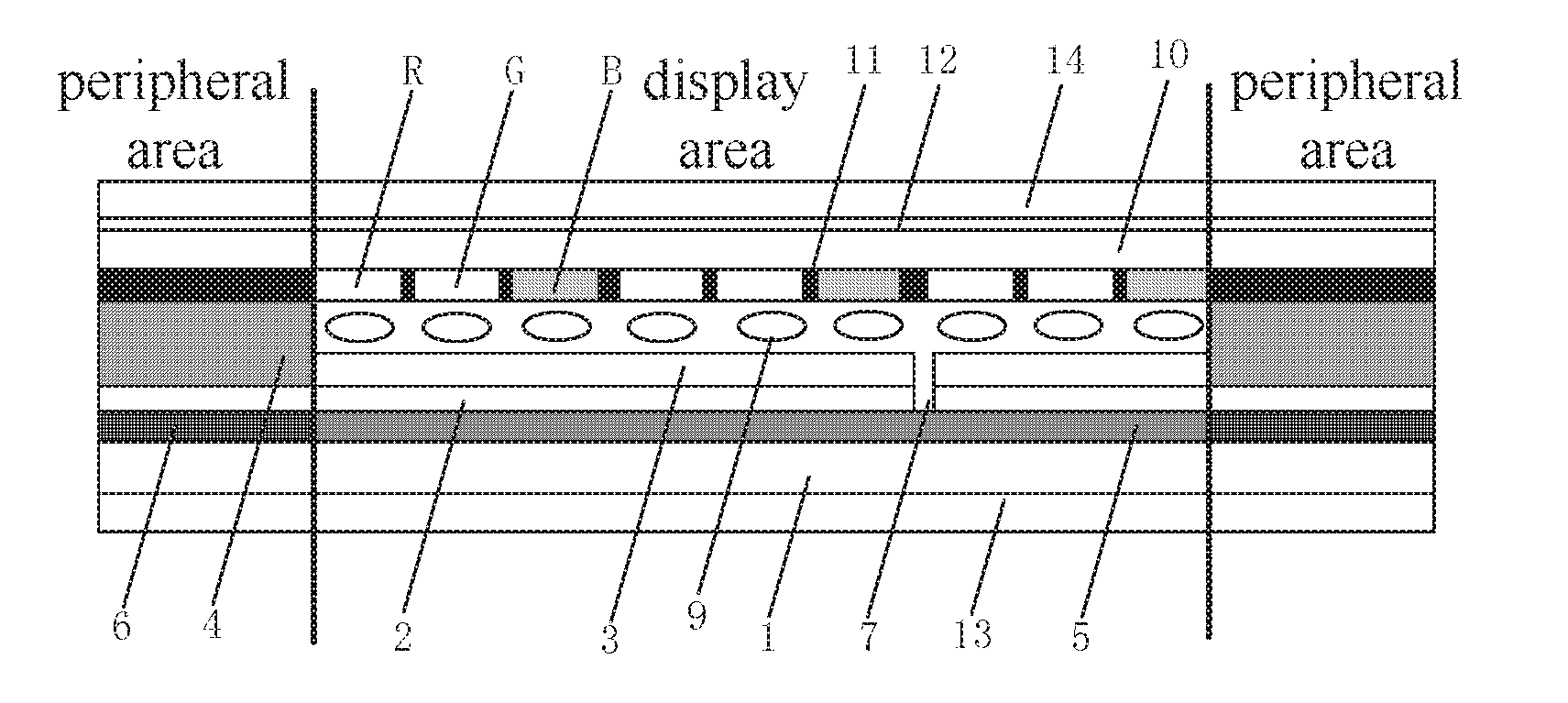
[0064] FIG. 1 is a schematic structural diagram of a display panel according to an embodiment of the present disclosure. As shown in FIG. 1, the display panel includes an opposite substrate and a display substrate opposite to each other, a sealant 4 is provided between the display substrate and the opposite substrate, and the display substrate may be divided into a display area and a peripheral area in the periphery of the display area. The display substrate may include a first base substrate 1, a first resin pattern 3 on the first base substrate 1 and in the display area, and a protection layer 2 in both the display area and the peripheral area and between the first resin pattern 3 and the first base substrate 1. The sealant 4 is located in the peripheral area, and the sealant 4 is in contact with a portion of the protection layer 2 in the peripheral area.
[0065] In an embodiment, the first resin pattern 3 is located on only a portion of the protection layer 2 in the display area, and is not provided in the peripheral area. No resin pattern is provided on the portion of the protection layer 2 in the peripheral area, so that the entire portion of the protection layer 2 in the peripheral area is exposed, and thus the sealant 4 is in contact with the entire portion of the protection layer 2 in the peripheral area.
[0066] In an embodiment, the display substrate further includes a metal pattern 5 and a gate drive circuit 6 on the first base substrate 1, and the protection layer 2 is located on the metal pattern 5 and the gate drive circuit 6. The metal pattern 5 is located in the display area, and the gate drive circuit 6 is located in the peripheral area. In an embodiment, the metal pattern 5 and the gate drive circuit 6 may be disposed in a same layer. In another embodiment, the display panel further includes a metal wiring (not shown) connected to the gate drive circuit 6, and the metal wiring is located in the peripheral area and between the first base substrate 1 and the protection layer 2.
[0067] In an embodiment, a via hole 7 penetrating through both the protection layer 2 and the first resin pattern 3 may be provided, and the via hole 7 reaches the metal pattern 5 and exposes a part of the metal pattern 5. In another embodiment, an electrode pattern (not shown) may be disposed on the first resin pattern 3, and a part of the electrode pattern is located in the via hole 7 and thus in contact with the exposed metal pattern 5, thereby realizing connection between the electrode pattern and the metal pattern 5. In the embodiment, the electrode pattern may be a pixel electrode, and the material of the pixel electrode may be indium tin oxide ITO.
[0068] In an embodiment, the material of the protection layer 2 may be silicon nitride SiNx. The bonding force between the sealant and the protection layer 2 made of such a material is relatively strong, so that the bonding force between the sealant and the display substrate can be enhanced.
[0069] In an embodiment, the display substrate is an array substrate, the opposite substrate is a color filter substrate, and liquid crystal 9 may be disposed between the display substrate and the opposite substrate.
[0070] In an embodiment, the opposite substrate may include: a second base substrate 10; and a black matrix 11 and color resist blocks both on a side of the second base substrate 10 close to the first base substrate 1. The black matrix 11 is located among the color resist blocks. In the embodiment, the color resist blocks may have a plurality of colors, for example, may include a red color resist block R, a green color resist block G and a blue color resist block B, which may be sequentially arranged.
[0071] In an embodiment, a back electrode 12 may be disposed on a side of the second base substrate 10 distal to the first base substrate 1, and the back electrode 12 may be made of a transparent conductive material (e.g., ITO).
[0072] In an embodiment, a first polarizer 13 may be disposed on a side of the first base substrate 1 distal to the second base substrate 10.
[0073] In an embodiment, a second polarizer 14 may be disposed on a side of the second base substrate 10 distal to the first base substrate 1. In the embodiment, the second polarizer 14 may be located on a side of the back electrode 12 distal to the second base substrate 10.
[0074] In the display panel according to the embodiments, the first resin pattern is located in the display area, and the sealant is in contact with the portion of the protection layer in the peripheral area, so that the case where the sealant is only in contact with the resin layer in the peripheral area is avoided and the bonding force between the sealant and the display substrate is enhanced, thereby greatly reducing the undesirable phenomenon of peeling off of the sealant from the display substrate.
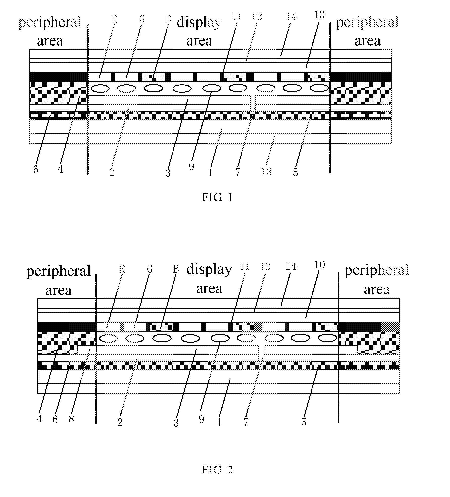
[0075] FIG. 2 is a schematic structural diagram of a display panel according to an embodiment of the present disclosure. As shown in FIG. 2, in the embodiment, the display substrate may further include a second resin pattern 8. The second resin pattern 8 is located on a part of the portion of the protection layer 2 in the peripheral area, and the protection layer 2 is located between the second resin pattern 8 and the first base substrate 1. The sealant 4 is in contact with the remaining part, on which the second resin pattern 8 is not disposed, of the portion of the protection layer 2 in the peripheral area.
[0076] In the embodiment, the second resin pattern 8 is disposed on a part of the portion of the protection layer 2 in the peripheral area, no resin pattern is disposed on the remaining part of the portion of the protection layer 2 in the peripheral area, the remaining part of the portion of the protection layer 2 is exposed, and therefore, the sealant 4 is in contact with the exposed remaining part of the portion of the protection layer 2 in the peripheral area.
[0077] In the embodiment, the second resin pattern 8 is located at a position, close to the display area, in the peripheral area, and is connected to the first resin pattern 3. In another embodiment, the second resin pattern 8 may also be located at other position in the peripheral area, which is not listed one by one herein.
[0078] In the embodiment, the first resin pattern 3 may be disposed in the same layer as the second resin pattern 8.
[0079] For the description of the other structures in the embodiment, reference may be made to the embodiments described with reference to FIG. 1, and details thereof are not repeatedly described herein.
[0080] In the display panel according to the embodiments, the first resin pattern is located in the display area, the second resin pattern is located at only a part of the peripheral area, and the sealant is in contact with a part, on which the second resin pattern is not disposed, of the portion of the protection layer in the peripheral area, so that the case where the sealant is only in contact with the resin layer in the peripheral area is avoided and the bonding force between the sealant and the display substrate is enhanced, thereby greatly reducing the undesirable phenomenon of peeling off of the sealant from the display substrate.
[0081] Another embodiment of the present disclosure provides a display device including a display panel.
[0082] The display panel in the embodiment may be a display panel provided in the embodiment described with reference to FIG. 1 or FIG. 2. Detailed description thereof may refer to the foregoing embodiments, and is not repeatedly given herein.
[0083] In the display device provided in the embodiment, the first resin pattern is located in the display area, and the sealant is in contact with the portion of the protection layer in the peripheral area, so that the case where the sealant is only in contact with the resin layer in the peripheral area is avoided and the bonding force between the sealant and the display substrate is enhanced, thereby greatly reducing the undesirable phenomenon of peeling off of the sealant from the display substrate.
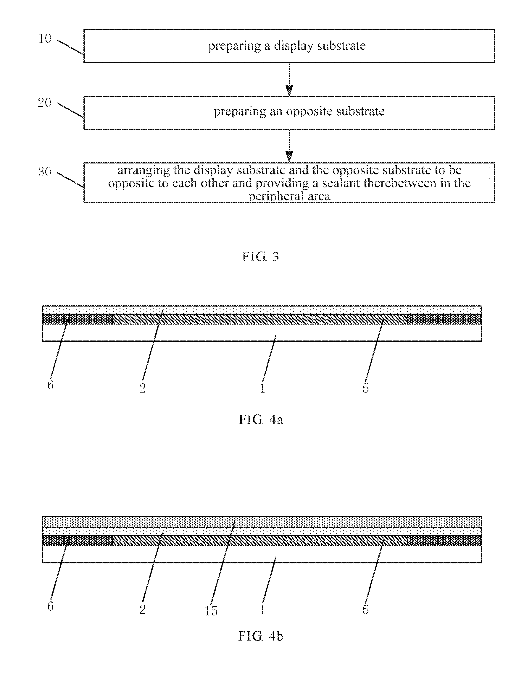
[0084] FIG. 3 is a flowchart of a method for manufacturing a display panel according to an embodiment of the present disclosure. As shown in FIG. 3, the method includes the steps as follows.
[0085] At step 10, a display substrate is prepared. The display substrate may be divided into a display area and a peripheral area located around the display area, and the display substrate includes a first base substrate, a protection layer, and a first resin pattern. The protection layer is located in both the display area and the peripheral area and formed between the first resin pattern and the first base substrate, and the first resin pattern is located in the display area.
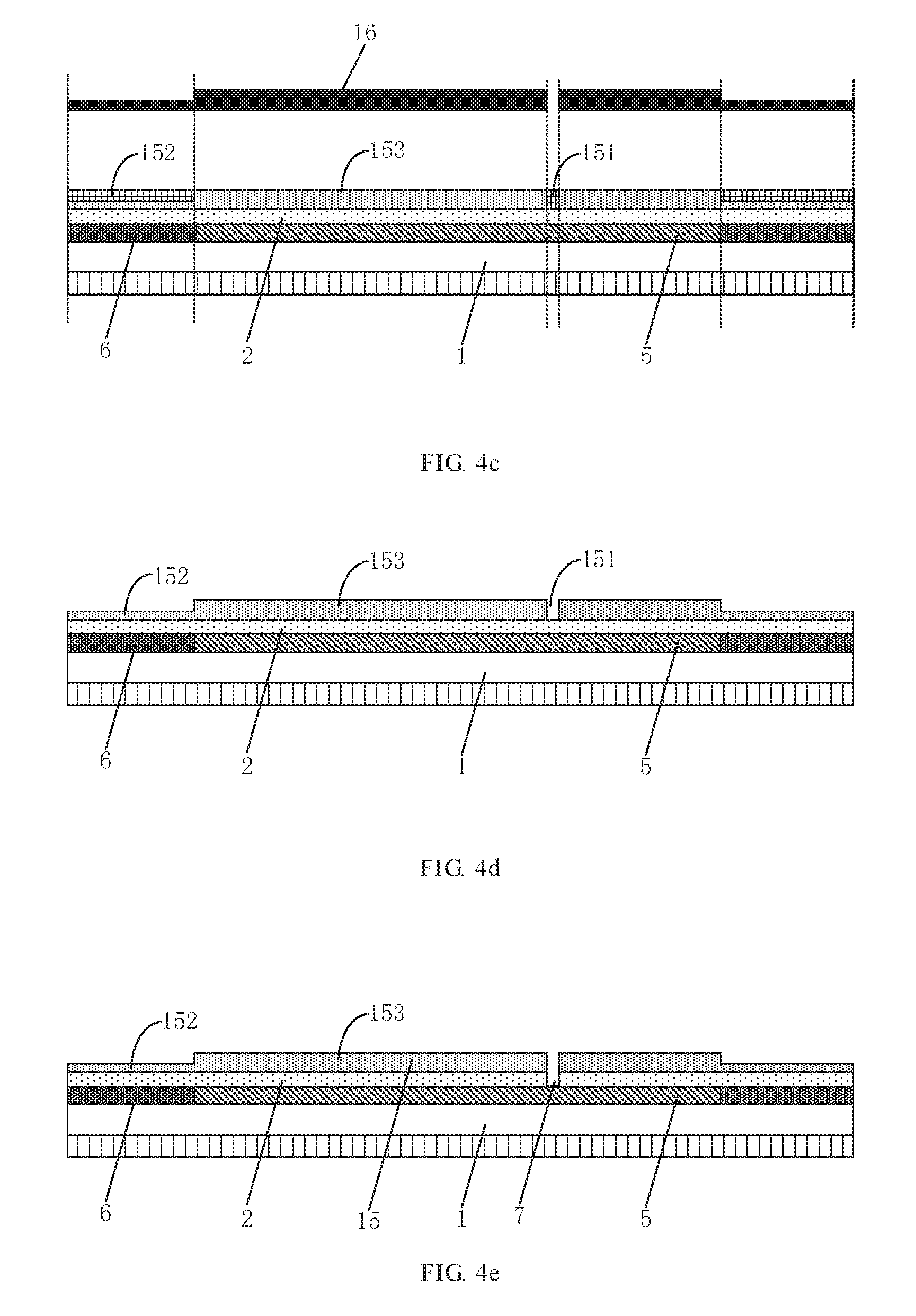
[0086] In an embodiment, step 10 may further include step 101 of forming a protection layer on the first base substrate.
[0087] FIG. 4a is a schematic diagram of forming a protection layer according to an embodiment. As shown in FIG. 4a, a protection layer 2 is formed on the first base substrate 1. In the embodiment, a metal pattern 5 and a gate drive circuit 6 are formed on the first base substrate 1, and the protection layer 2 may be formed on the metal pattern 5 and the gate drive circuit 6. In the embodiment, the metal pattern 5 is located in the display area, the gate drive circuit 6 is located in the peripheral area, and the metal pattern 5 and the gate drive circuit 6 may be formed in a same layer.
[0088] Step 10 may further include step 102 of forming a first resin pattern on the protection layer.
[0089] Step 102 may include steps 1021 to 1025.
[0090] At step 1021, a resin material layer is formed on the protection layer.
[0091] FIG. 4b is a schematic diagram of forming a resin material layer according to an embodiment. As shown in FIG. 4b, a resin material layer 15 is formed on the protection layer 2. In the present embodiment, the resin material layer 15 is formed of a photosensitive resin.
[0092] At step 1022, the resin material layer is exposed using a mask plate to form an exposure pattern, the exposure pattern includes a resin removed region, a resin partly remaining region, and a resin completely remaining region, and the resin partly remaining region includes a removable portion and a remaining portion.
[0093] FIG. 4c is a schematic diagram of exposing a resin material layer according to an embodiment. As shown in FIG. 4c, the resin material layer 15 is exposed using a mask plate 16 to form an exposure pattern including a resin removed region 151, a resin partly remaining region 152, and a resin completely remaining region 153. The part of the mask plate 16 corresponding to the peripheral area is a halftone mask (HTM for short), and the halftone mask is used to form the resin partly remaining region 152, and the remaining parts of the mask plate 16 are used to form the resin removed region 151 and the resin completely remaining region 153.
[0094] At step 1023, the exposure pattern is developed to remove the resin removed region and the removable portion of the resin partly remaining region.
[0095] FIG. 4d is a schematic diagram of developing an exposure pattern according to an embodiment. As shown in FIG. 4d, the exposure pattern is developed to remove the resin removed region 151 and the removable portion of the resin partly remaining region 152 that are exposed, and maintain the unexposed resin completely remaining region 153 and the unexposed portion (i.e., the remaining portion) of the resin partly remaining region 152.
[0096] At step 1024, a portion of the protection layer corresponding to the resin removed region that has been fully exposed is etched to form a via hole.
[0097] FIG. 4e is a schematic diagram of forming a via hole according to an embodiment. As shown in FIG. 4e, a portion of the protection layer 2 corresponding to the resin removed region 151 is etched to form a via hole 7. The remaining portion of the resin partly remaining region 152 in the peripheral area can ensure that a portion of the protection layer 2 located therebelow in the peripheral area is not etched off. The resin removed region 151 corresponds to the via hole 7.
[0098] At step 1025, the remaining portion of the resin partly remaining region is removed by an ashing process to expose the portion of the protection layer located in the peripheral area, and the resin completely remaining region is thinned to form a first resin pattern.
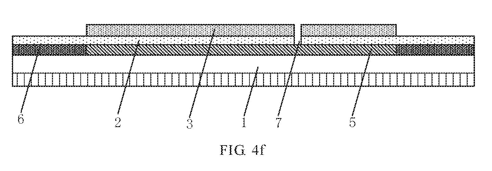
[0099] FIG. 4f is a schematic diagram of forming a first resin pattern according to an embodiment. As shown in FIG. 4f, an ashing process is performed such that the remaining portion of the resin partly remaining region 152 is removed to expose the portion of the protection layer 2 in the peripheral area and the resin completely remaining region 153 is thinned to form the first resin pattern 3. The resin completely remaining region 153 corresponds to the first resin pattern 3, and the resin partly remaining region 152 corresponds to the portion of the protection layer 2 in the peripheral area.
[0100] In this step, the remaining portion of the resin partly remaining region 152 and the resin completely remaining region 153 are thinned together by the ashing process, so that the remaining portion of the resin partly remaining region 152 is completely removed, and the resin completely remaining region 153 is thinned to form the first resin pattern 3.
[0101] In the method for manufacturing a display panel according to an embodiment of the present disclosure, the second resin pattern 8 may be formed by thinning the resin completely remaining region, the second resin pattern is located in a part of the peripheral area, the resin completely remaining region also corresponds to the second resin pattern, and the resin partly remaining region corresponds to a part, on which the second resin pattern is not formed, of the portion of the protection layer in the peripheral area.
[0102] In an embodiment, after step 102, the method may further include forming an electrode pattern (not shown) on the first resin pattern 3. A part of the electrode pattern is located in the via hole 7 and in contact with the exposed metal pattern 5, thereby achieving connection of the electrode pattern with the metal pattern 5.
[0103] The method for manufacturing the display panel according to the embodiment further includes step 20 of preparing an opposite substrate.
[0104] The method for manufacturing the display panel according to the embodiment further includes step 30 of arranging the display substrate and the opposite substrate to be opposite to each other and providing a sealant between the display substrate and the opposite substrate, and the sealant is provided in the peripheral area and in contact with the portion of the protection layer in the peripheral area.
[0105] In an embodiment, the sealant is formed on the entire portion of the protection layer in the peripheral area to contact with the entire portion of the protection layer in the peripheral area.
[0106] In another embodiment, the sealant is formed on the part, on which the second resin pattern is not formed, of the portion of the protection layer in the peripheral area and on the second resin pattern.
[0107] The method for manufacturing the display panel provided in this embodiment can be used to manufacture the display panel provided in the embodiments described with reference to FIG. 1. Detailed description of the display panel may refer to the embodiments described with reference to FIG. 1, and is not repeatedly given herein.
[0108] The method for manufacturing the display panel provided in this embodiment can also be used to manufacture the display panel provided in the embodiments described with reference to FIG. 2, and in this case, to manufacture the display panel in the embodiment shown in FIG. 2, it only needs to change the structure of the mask plate according to the structure of the product.
[0109] In the method for manufacturing the display panel provided by the embodiments, the first resin pattern is located in the display area, and the sealant is in contact with the portion of the protection layer in the peripheral area, so that the case where the sealant is only in contact with the resin layer in the peripheral area is avoided and the bonding force between the sealant and the display substrate is enhanced, thereby greatly reducing the undesirable phenomenon of peeling off of the sealant from the display substrate. The technical solutions according to the embodiments do not require significant modification to the structure and process of the existing display substrate, and no additional manufacturing equipment and process are required, thereby reducing manufacturing costs.
[0110] It should be understood that, the above embodiments are only exemplary embodiments for the purpose of explaining the principle of the present disclosure, but the present disclosure is not limited thereto. For one of ordinary skill in the art, various improvements and modifications may be made without departing from the spirit and essence of the present disclosure. These improvements and modifications also fall within the protection scope of the present disclosure.
* * * * *
D00000
D00001
D00002
D00003
D00004
XML
uspto.report is an independent third-party trademark research tool that is not affiliated, endorsed, or sponsored by the United States Patent and Trademark Office (USPTO) or any other governmental organization. The information provided by uspto.report is based on publicly available data at the time of writing and is intended for informational purposes only.
While we strive to provide accurate and up-to-date information, we do not guarantee the accuracy, completeness, reliability, or suitability of the information displayed on this site. The use of this site is at your own risk. Any reliance you place on such information is therefore strictly at your own risk.
All official trademark data, including owner information, should be verified by visiting the official USPTO website at www.uspto.gov. This site is not intended to replace professional legal advice and should not be used as a substitute for consulting with a legal professional who is knowledgeable about trademark law.