Phosphor, Method For Preparing Phosphor, Optoelectronic Component, And Method For Producing Optoelectronic Component
Rajendran; Veeramani ; et al.
U.S. patent application number 16/165954 was filed with the patent office on 2019-06-27 for phosphor, method for preparing phosphor, optoelectronic component, and method for producing optoelectronic component. This patent application is currently assigned to Everlight Electronics Co., Ltd.. The applicant listed for this patent is Everlight Electronics Co., Ltd.. Invention is credited to Ho Chang, Gabriel Nicolo A. De Guzman, Mu-Huai Fang, Shu-Fen Hu, Chieh-Yu Kang, Yan-Shen Lin, Ru-Shi Liu, Kuang-Mao Lu, Veeramani Rajendran.
| Application Number | 20190194539 16/165954 |
| Document ID | / |
| Family ID | 64426782 |
| Filed Date | 2019-06-27 |


View All Diagrams
| United States Patent Application | 20190194539 |
| Kind Code | A1 |
| Rajendran; Veeramani ; et al. | June 27, 2019 |
PHOSPHOR, METHOD FOR PREPARING PHOSPHOR, OPTOELECTRONIC COMPONENT, AND METHOD FOR PRODUCING OPTOELECTRONIC COMPONENT
Abstract
The present invention relates to a phosphor, a method for preparing the phosphor, an optoelectronic component, and a method for producing the optoelectronic component. The phosphor has the following general formula: La.sub.3(1-x)Ga.sub.1-yGe.sub.5(1-z)O.sub.16: 3xA.sup.3+, yCr.sup.3+, 5zB.sup.4+, where x, y, and z do not equal to 0 simultaneously; A represents at least one of Gd and Yb; B represents at least one of Sn, Nb, and Ta. For the phosphor, its emission spectrum is within a red visible light region and a near-infrared region when excited by blue visible light, purple visible light or ultraviolet light; and it has a wide reflection spectrum and a high radiant flux. Therefore, it can be used in optoelectronic components such as LEDs to meet requirements of current medical testing, food composition analysis, security cameras, iris/facial recognition, virtual reality, gaming notebook and light detection and ranging applications.
| Inventors: | Rajendran; Veeramani; (Madurai, IN) ; Fang; Mu-Huai; (Taoyuan City, TW) ; Liu; Ru-Shi; (Taipei, TW) ; Chang; Ho; (New Taipei City, TW) ; Lu; Kuang-Mao; (New Taipei City, TW) ; Lin; Yan-Shen; (New Taipei City, TW) ; Kang; Chieh-Yu; (New Taipei City, TW) ; De Guzman; Gabriel Nicolo A.; (Laguna, PH) ; Hu; Shu-Fen; (Taipei, TW) | ||||||||||
| Applicant: |
|
||||||||||
|---|---|---|---|---|---|---|---|---|---|---|---|
| Assignee: | Everlight Electronics Co.,
Ltd. New Taipei City TW |
||||||||||
| Family ID: | 64426782 | ||||||||||
| Appl. No.: | 16/165954 | ||||||||||
| Filed: | October 19, 2018 |
Related U.S. Patent Documents
| Application Number | Filing Date | Patent Number | ||
|---|---|---|---|---|
| 62608969 | Dec 21, 2017 | |||
| 62637788 | Mar 2, 2018 | |||
| Current U.S. Class: | 1/1 |
| Current CPC Class: | H01L 33/486 20130101; H01L 33/502 20130101; C09K 11/7708 20130101; C09K 11/62 20130101; H01L 33/005 20130101; C09K 11/7775 20130101; C09K 11/7766 20130101; H01L 2933/0041 20130101; C09K 11/66 20130101; C09K 11/7707 20130101; C09K 11/77 20130101; H01L 33/501 20130101; C09K 11/7776 20130101 |
| International Class: | C09K 11/77 20060101 C09K011/77; H01L 33/50 20060101 H01L033/50 |
Claims
1. A phosphor comprising the following general formula: La.sub.3(1-x)Ga.sub.1-yGe.sub.5(1-z)O.sub.16: 3xA.sup.3+, yCr.sup.3+, 5zB.sup.4+, wherein x, y, and z do not equal to 0 simultaneously; A represents at least one of Gd and Yb; and B represents at least one of Sn, Nb, and Ta.
2. The phosphor according to claim 1, wherein03x0.3,0y.ltoreq.0.2, 05z0.2.
3. The phosphor according to claim 1, further comprising the following general formula: La.sub.3Ga.sub.1-yGe.sub.5O.sub.16: yCr.sup.3+, wherein 0<y0.2.
4. The phosphor according to claim 1, further comprising the following general formula: La.sub.3(1-x)Ga.sub.1-yGe.sub.5O.sub.16: 3xA.sup.3+, yCr.sup.3+, wherein 03x0.3, 0y.ltoreq.0.2, and x and y do not equal to 0 simultaneously.
5. The phosphor according to claim 1, further comprising at least one of the following conditions based on the composition of La.sub.3GaGe.sub.5O.sub.16: Cr.sup.3+ replaces part of Ga.sup.3+; A.sup.3+ replaces part of La.sup.3+; B.sup.4+ replaces part of Ge.sup.4+.
6. The phosphor according to claim 1, further emitting light in a range of 600-1500 nm when excited by the excitation light having a wavelength of 400-500 nm.
7. The phosphor according to claim 6, further emitting the light comprising a radiant flux 4-70 mW.
8. The phosphor according to claim 1, being prepared by a method comprising steps of: Weighting the stating precursors selecting from oxide or carbonate containing materials and mixing raw materials for providing elements in the general formula according to the general formula of the phosphor, then sintering at a temperature of 1200-1500.degree. C. to obtain the phosphor
9. The phosphor according to claim 1, being prepared by a method comprising steps of: Preparing and mixing raw materials for providing elements in the general formula according to the general formula of the phosphor, then sintering at a temperature of 1200-1500.degree. C. to obtain the phosphor.
10. An optoelectronic component, comprising: a semiconductor chip for emitting excitation light during operation of the optoelectronic component; and a conversion unit provided with the phosphor according to claim 1 for converting the excitation light into emitted light.
11. The optoelectronic component according to claim 10, wherein the excitation light has a wavelength of 450 nm or 460 nm, and the emitted light has a wavelength of 650-1050 nm.
12. The optoelectronic component according to claim 10, wherein the semiconductor chip is a blue LED chip.
13. A method for producing an optoelectronic component, comprising steps of: producing a conversion unit on which the phosphor according to claim 1 is provided; and mounting the conversion unit on a semiconductor chip, wherein the semiconductor chip is used to generate excitation light during operation of the optoelectronic component.
Description
TECHNICAL FIELD
[0001] The present application relates to a phosphor, a method for preparing the phosphor, an optoelectronic component, and a method for producing the optoelectronic component, in particular, it relates to a phosphor having a high radiant flux and having a wide emission spectral wavelength in a red visible light and near-infrared regions, a method for preparing the phosphor, an optoelectronic component provided with the phosphor, and a process for producing the optoelectronic component.
BACKGROUND
[0002] Visible light is a part of the electromagnetic spectrum that can be perceived by human eyes. Infrared light is an electromagnetic wave (light) having a longer wavelength than the visible light. Studies have shown that infrared light can "penetrate" into human skin and is absorbable by the epidermis, dermis and subcutaneous tissue. At the same time, some spectrums absorbable by human organs falls within a visible range of electromagnetic spectrum, however, the reflected spectrum is a broadband reflection spectrum, which is within ranges of near-infrared light and red visible light. For instance, in a human brain, protein and oxyhemoglobin have an absorption spectrum and a reflection spectrum of 450 nm-600 nm and 700 nm-900 nm, respectively.
[0003] Therefore, organs can be detected according to the light spectrum absorbed or reflected by the different organs of the human body, for instance, for analyzing haemoglobin content, oxygen saturation, scattering lipid content, etc., and an extension has been made to the field of food or polymer component detection. In recent years, an optoelectronic component capable of generating a wide infrared emission spectrum has been widely used in security camera, iris/facial recognition, virtual reality, gaming notebook and light detection and ranging (LIDAR) technologies.
[0004] However, the infrared light emitted by optoelectronic components on the current market has disadvantages such as narrow emission spectrum, low radiant flux and the like, which cannot meet application requirements of the above medical component detection, intelligent technology and the like.
[0005] A luminescent material is a material that releases energy in the form of emitted light due to excitation from excitation light source. Currently, the luminescent material that is most studied and well-developed is mainly phosphor, especially phosphor excited by the blue chip for generating white LEDs, and the research has a focus on how to obtain emitted light (or called a secondary radiation) of a narrower wavelength range. The principle of white LED applies to the infrared phosphors converted LED also and hence it possesses advantages like low power consumption, compact, high lifetime and cheaper as compared to traditional light sources. In recent research, it is also reported that the use of phosphor is expanded to the security of anti-counterfeit and marker identification. For instance, it is reported that a study is made on the possibility of La.sub.3Ga.sub.5GeO.sub.14: Cr.sup.3+ for the applications of persistent luminescence, which mainly utilizing the phosphorescence property of the phosphors, continuous emission of light for a long time after excitation is ceased off. However, there is no report about the phosphor which can produce wide red visible light and near-infrared spectrums when excited by blue visible light, purple visible light or ultraviolet light and has a high radiant flux, let alone its application in the optoelectronic component.
SUMMARY
[0006] In view of the above drawbacks in the prior art, the present application provides a phosphor capable of emitting near-infrared light and red visible light when excited by blue visible light, purple visible light or ultraviolet light and having a wide emission spectrum and a high radiant flux.
[0007] The present application further provides a method for preparing the above phosphor, the phosphor prepared by the method can emit near-infrared light and red visible light when excited by blue visible light, purple visible light or ultraviolet light, and has a wide emission spectrum and a high radiant flux.
[0008] The present application provides an optoelectronic component, which can use a conversion unit provided with the above phosphor to convert blue visible light, purple visible light or ultraviolet light emitted from a semiconductor chip into the near-infrared light and red visible light. The optoelectronic component has a wide emission spectrum and a high radiant flux in the ranges of near-infrared light and red visible light.
[0009] The present application further provides a method for producing an optoelectronic component, where the method has a characteristic of simple process and can produce an optoelectronic component that converts blue visible light, purple visible light or ultraviolet light into the near-infrared light and red visible light.
[0010] To achieve the above purpose, the present application provides a phosphor having the following general formula:
[0011] (General Formula I) La.sub.3(1-x)Ga.sub.1-yGe.sub.5(1-z)O.sub.16: 3xA.sup.3+, yCr.sup.3+, 5zB.sup.4+, where x, y, and z do not equal to 0 simultaneously; A represents at least one of Gd and Yb; and B represents at least one of Sn, Nb, and Ta.
[0012] The phosphor is composed of a host material acting as a matrix and a dopant (or referred to as a luminescent center) acting as an activator, sometimes a sensitizer needs to be incorporated. The activator and the sensitizer replacing the ions in the original site of the matrix lattice.
[0013] Specifically, in the phosphor represented by the General Formula I, 0.times.0.5, 0 y.ltoreq.0.5, 0z.ltoreq.z0.5, and x, y, and z do not equal to 0 simultaneously. In a specific implementation of the present application, usually 03x0.3, 0y.ltoreq.0.2, 05z0.2, and x, y and z do not equal to 0 simultaneously.
[0014] In a specific implementation of the present application, the phosphor has the following general formula:
La.sub.3Ga.sub.1-yGe.sub.5O.sub.16: yCr.sup.3+, where 0<y0.2. (General Formula II)
[0015] In the phosphor represented by the General Formula II, La.sub.3Ga.sub.1-yGe.sub.5O.sub.16is a host material of the matrix, and Cr.sup.3+ is an activator. Adjusting the doping concentration of Cr.sup.3+, the emission spectrum of the phosphor is maintained in a near-infrared region and a red visible region, but the radiant flux changes accordingly; therefore, the doping concentration of Cr.sup.3+ is generally controlled to 0.5%-20%, it means, 0.005y.ltoreq.0.2. In a specific implementation of the present application, the doping concentration of Cr.sup.3+ is usually controlled to 3.0%-11%, it means, 0.035y<0.11, so that the phosphor has a high radiant flux.
[0016] In another implementation of the present application, the phosphor has the following general formula:
La.sub.3(1-x)Ga.sub.1-yGe.sub.5O.sub.16: 3xA.sup.3+, yCr.sup.3+, where 03x0.3, 0y.ltoreq.0.2, and x and y do not equal to 0 simultaneously, for instance, 03x0.3 and 0<y0.2; A represents at least one of Gd and Yb.
[0017] In the phosphor represented by the General Formula III, the doping concentration of Cr.sup.3+ is fixed. For instance, the doping concentration of Cr.sup.3+ is controlled to less than 10%, that is, 0<y0.1; changing the doping concentration of A.sup.3+, the emission spectrum of the phosphor is maintained at the near-infrared region and the red visible region, but the radiant flux changes accordingly, therefore, the doping concentration of A.sup.3+ is generally controlled to 0.1%-10%, that is, 0.0033x0.3. In a specific implementation of the present application, the doping concentration of A.sup.3+ is generally controlled to 0.5%-5%, that is, 0.0153x0.15, so that the phosphor has a high radiant flux.
[0018] In still another implementation of the present application, in the phosphor having the General Formula I (La.sub.3(1-x)Ga.sub.1-yGe.sub.5(1-z)O.sub.16: 3xA.sup.3+, yCr.sup.3+, 5zB.sup.4+), 0<3x0.3, 0<y0.2, 0<5z0.2; A represents at least one of Gd and Yb; and B represents at least one of Sn, Nb and Ta.
[0019] In the phosphor represented by the General Formula I, the doping concentrations of Cr.sup.3+ and A.sup.3+ are fixed. For instance, it is controlled that 0<3x0.1, 0y0.1; changing the doping concentration of B.sup.4+, the emission spectrum of the phosphor is maintained in the near-infrared region and the red visible region, but the radiant flux changes accordingly, therefore, the doping concentration of B.sup.4+ is generally controlled to 0.5%-4%, that is, 0.025.ltoreq.5z0.2. In a specific implementation process of the present application, the doping concentration of B.sup.4+ is generally controlled to 0.5%-3%, that is, 0.0255z0.15, so that the phosphor has a high radiant flux.
[0020] Specifically, the above phosphor satisfies at least one of the following three conditions based on the composition of La.sub.3GaGe.sub.5O.sub.16:
[0021] Cr.sup.3+ replaces part of Ga.sup.3+;
[0022] A.sup.3+ replaces part of La.sup.3+;
[0023] B.sup.4+ replaces part of Ge.sup.4+.
[0024] For instance, for the phosphor represented by the General Formula II, the doped Cr.sup.3+ replaces part of Ga.sup.3+ in the matrix La.sub.3GaGe.sub.5O.sub.16, or the incorporation of Cr.sup.3+ to replace Ga.sup.3+ on the original site of the matrix lattice.
[0025] When excited by blue visible light, purple visible light or ultraviolet light acting as a primary radiation, the above phosphor emits a secondary radiation within the ranges of the red visible light spectrum and the near-infrared spectrum and has a wide emission spectrum. In particular, the above phosphor has an emission spectrum of 650 -1500 nm, especially 650-1050 nm, when excited by excitation light having a wavelength of 400-500 nm, especially a wavelength of 450 nm or 460 nm.
[0026] Moreover, the phosphor has a high radiant flux within the range of the emission spectrum described above, and radiant flux of the light emitted by the phosphor is 4-70 mW.
[0027] In still another implementation of the present application, a phosphor having the following general formula is provided:
La.sub.3Ga.sub.5(1-x)Ge.sub.1-yO.sub.14: 5xCr.sup.3+, ySn.sup.4+, where 0x.ltoreq.0.1, 0y.ltoreq.0.9.
[0028] In the phosphor represented by the General Formula IV, La.sub.3Ga.sub.5(1-x)Ge.sub.1-yO.sub.14 is used as a host material of the matrix, Cr.sup.3+ is used as an activator (or called a luminescent center), and Sn.sup.4+ is used as a sensitizer.
[0029] When excited by blue visible light, purple visible light or ultraviolet light acting as a primary radiation, the phosphor represented by the General Formula IV emits a secondary radiation within the ranges of the red visible light spectrum and the near-infrared spectrum and has a wide emission spectrum. Specifically, when excited by excitation light having a wavelength of 400-500 nm, especially a wavelength of 450 nm or 460 nm, the phosphor represented by the General Formula IV has an emission spectrum of 650-1500 nm, especially 650-1050 nm.
[0030] Specifically, based on the La.sub.3Ga.sub.5GeO.sub.14 composition, in the phosphor represented by the General Formula IV, Cr.sup.3+ and Sn.sup.4+ partially replace the part of metal elements in the host material.
[0031] All of the above phosphors can be prepared by a conventional high-temperature solid-state reaction method in the art. Specifically, raw materials are stoichiometrically weighted according to the above general formula and mixed evenly in an agate mortar and then sintered at a certain temperature in the furnace, for instance, at a temperature of 1200-1500.degree. C. to obtain a target product.
[0032] The present application further provides a method for preparing the above-described phosphor, including steps of preparing and mixing raw materials for providing elements in the general formula according to the general formula of the luminescent material and then sintering at a temperature of 1200-1500.degree. C. to obtain a target phosphor.
[0033] Specifically, the raw materials are accurately weighed according to a designed formula, placed in an agate mortar to grind for evenly mixing, and then the mixture is sintered in an air atmosphere, generally, the temperature is controlled to 1250-1350.degree. C. to sinter for about 5-6 hours, then the phosphor can be obtained.
[0034] The raw materials for preparing the phosphor described above may be specifically selected from oxide or carbonate containing the elements in the determined general formula or other compounds capable of providing corresponding metal elements. For instance, if the phosphor to be prepared has a molecular formula of La.sub.3Ga.sub.0.09Ge.sub.5O.sub.16:0.01Cr.sup.3+, then a weighted calculation may be performed for the desired raw materials La.sub.2O.sub.3, Ga.sub.2O.sub.3, Cr.sub.2O.sub.3 and GeO.sub.2 according to a stoichiometric ratio in the molecular formula, and the weights of the raw materials are finally determined.
[0035] The present application provides an optoelectronic component including:
[0036] a semiconductor chip for emitting excitation light during operation of the optoelectronic component; and
[0037] a conversion unit provided with the above-described phosphor for converting the excitation light into emitted light.
[0038] Specifically, the excitation light acting as the primary radiation has a wavelength of 400-500 nm, especially a wavelength of 450 nm or 460 nm; the emitted light acting as the secondary radiation has a wavelength of 600-1500 nm, especially 600-1100 nm, and more particularly 650-1050 nm.
[0039] The above semiconductor chip is not particularly limited in the present application, as long as it can emit the primary radiation of the above wavelength during operation, such as a blue, purple or ultraviolet LED chip or laser chip which has been commercialized, especially a blue LED chip of 400-500 nm, more particularly a blue LED chip of 450 nm or a blue LED chip of 460 nm. In a specific implementation of the present application, a blue LED chip having an emission wavelength of 450-452.5 nm is used.
[0040] The above-described optoelectronic component is not particularly limited in the present application with regard to its specific form, as long as it can achieve the above functions. For instance, it may present in a form of an LED device including at least a blue, purple or ultraviolet LED chip for generating a primary radiation and a conversion unit for converting the primary radiation into a secondary radiation. The conversion unit is disposed in an optical path of the primary radiation and contains or is provided with the above-described phosphor.
[0041] The present application does not specifically limit how to obtain the conversion unit according to the above phosphor. It can be a common method in the field of optoelectronic components, especially LED devices, as long as a cooperation with the LED chip may be achieved to realize the conversion from the primary radiation to the secondary radiation. For instance, the phosphor is dispersed in a transparent epoxy resin in a certain ratio to obtain a conversion unit dispersed outside the LED chip.
[0042] The present application further provides a method for producing an optoelectronic component, including steps of:
[0043] producing a conversion unit on which the above phosphor is provided;
[0044] mounting the produced conversion unit on a semiconductor chip, where the semiconductor chip is used to generate excitation light during operation of the optoelectronic component.
[0045] The closer the phosphor is to the semiconductor chip, the higher or the lower its concentration is.
[0046] The closer the phosphor is to the semiconductor chip, the higher or the lower its concentration appears in a gradient manner.
[0047] The phosphor may be in direct or indirect contact with the semiconductor chip.
[0048] The phosphor may be a quantum dot phosphor.
[0049] Particles of the phosphor may be covered with at least one layer of oxide at its periphery, such as silicon dioxide.
[0050] Further, the method for producing the optoelectronic component described above may further include step for preparing the above-described phosphor: preparing and mixing the raw materials for providing elements in the general formula according to the general formula of the phosphor, and then sintering at a temperature of 1200-1500.degree. C., for instance, sintering for about 5-6 hours at a temperature of about 1250-1350.degree. C. to obtain the desired phosphor.
[0051] For the phosphor provided in the present application, its emission spectrum is within the red visible light and near-infrared light when excited by blue visible light, purple visible light or ultraviolet light; and it has a wide emission spectrum and a high radiant flux. Therefore, it can be used in optoelectronic components such as LEDs and laser devices to meet requirements of current medical testing, food composition analysis, security camera, iris/facial recognition, virtual reality, gaming notebook and light detection and ranging applications.
[0052] The preparing method of the above phosphor provided in the present application has a characteristic of the simple process and is convenient for practical generalization and large-scale application.
[0053] The optoelectronic component provided in the present application can use a conversion unit provided with the above-described phosphor to convert blue, purple or ultraviolet light emitted from the semiconductor chip into near-infrared light and red visible light in order , and it has a wide emission spectrum and a high radiation flux in the ranges of near-infrared light and red visible light, so as to meet requirements of current medical testing, food composition analysis, security cameras, iris/facial recognition, virtual reality, gaming notebook and light detection and ranging applications.
[0054] Moreover, the optoelectronic component has a characteristic of the simple structure, can be improved and obtained on the basis of the existing optoelectronic component, and has an advantage of low manufacturing cost.
[0055] The method for producing the optoelectronic component provided in the present application has a characteristic of simple process and can be processed on the basis of the existing device component, further facilitating the generalization of the above-described optoelectronic component.
BRIEF DESCRIPTION OF DRAWING(S)
[0056] FIG. 1 is the X-ray diffraction spectrum of the phosphor La.sub.3Ga.sub.0.99Ge.sub.5O.sub.16: 0.01Cr.sup.3+ according to Example 1;
[0057] FIG. 2 is the X-ray diffraction spectrum of the phosphor La.sub.3Ga.sub.0.93Ge.sub.5O.sub.16: 0.07Cr.sup.3+ according to Example 1;
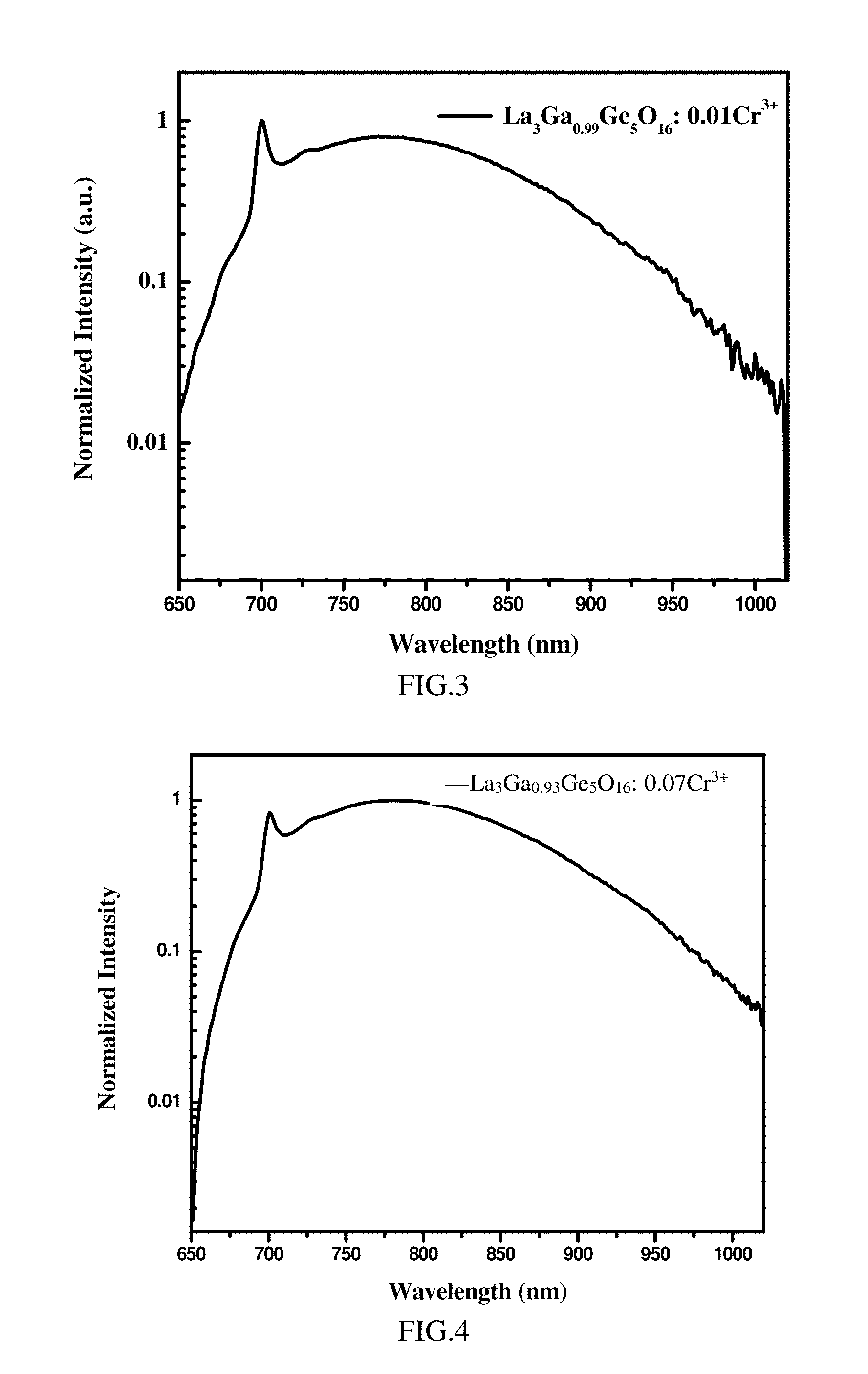
[0058] FIG. 3 is the photoluminescence emission spectrum (the excitation light has a wavelength of 460 nm) of the phosphor La.sub.3Ga.sub.0.99Ge.sub.5O.sub.16: 0.01Cr.sup.3+ according to Example 1;
[0059] FIG. 4 is the photoluminescence emission spectrum (the excitation light has a wavelength of 450 nm) of the phosphor La.sub.3Ga.sub.0.93Ge.sub.5O.sub.16: 0.07Cr.sup.3+ according to Example 1;
[0060] FIG. 5 is the X-ray diffraction spectrum of the phosphor La.sub.2.97Ga.sub.0.99Ge.sub.5O.sub.16: 0.03Gd.sup.3+, 0.01Cr.sup.3+ according to Example 2;
[0061] FIG. 6 is the photoluminescence emission spectrum (the excitation light has a wavelength of 460 nm) of the phosphor La.sub.2.97Ga.sub.0.99Ge.sub.5O.sub.16: 0.03Gd.sup.3+, 0.01Cr.sup.3+ according to Example 2;
[0062] FIG. 7 is the X-ray diffraction spectrum of the phosphor La.sub.2.97Ga.sub.0.99Ge.sub.5O.sub.16: 0.03Yb.sup.3+, 0.01Cr.sup.3+ according to Example 3;
[0063] FIG. 8 is the photoluminescence emission spectrum (the excitation light has a wavelength of 460 nm) of the phosphor La.sub.2.97Ga.sub.0.99Ge.sub.5O.sub.16: 0.03Yb.sup.3+, 0.01Cr.sup.3+ according to Example 3;
[0064] FIG. 9 is the X-ray diffraction spectrum of the phosphors according to Examples 4-5;
[0065] FIG. 10 is the photoluminescence emission spectrum (the excitation light has a wavelength of 450 nm) of the phosphor La.sub.2.97Ga.sub.0.93Ge.sub.5O.sub.16: 0.03Gd.sup.3+, 0.07Cr.sup.3+ according to Example 4;
[0066] FIG. 11 is the photoluminescence emission spectrum (the excitation light has a wavelength of 450 nm) of the phosphor La.sub.2.97Ga.sub.0.93Ge.sub.4.95O.sub.16: 0.03Gd.sup.3.+-., 0.07Cr.sup.3+, 0.05Sn.sup.4+ according to Example 5;
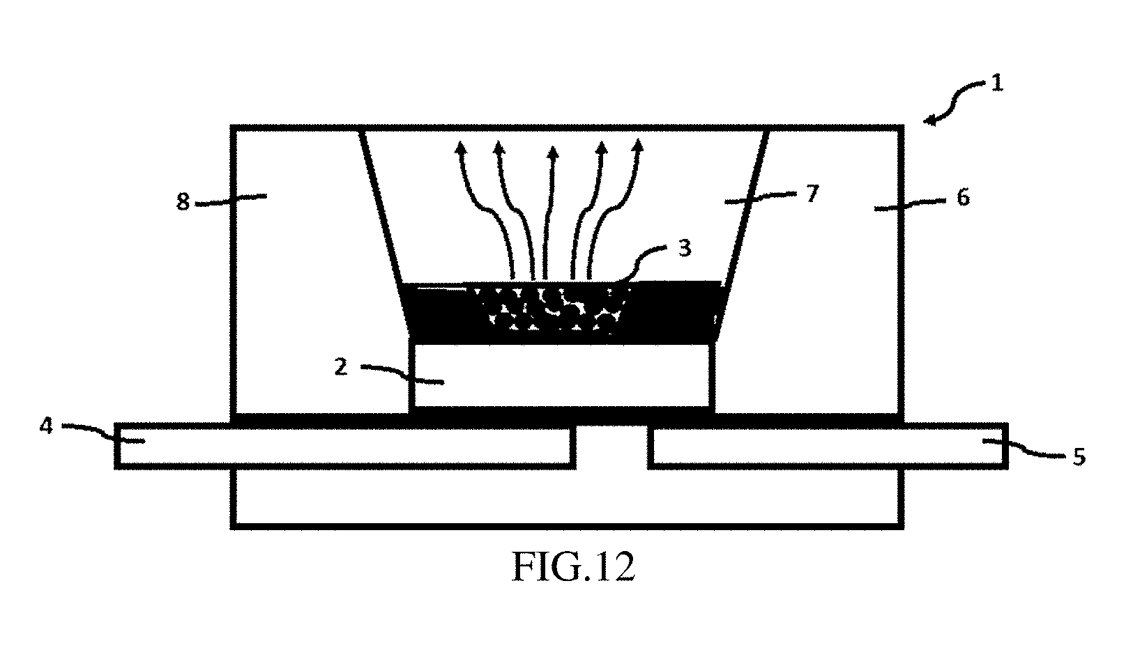
[0067] FIG. 12 is a schematic structural diagram of the optoelectronic component according to Example 6;
[0068] FIG. 13 is the photoluminescence emission spectrum (the excitation light has a wavelength of 450 nm) of the phosphor having different doping concentrations of Cr.sup.3+ according to Experimental Example 1;
[0069] FIG. 14 is a graph showing the relationship between the doping concentration of Cr.sup.3+ and the radiant flux according to Experimental Example 1;
[0070] FIG. 15 is the photoluminescence emission spectrum (the excitation light has a wavelength of 450 nm) of the phosphor having different doping concentrations of Gd.sup.3+ according to Experimental Example 2;
[0071] FIG. 16 is a graph showing the relationship between the doping concentration of Gd.sup.3+ and the radiant flux according to Experimental Example 2;
[0072] FIG. 17 is the photoluminescence emission spectrum (excitation light has a wavelength of 450 nm) of the phosphor having different doping concentrations of Sn.sup.4+ according to Experimental Example 3;
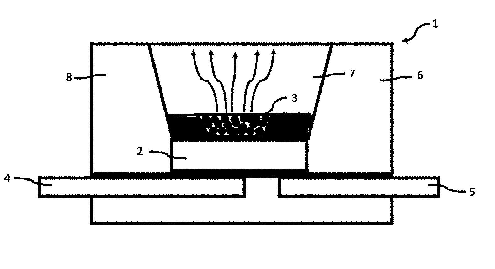
[0073] FIG. 18 is a graph showing the relationship between the doping concentration of Sn.sup.4+ and the radiant flux according to Experimental Example 3;
[0074] FIG. 19 is the photoluminescence emission spectrum (the excitation light has a wavelength of 450 nm) of the La.sub.3Ga.sub.0.99Ge.sub.5O.sub.16: 0.01Cr.sup.3+ and La.sub.3Ga.sub.4.95Ge.sub.0.9O.sub.14: 0.05Cr.sup.3+ according to Comparative Example 1;
[0075] FIG. 20 is the X-ray diffraction spectrum of the phosphor according to Example 7;
[0076] FIG. 21 is the photoluminescence emission spectrum (the excitation light has a wavelength of 460 nm) of the phosphor according to Example 7;
[0077] FIG. 22 is the X-ray diffraction spectrum of the phosphor La.sub.3Ga.sub.4.95Ge.sub.0.9O.sub.14: 0.05Cr.sup.3+, 0.1Sn.sup.4+ according to Example 8;
[0078] FIG. 23 is the X-ray diffraction spectrum of the phosphor La.sub.3Ga.sub.4.95Ge.sub.0.7O.sub.14: 0.05Cr.sup.3+, 0.3Sn.sup.4+ according to Example 8;
[0079] FIG. 24 is the X-ray diffraction spectrum of the phosphor La.sub.3Ga.sub.4.95Ge.sub.0.5O.sub.14: 0.05Cr.sup.3+, 0.5Sn.sup.4+ according to Example 8;
[0080] FIG. 25 is the photoluminescence emission spectrum (the excitation light has a wavelength of 460 nm) of the phosphor La.sub.3Ga.sub.4.95Ge.sub.0.9O.sub.14: 0.05Cr.sup.3+, 0.1Sn.sup.4+ according to Example 8;
[0081] FIG. 26 is the photoluminescence emission spectrum (the excitation light has a wavelength of 460 nm) of the phosphor La.sub.3Ga.sub.4.95Ge.sub.0.7O.sub.14: 0.05Cr.sup.3+, 0.3Sn.sup.4+ according to Example 8;
[0082] FIG. 27 is the photoluminescence emission spectrum (the excitation light has a wavelength of 460 nm) of the phosphor La.sub.3Ga.sub.4.95Ge.sub.0.5O.sub.14: 0.05Cr.sup.3+, 0.5Sn.sup.4+ according to Example 8; and
[0083] FIG. 28 is a schematic structural diagram of the optoelectronic component according to Example 9 of the present application.
DETAILED DESCRIPTION
[0084] In order to describe objectives, technical solutions and advantages of examples of the present application more clearly, the technical solutions in the examples of the present application will be described hereunder clearly and completely with reference to the accompanying drawings in the examples of the present application. The described examples are only a part of examples, rather than all examples of the present application. All other examples obtained by those skilled in the art based on the embodiments of the present application without any creative effort should fall within the scope of the present application.
[0085] The raw materials used in the following examples: La.sub.2O.sub.3, Ga.sub.2O.sub.3 and Cr.sub.2O.sub.3 have a purity of 99.9% respectively, all of which are commercially available from Merck; GeO.sub.2 has a purity of 99.9%, which is commercially available from Aldrich; Gd.sub.2O.sub.3, Yb.sub.2O.sub.3 and SnO.sub.2 have a purity of 99.9% respectively, all of which are commercially available from Sigma Aldrich.
[0086] The tubular and muffle furnace is commercially available from Eurotherm. The
[0087] X-ray diffraction spectrum of the sample powders of the phosphor is measured by an X-ray diffractometer commercially available from BRUKER AXS with a model number of Desktop Bruker D2 PHASER A26-X1-A2B0B2A (Serial No. 205888). The photoluminescence emission spectrum of the sample powders of the phosphor is measured by Gemini 180 and iR320 commercially available from Horiba (Jobin Yvon).
EXAMPLE 1
[0088] The present example provides a set of phosphors having a general formula of La.sub.3Ga.sub.1-yGe.sub.5O.sub.16: yCr.sup.3+, where 0<y0.2, the chemical formulas of the set of phosphors are as follows:
[0089] La.sub.3Ga.sub.0.995Ge.sub.5O.sub.16: 0.005Cr.sup.3+
[0090] La.sub.3Ga.sub.0.99Ge.sub.5O.sub.16: 0.0 1Cr.sup.3+
[0091] La.sub.3Ga.sub.0.97Ge.sub.5O.sub.16: 0.03Cr.sup.3+
[0092] La.sub.3Ga.sub.0.95Ge.sub.5O.sub.16: 0.05Cr.sup.3+
[0093] La.sub.3Ga.sub.0.93Ge.sub.5O.sub.16: 0.07Cr.sup.3+
[0094] La.sub.3Ga.sub.0.91Ge.sub.5O.sub.16: 0.09Cr.sup.3+
[0095] La.sub.3Ga.sub.0.89Ge.sub.5O.sub.16: 0.11Cr.sup.3+
[0096] La.sub.3Ga.sub.0.87Ge.sub.5O.sub.16: 0.13Cr.sup.3+
[0097] The preparing method of the set of phosphors is as follows: according to stoichiometric ratios in the molecular formulae of the phosphors, accurately weighing the raw materials La.sub.2O.sub.3, Ga.sub.2O.sub.3, GeO.sub.2 and Cr.sub.2O.sub.3; placing the weighed raw materials in an agate mortar to grind for evenly mixing; then transferring the resulting mixture to an alumina crucible; placing in a muffle furnace and sintering in an air atmosphere at a temperature of about 1250-1300.degree. C. for about 5-6 hours; and after cooling with the furnace, grinding into powders to obtain a target phosphor.
[0098] FIG. 1 and FIG. 2 shows the X-ray diffraction spectrums of La.sub.3Ga.sub.0.99Ge.sub.5O.sub.16: 0.01Cr.sup.3+ and La.sub.3Ga.sub.0.93Ge.sub.5O.sub.16: 0.07Cr.sup.3+, respectively. X-ray diffraction spectrums of other phosphors in the set are similar to those in FIG. 1-FIG. 2. As shown in FIG. 1 and FIG. 2, the X-ray diffraction spectrum of the above two phosphors are respectively compared with a standard X-ray diffraction spectrum. All the diffraction peaks of the two phosphors are consistent with a standard spectrum JCPDS 890211 (ICSD-50521) and no impurity peak is observed, indicating that the incorporation of Cr.sup.3+ incurred no changes in the crystal structure, that is, the activator Cr.sup.3+ successfully entered into the crystal lattice. Further, the crystals of La.sub.3Ga.sub.0.99Ge.sub.5O.sub.16: 0.01Cr.sup.3+ and La.sub.3Ga.sub.0.93Ge.sub.5O.sub.16: 0.07Cr.sup.3+ belong to a triclinic system, and a space group is P-1(2).
[0099] FIG. 3 and FIG. 4 shows the photoluminescence emission spectrums of La.sub.3Ga.sub.0.99Ge.sub.5O.sub.16: 0.01Cr.sup.3+ and La.sub.3Ga.sub.0.93Ge.sub.5O.sub.16: 0.07Cr.sup.3+, respectively. The photoluminescence emission spectrums of other phosphors are similar to those in FIG. 3 and FIG. 4. As shown in FIG. 3 and FIG. 4, when excited by excitation light of 460 nm or 450 nm, the emission spectrums of La.sub.3Ga.sub.0.99Ge.sub.5O.sub.16: 0.01Cr.sup.3+ and La.sub.3Ga.sub.0.93Ge.sub.5O.sub.16: 0.07Cr.sup.3+ cover the spectral range of 600-1100 nm, especially a spectral range of 650-1050 nm.
[0100] Based on the above test and characterization results, considering the ionic radius and valence state, it can be determined that, in the set of phosphors, the incorporation of Cr.sup.3+ replaces the lattice position of Ga.sup.3+ in the matrix.
EXAMPLE 2
[0101] The present example provides a phosphor having a molecular formula of La.sub.2.97Ga.sub.0.99Ge.sub.5O.sub.16: 0.03Gd.sup.3+, 0.01Cr.sup.3+, the preparing method of the phosphor is as follows:
[0102] According to a stoichiometric ratio in the molecular formula of the phosphor, accurately weighing the raw materials La.sub.2O.sub.3, Ga.sub.2O.sub.3, GeO.sub.2, Gd.sub.2O.sub.3 and Cr.sub.2O.sub.3, and placing the weighed raw materials into an agate mortar to grind for evenly mixing; then transferring the mixture to an alumina crucible; placing in a muffle furnace and sintering in an air atmosphere; controlling the temperature at about 1250.degree. C. to sinter for about 6 hours; and after cooling in the furnace, grinding into powders to obtain the phosphor.
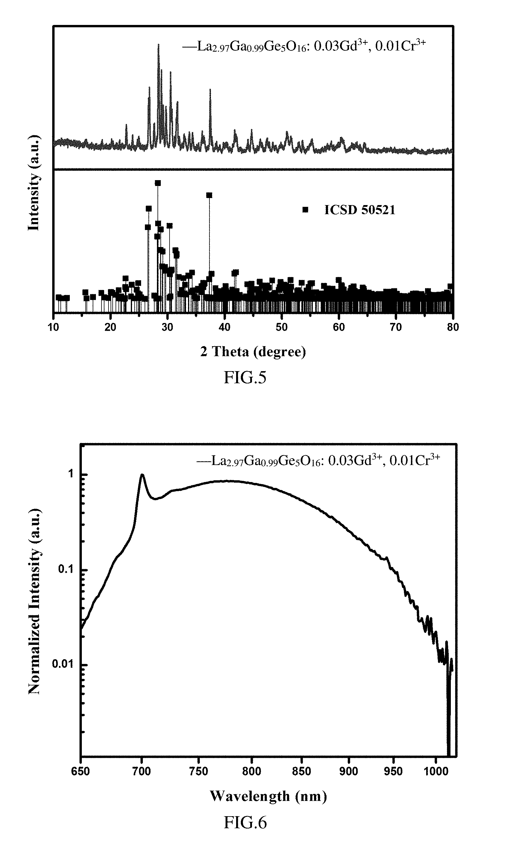
[0103] As shown in FIG. 5, the X-ray diffraction spectrum of the phosphor is compared with the standard X-ray diffraction spectrum. All the diffraction peaks of the phosphor are consistent with the standard spectrum JCPDS 890211 (ICSD-50521) and no impurity peak is detected, indicating that the activator Cr.sup.3+ and the sensitizer Gd.sup.3+ successfully entered into the crystal lattice. Further, the crystal of the phosphor belongs to the triclinic system, and the space group is P-1 (2).
[0104] As shown in FIG. 6, when excited by the excitation light of 460 nm, the emission spectrum of La.sub.2.97G.sub.0.99Ge.sub.5O.sub.16: 0.03Gd.sup.3+, 0.01Cr.sup.3+ covers a spectral range of 600-1100 nm, especially a spectral range of 650-1050 nm.
[0105] Based on the above test and characterization results, considering the ionic radius and valence state, it can be determined that, in the phosphor, the incorporation of Cr.sup.3+ replaces the lattice position of Ga.sup.3+ in the matrix; similarly, the co-doped Gd.sup.3+ replaces La.sup.3+ on the original site of the matrix lattice.
EXAMPLE 3
[0106] The present example provides a phosphor having a molecular formula of La.sub.2.97Ga.sub.0.99Ge.sub.5O.sub.16: 0.03Yb.sup.3+, 0.01Cr.sup.3+, the preparing method of the phosphor is as follows:
[0107] According to a stoichiometric ratio in the molecular formula of the phosphor, accurately weighing the raw materials La.sub.2O.sub.3, Ga.sub.2O.sub.3, GeO.sub.2, Yb.sub.2O.sub.3 and Cr.sub.2O, and placing the weighed raw materials into an agate mortar to grind for evenly mixing; then transferring the mixture to an alumina crucible; placing in a muffle furnace and sintering in an air atmosphere; controlling the temperature at about 1250.degree. C. to sinter for about 6 hours; and after cooling with the furnace, grinding into powders to obtain the phosphor.
[0108] As shown in FIG. 7, the X-ray diffraction spectrum of the phosphor was compared with a standard X-ray diffraction spectrum. All the diffraction peaks of the phosphor are consistent with the standard spectrum JCPDS 890211 (ICSD-50521) and no impurity peak is detected, indicating that the activator Cr.sup.3+ and the sensitizer Yb.sup.3+ successfully entered into the crystal lattice. Further, the crystal of the phosphor belongs to the triclinic system, and the space group is P-1 (2).
[0109] As shown in FIG. 8, when excited by the excitation light of 460 nm, the emission spectrum of the phosphor La.sub.2.97Ga.sub.0.99Ge.sub.5O.sub.16: 0.03Yb.sup.3+, 0.01Cr.sup.3+ covers a spectral range of 600-1100 nm, especially a spectral range of 650-1050 nm.
[0110] Based on the above test and characterization results, considering the ionic radius and valence state, it can be determined that Cr.sup.3+ replaces Ga.sup.3+ on the original site in the matrix lattice. Similarly, the co-doped Yb.sup.3+ replaces La.sup.3+ on the original site in the matrix lattice.
EXAMPLE 4
[0111] The present example provides a set of phosphors having a general formula of La.sub.3(1-x)Ga.sub.1-yGe.sub.5O.sub.16: 3xA.sup.3+, yCr.sup.3+,where 0<3x0.3, y=0.07, and A represents Gd, the chemical formulae of the set of phosphors are as follows, and reference may be made to Example 2 for the corresponding preparing method:
[0112] La.sub.2.985Ga.sub.0.93Ge.sub.5O.sub.16: 0.015Gd.sup.3+, 0.07Cr.sup.3+
[0113] La.sub.2.97Ga.sub.0.93Ge.sub.5O.sub.16: 0.03Gd.sup.3+, 0.07Cr.sup.3+
[0114] La.sub.2.955Ga.sub.0.93Ge.sub.5O.sub.16: 0.045Gd.sup.3+, 0.07Cr.sup.3+
[0115] La.sub.2.94Ga.sub.0.93Ge.sub.5O.sub.16: 0.06Gd.sup.3+, 0.07Cr.sup.3+
[0116] La.sub.2.91Ga.sub.0.93Ge.sub.5O.sub.16: 0.09Gd.sup.3+, 0.07Cr.sup.3+
[0117] La.sub.2.85Ga.sub.0.93Ge.sub.5O.sub.16: 0.15Gd.sup.3+, 0.07Cr.sup.3+
[0118] La.sub.2.79Ga.sub.0.93Ge.sub.5O.sub.16: 0.21Gd.sup.3+, 0.07Cr.sup.3+
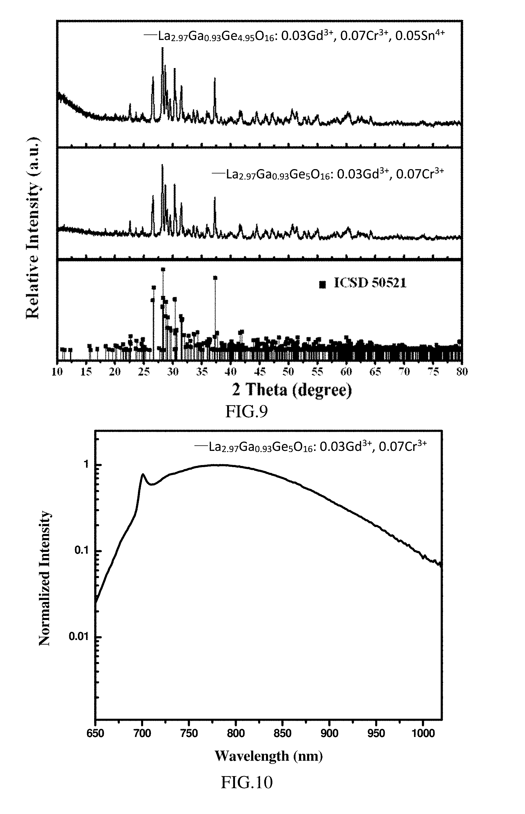
[0119] FIG. 9 is the X-ray diffraction spectrum of the phosphor La.sub.2.97Ga.sub.0.93Ge.sub.5O.sub.16: 0.03Gd.sup.3+, 0.07Cr.sup.3+, and XRD diffraction spectrums of other phosphors are similar to those in FIG. 9. As shown in FIG. 9, the X-ray diffraction spectrums of the phosphors are compared with the standard X-ray diffraction spectrum. All the diffraction peaks of the phosphors are consistent with the standard spectrum JCPDS 890211 (ICSD-50521), and no impurity peak is observed, indicating that the activator Cr.sup.3+ and the Gd.sup.3+ successfully entered into the crystal lattice. Further, the crystals of the set of phosphors belong to the triclinic system, and the space group is P-1 (2).
[0120] FIG. 10 is the photoluminescence emission spectrum of the phosphor La.sub.2.97Ga.sub.0.93Ge.sub.5O.sub.16: 0.03Gd.sup.3+, 0.07Cr.sup.3+. Photoluminescence emission spectrums of other phosphors are similar to those in FIG. 10. As shown in FIG. 10, when excited by the excitation light of 450 nm, the emission spectrum of the phosphor covers a range of 600-1100 nm, especially a range of 650-1050 nm.
[0121] Based on the above test and characterization results, considering the ionic radius and valence state, it can be determined that the incorporation of Cr.sup.3+ replaces Ga.sup.3+ on the original site in the matrix lattice. Similarly, the incorporation of co-doped Gd.sup.3+ replaces La.sup.3+ on the original site in the matrix lattice.
EXAMPLE 5
[0122] The present example provides a phosphor having a molecular formula of La.sub.2.97Ga.sub.0.93Ge.sub.4.95O.sub.16: 0.03Gd.sup.3+, 0.07Cr.sup.3+, 0.05Sn.sup.4+. The preparing method of the phosphor is as follows:
[0123] According to a stoichiometric ratio in the molecular formula of the phosphor, accurately weighing the raw materials La.sub.2O.sub.3, Ga.sub.2O.sub.3, GeO.sub.2, Gd.sub.2O.sub.3, Cr.sub.2O.sub.3 and SnO.sub.2, and placing the weighed raw materials into an agate mortar to grind for evenly mixing; then transferring the resulting mixture to an alumina crucible; placing in a muffle furnace and sintering in an air atmosphere; controlling the temperature at about 1250.degree. C. to sinter for about 5 hours; and after cooling with the furnace, grinding into powders to obtain the phosphor.
[0124] As shown in FIG. 9, the X-ray diffraction spectrums of the phosphors are compared with the standard X-ray diffraction spectrum. All the diffraction peaks of the phosphor are consistent with the standard spectrum JCPDS 890211 (ICSD-50521) and no impurity peak is observed, indicating that the activator Cr.sup.3+, the sensitizers Gd.sup.3+ and Sn.sup.4+ successfully entered into the crystal lattice. Further, the crystal of the phosphor belongs to the triclinic system, and the space group is P-1 (2).
[0125] As shown in FIG. 11, when excited by the excitation light of 450 nm, the emission spectrum of the phosphor covers a spectral range of 600-1100 nm, especially a spectral range of 650-1050 nm.
[0126] Based on the above test and characterization results, considering the ionic radius and valence state, it can be determined that the incorporation of Cr.sup.3+ replaces Ga.sup.3+ on the original site in the matrix lattice. Similarly, the incorporation of co-doped Gd.sup.3+ and Sn.sup.4+ replaces La.sup.3+ and Ge.sup.4+ on the original sites in the matrix lattice, respectively.
EXAMPLE 6
[0127] This example provides an optoelectronic component. As shown in FIG. 12, the optoelectronic component 1 includes a housing 6 provided with a recess 8, a semiconductor chip 2 for emitting a primary radiation, and a first lead 4 and a second lead 5 respectively connected to the a housing 6. An inner side wall of the recess 8 is coated with a suitable material to reflect the emitted light with the assistance of a reflector cup 7; the semiconductor chip 2 is mounted in the recess 8 and is respectively connected to the first lead 4 and the second lead 5 which are opaque;; a conversion unit 3 is mounted on an optical path of the primary radiation emitted from the semiconductor chip 2. The conversion unit 3 contains or is provided with the phosphor according to Examples 1-5 described above. Specifically, the phosphor is dispersed in the epoxy resin, and the conversion unit 3 is produced and dispersed outside the semiconductor chip 2 to absorb the primary radiation emitted from the semiconductor chip 2 and convert into a secondary radiation.
[0128] The basic parameters of the above optoelectronic component 1 are shown in Table 1; under these basic parameters, the measurement results of the radiant flux obtained when part of the phosphors in Examples 1-5 is used for the conversion unit 3 are shown in Table 2.
TABLE-US-00001 TABLE 1 LED Phosphor packaging Silicone content in the bracket LED chip specifications encapsulant conversion unit PPA3535 Size: 40 mil * 40 mil 1.4 Silicone 50 wt % Luminescence wavelength: 450-452.5 nm Power: 109.7 mW
TABLE-US-00002 TABLE 2 Radiant flux Phosphor chemical Total Radiant flux (.lamda. = formula radiant flux (.lamda. = 372-650 nm) 650-1050 nm) La.sub.3Ga.sub.0.99Ge.sub.5O.sub.16: 344.2 mW 326.8 mW 17.6 mW 0.01Cr.sup.3+ La.sub.2.97Ga.sub.0.99Ge.sub.5O.sub.16: 581.5 mW 558.8 mW 25.7 mW 0.03Gd.sup.3+, 0.01Cr.sup.3+ La.sub.2.97Ga.sub.0.99Ge.sub.5O.sub.16: 295.1 mW 286.0 mW 9.1 mW 0.03Yb.sup.3+, 0.01Cr.sup.3+ La.sub.3Ga.sub.0.93Ge.sub.5O.sub.16: 366.2 mW 323.1 mW 43.1 mW 0.07Cr.sup.3+ La.sub.2.97Ga.sub.0.93Ge.sub.5O.sub.16: 307.8 mW 251.5 mW 56.3 mW 0.07Cr.sup.3+, 0.03Gd.sup.3+ La.sub.2.67Ga.sub.0.93Ge.sub.4.95O.sub.16: 284.0 mW 218.8 mW 65.2 mW 0.07Cr.sup.3+, 0.03Gd.sup.3+, 0.05Sn.sup.4+
[0129] As can be seen from Table 2, the phosphor provided in the present application has a radiant flux of 4-70 mW in the wavelength range of 650-1050 nm and thus has a high radiant flux.
Experimental Example 1
[0130] The present experimental example aims to investigate the effects of different doping concentrations of Cr.sup.3+ on the radiant flux. Taking the phosphor having the general formula of La.sub.3Ga.sub.1-yGe.sub.5O.sub.16: yCr.sup.3+ (0<y0.1)as an example, the basic parameters of the optoelectronic component used for testing are shown in Table 1; the doping concentration of Cr.sup.3+ and the corresponding radiant flux are shown in Table 3; the photoluminescence emission spectrums of phosphors with different doping concentrations of Cr.sup.3+ are shown in FIG. 13; and a graph showing the relationship between the doping concentration of Cr.sup.3+ and the radiant flux (the wavelength range is 650-1050 nm) is shown in FIG. 14.
TABLE-US-00003 TABLE 3 Doping Radiant flux Phosphor chemical formula concentration - Cr.sup.3+ (.lamda. = 650-1050 nm) La.sub.3Ga.sub.0.995Ge.sub.5O.sub.16: 0.005Cr.sup.3+ 0.5% 9.1 mW La.sub.3Ga.sub.0.99Ge.sub.5O.sub.16: 0.01Cr.sup.3+ 1% 17.6 mW La.sub.3Ga.sub.0.97Ge.sub.5O.sub.16: 0.03Cr.sup.3+ 3% 31.0 mW La.sub.3Ga.sub.0.95Ge.sub.5O.sub.16: 0.05Cr.sup.3+ 5% 34.1 mW La.sub.3Ga.sub.0.93Ge.sub.5O.sub.16: 0.07Cr.sup.3+ 7% 43.1 mW La.sub.3Ga.sub.0.91Ge.sub.5O.sub.16: 0.09Cr.sup.3+ 9% 38.6 mW La.sub.3Ga.sub.0.89Ge.sub.5O.sub.16: 0.11Cr.sup.3+ 11% 30.3 mW La.sub.3Ga.sub.0.87Ge.sub.5O.sub.16: 0.13Cr.sup.3+ 13% 28.6 mW
[0131] As can be seen from Table 3 and FIG. 13-FIG. 14, in the phosphor La.sub.3Ga.sub.1-yGe.sub.5O.sub.16: yCr.sup.3+ (0<y0.1), when the doping concentration of Cr.sup.3+ is not less than 0.5%, the radiant flux is higher than 9.0 mW; when the doping concentration of Cr.sup.3+ is increased to 3.0%-11%, the radiant flux is higher than 30 mW. Moreover, as the doping concentration of Cr.sup.3+ increases, the radiant flux first increases to the peak value accordingly and then decreases. When the doping concentration of Cr.sup.3+ is about 7% (the corresponding phosphor is La.sub.3Ga.sub.0.93Ge.sub.5O.sub.16: 0.07Cr.sup.3+), the radiant flux reaches the highest of 43.1 mW.
Experimental Example 2
[0132] The present experimental example aims to investigate the effects of different doping concentrations of Gd.sup.3+ on the radiant flux Taking the phosphor having the general formula of La.sub.3(1-x)Ga.sub.1-yGe.sub.5O.sub.16: 3xGd.sup.3+: yCr.sup.3+ (0<3x0.3, y=0.07) as an example, the basic parameters of the optoelectronic component used for testing are shown in Table 1; the doping concentration of Gd.sup.3+ and the corresponding radiant flux are shown in Table 4; the photoluminescence emission spectrums of the phosphors with different doping concentrations of Gd.sup.3+ are shown in FIG. 15; and a graph showing the relationship between the doping concentration of Gd.sup.3+ and the radiant flux (the wavelength range is 650-1050 nm) is shown in FIG. 16.
TABLE-US-00004 TABLE 4 Radiant flux Doping (.lamda. = concentration - 650-1050 Phosphor chemical formula Gd.sup.3+ nm) La.sub.2.985Ga.sub.0.93Ge.sub.5O.sub.16: 0.015Gd.sup.3+: 0.07Cr.sup.3+ 0.5% 51.0 mW La.sub.2.97Ga.sub.0.93Ge.sub.5O.sub.16: 0.03Gd.sup.3+: 0.07Cr.sup.3+ 1.0% 56.3 mW La.sub.2.955Ga.sub.0.93Ge.sub.5O.sub.16: 0.045Gd.sup.3+: 0.07Cr.sup.3+ 1.5% 55.6 mW La.sub.2.94Ga.sub.0.93Ge.sub.5O.sub.16: 0.06Gd.sup.3+: 0.07Cr.sup.3+ 2.0% 44.7 mW La.sub.2.91Ga.sub.0.93Ge.sub.5O.sub.16: 0.09Gd.sup.3+: 0.07Cr.sup.3+ 3.0% 42.2 mW La.sub.2.85Ga.sub.0.93Ge.sub.5O.sub.16: 0.15Gd.sup.3+ 0.07Cr.sup.3+ 5.0% 32.7 mW La.sub.2.94Ga.sub.0.93Ge.sub.5O.sub.16: 0.21Gd.sup.3+: 0.07Cr.sup.3+ 7.0% 25.6 mW
[0133] As can be seen from Table 4 and FIG. 15-FIG. 16, in the phosphor La.sub.3(1-x)Ga.sub.1-yGe.sub.5O.sub.16: 3xGd.sup.3+: yCr.sup.3+, when the doping concentration of Gd.sup.3+ is 0.5%-5%, the radiant flux is greater than 30 mW; when the doping concentration of Gd.sup.3+ is 0.5%-1.5%, the radiant flux is even greater than 50 mW. Moreover, as the doping concentration of Gd.sup.3+ increases, the radiant flux first increases to the peak value accordingly and then decreases. When the doping concentration of Gd.sup.3+ is about 1% (the corresponding phosphor is La.sub.2.97Ga.sub.0.93Ge.sub.5O.sub.16: 0.03Gd.sup.3+: 0.07Cr.sup.3+), the radiant flux reaches the highest of 56.3 mW.
Experimental Example 3
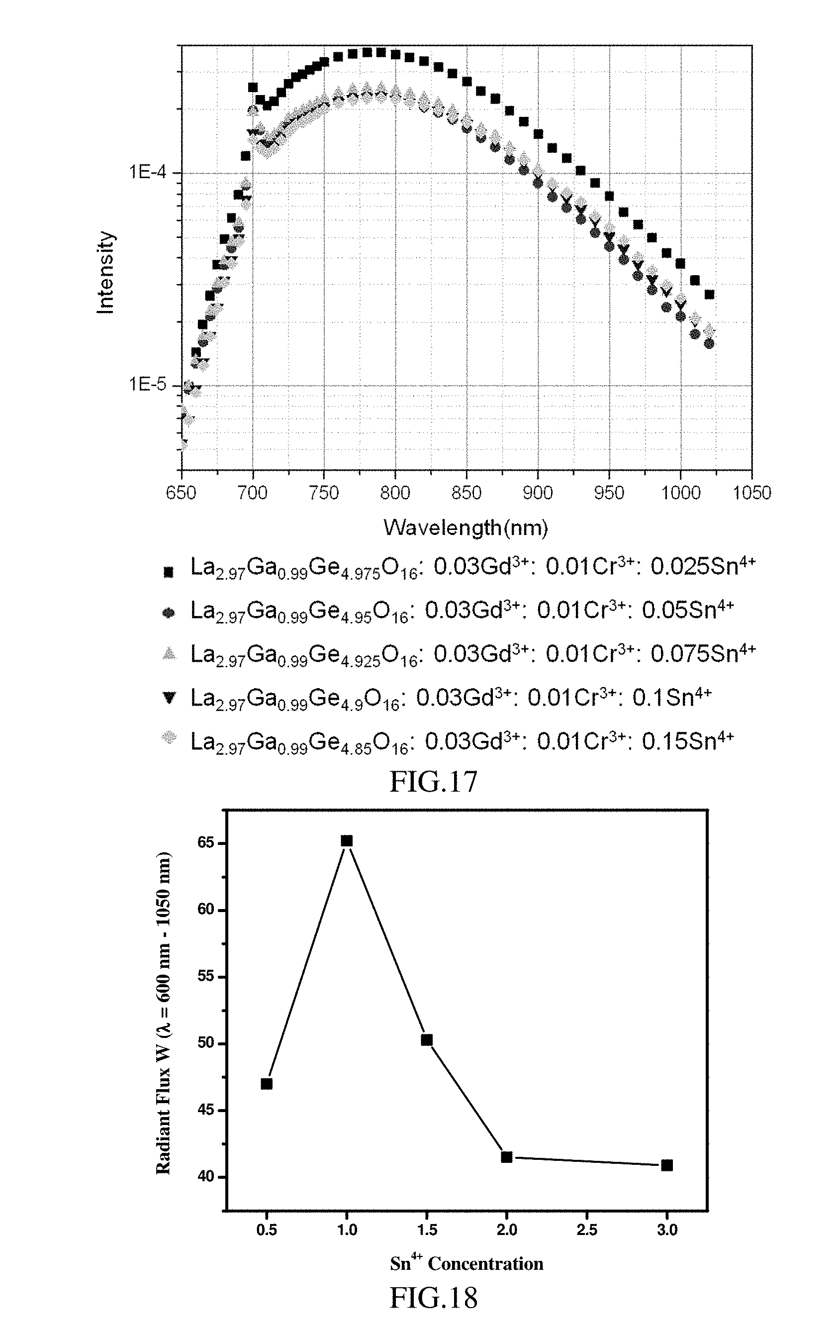
[0134] This experimental example aims to investigate the effects of different doping concentrations of Sn.sup.4+ on the radiant flux. Taking the phosphor having the general formula of La.sub.3(1-x)Ga.sub.1-yGe.sub.5(1-z)O.sub.16: 3xGd.sup.3+, yCr.sup.3+, 5zSn.sup.4+ (3x=0.03, y=0.01, 0<5z0.2) as an example, the basic parameters of the optoelectronic component used for testing are shown in Table 1; the doping concentration of Sn.sup.4+and the corresponding radiant flux are shown in Table 5; the photoluminescence emission spectrums of phosphors with different doping concentrations of Sn.sup.4+ are shown in FIG. 17; and a graph showing the relationship between the doping concentration of Sn.sup.4+ and the radiant flux (the wavelength range is 650-1050 nm) is shown in FIG. 18.
TABLE-US-00005 TABLE 5 Doping concen- Radiant flux tration - (.lamda. = Phosphor chemical formula Sn.sup.4+ 650-1050 nm) La.sub.2.97Ga.sub.0.99Ge.sub.4.975O.sub.16: 0.03Gd.sup.3+: 0.01Cr.sup.3+: 0.5% 47.0 mW 0.025Sn.sup.4+ La.sub.2.97Ga.sub.0.99Ge.sub.4.95O.sub.16: 0.03Gd.sup.3+: 0.01Cr.sup.3+: 1.0% 65.2 mW 0.05Sn.sup.4+ La.sub.2.97Ga.sub.0.99Ge.sub.4.925O.sub.16: 0.03Gd.sup.3+: 0.01Cr.sup.3+: 1.5% 50.3 mW 0.075Sn.sup.4+ La.sub.2.97Ga.sub.0.99Ge.sub.4.9O.sub.16: 0.03Gd.sup.3+: 0.01Cr.sup.3+: 2.0% 41.5 mW 0.1Sn.sup.4+ La.sub.2.97Ga.sub.0.99Ge.sub.4.85O.sub.16: 0.03Gd.sup.3+: 0.01Cr.sup.3+: 3.0% 40.9 mW 0.15Sn.sup.4+
[0135] As can be seen from Table 5 and FIG. 17-FIG. 18, in the phosphor La.sub.3(1-x)Ga.sub.1-yGe.sub.5(1-z)O.sub.16: 3xGd.sup.3+, yCr.sup.3+, 5zSn.sup.4+, when the doping concentration of Sn.sup.4+is greater than or equal to 0.5%, the radiant flux is greater than 40 mW. Moreover, as the doping concentration of Sn.sup.4+ increases, the radiant flux first increases to the peak value accordingly and then decreases. When the doping concentration of Sn.sup.4+ is about 1% (the corresponding phosphor is La.sub.2.97Ga.sub.0.99Ge.sub.4.95O.sub.16: 0.03Gd.sup.3+: 0.01Cr.sup.3+: 0.05Sn.sup.4+), the radiant flux reaches the highest of 65.2 mW.
Comparative Example 1
[0136] The present comparative example provides a phosphor having a chemical formula of La.sub.3Ga.sub.4.95GeO.sub.14: 0.05Cr.sup.3+ (the doping concentration of Cr.sup.3+ is 1%), a comparison between the radiant flux of the phosphor and that of La.sub.3Ga.sub.0.99Ge.sub.5O.sub.16: 0.01Cr.sup.3+ is shown in Table 6; FIG. 19 is the photoluminescence emission spectrum of the above two phosphors. As shown in Table 6 and with reference to FIG. 19, in both the visible range of 372-650 nm and the red visible and near-infrared range of 650-1050 nm, the radiant flux of La.sub.3Ga.sub.4.95GeO.sub.14: 0.05Cr.sup.3+ is significantly smaller than the radiant flux of La.sub.3Ga.sub.0.99Ge.sub.5O.sub.16: 0.01Cr.sup.3+, indicating that the phosphor provided in the present application is far superior to the conventional phosphors.
TABLE-US-00006 TABLE 6 Phosphor Total Radiant flux Radiant flux chemical formula radiant flux (.lamda. = 372-650 nm) (.lamda. = 650-1050 nm) La.sub.3Ga.sub.4.95GeO.sub.14: 195.6 mW 184.5 mW 10.1 mW 0.05Cr.sup.3+ La.sub.3Ga.sub.0.99Ge.sub.5O.sub.16: 344.2 mW 326.8 mW 17.6 mW 0.01Cr.sup.3+
EXAMPLE 7
[0137] The present example provides a set of phosphors having the general formula of La.sub.3Ga.sub.5(1-x)Ge.sub.1-yO.sub.14: 5xCr.sup.3+, ySn.sup.4+, where 0<x<0.1, y=0. The chemical formulae of the set of phosphors are as follows:
[0138] La.sub.3Ga.sub.4.95GeO.sub.14: 0.05Cr.sup.3+
[0139] La.sub.3Ga.sub.4.75GeO.sub.14: 0.25Cr.sup.3+
[0140] La.sub.3Ga.sub.4.55GeO.sub.14: 0.45Cr.sup.3+
[0141] The preparing method of the set of phosphor is as follows: according to stoichiometric ratios in the molecular formulae of the set of phosphors, accurately weighing the raw materials La.sub.2O.sub.3, Ga.sub.2O.sub.3, GeO.sub.2 and Cr.sub.2O.sub.3; placing the weighed raw materials in an agate mortar to grind for evenly mixing; then transferring the resulting mixture to an alumina crucible; placing in a tubular furnace and sintering in an air atmosphere; controlling the temperature at about 1300.degree. C. to sinter for about 5 hours; and after cooling in the furnace, grinding into powders to obtain the phosphor.
[0142] As shown in FIG. 20, the XRD diffraction spectrums of the set of phosphors are compared with the standard spectrum JCPDS 722464 (ICSD-20783). The diffraction peaks of the set of phosphors are consistent with the standard spectrum and no impurity peak is detected, indicating that the activator Cr.sup.3+ and the sensitizer Sn.sup.4+ successfully entered into the crystal lattice. The crystals of the set of phosphors belong to the triclinic system, and the space group is P-1(2).
[0143] As shown in FIG. 21, when excited by the excitation light of 460 nm, the emission spectrum of the set of phosphors cover a range of 600-1250 nm, especially a range of 650-1050 nm.
EXAMPLE 8
[0144] The present example provides a set of phosphors having the general formula of La.sub.3Ga.sub.5(1-x)Ge.sub.1-yO.sub.14: 5xCr.sup.3+, ySn.sup.4+, where x=0.01, 0<y0.9. The chemical formulae of the set of phosphors are as follows:
[0145] La.sub.3Ga.sub.4.95Ge.sub.0.9O.sub.14: 0.05Cr.sup.3+, 0.1Sn.sup.4+;
[0146] La.sub.3Ga.sub.4.95Ge.sub.0.7O.sub.14: 0.05Cr.sup.3+, 0.3Sn.sup.4+;
[0147] La.sub.3Ga.sub.4.95Ge.sub.0.5O.sub.14: 0.05Cr.sup.3+, 0.5Sn.sup.4+.
[0148] The preparing method of the set of phosphors is as follows: according to stoichiometric ratios in the molecular formulae of the set of phosphors, accurately weighing the raw materials La.sub.2O.sub.3, Ga.sub.2O.sub.3, GeO.sub.2, SnO.sub.2 and Cr.sub.2O.sub.3; and placing the weighed raw materials in an agate mortar to grind for evenly mixing; then transferring the resulting mixture to an alumina crucible; placing in a muffle furnace and sintering in an air atmosphere; controlling the temperature at about 1250.degree. C. to sinter for about 5 hours; and after cooling in the furnace, grinding into powders to obtain the phosphor.
[0149] As shown in FIG. 11-FIG. 24, the X-ray diffraction spectrums of the set of phosphors are compared with the standard X-ray diffraction spectrum. All the diffraction peaks of the set of phosphors are consistent with the standard spectrum JCPDS 722464 (ICSD-20783) and no impurity peak is detected, indicating that the activator Cr.sup.3+ and the sensitizer Sn.sup.4+ successfully entered into the crystal lattice. Further, the crystals of the set of phosphors belong to the triclinic system, and the space group is P-1(2).
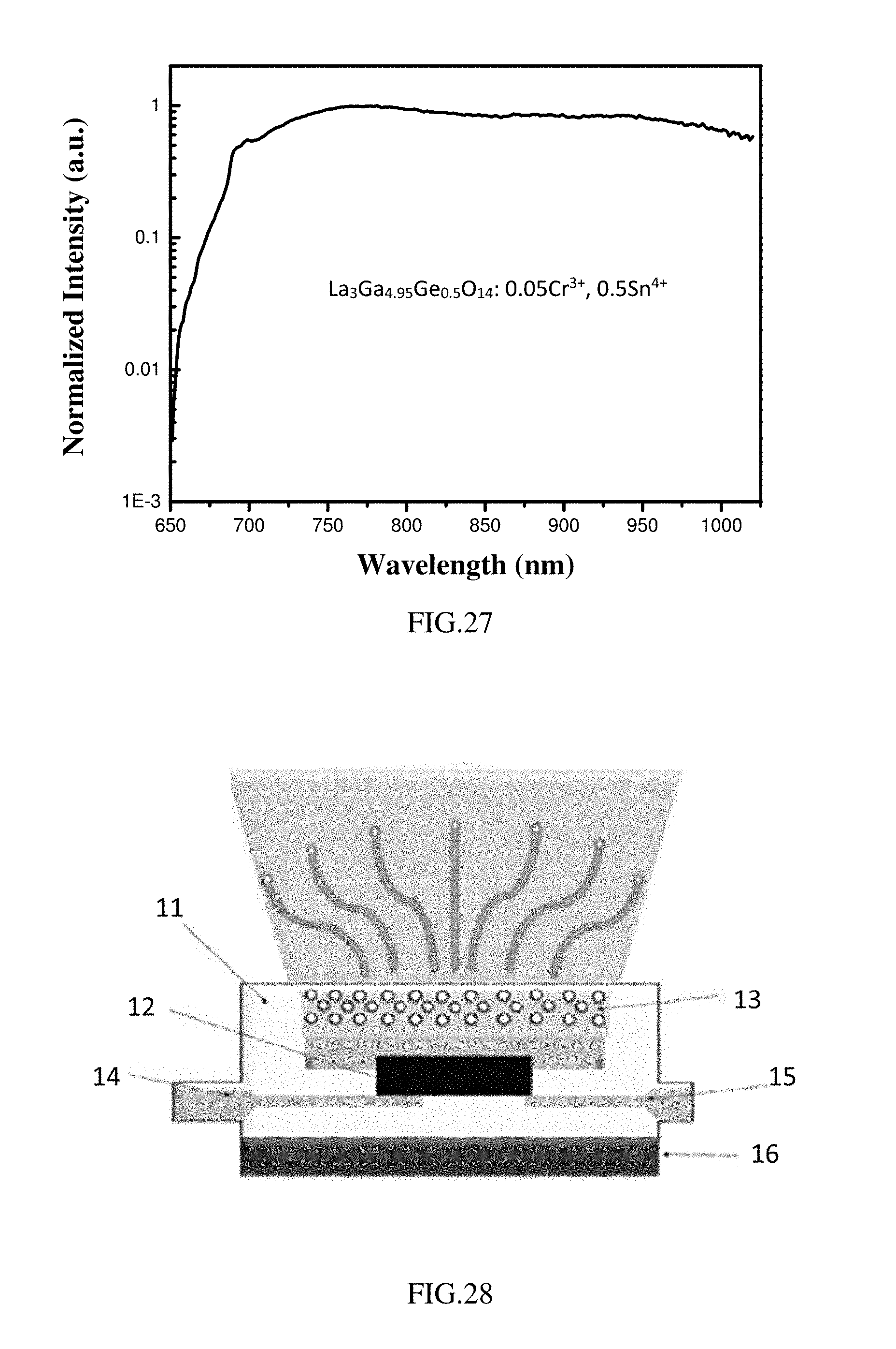
[0150] As shown in FIG. 25-FIG. 27, when excited by the excitation light of 460 nm, the emission spectrums of the set of phosphors cover a range of 600-1100 nm, especially a range of 650-1050 nm.
EXAMPLE 9
[0151] The present example provides an optoelectronic component. As shown in FIG. 28, the optoelectronic component includes a housing 11 provided with a recess 16, a semiconductor chip 12 for emitting a primary radiation, and a first lead 14 and a second lead 15 respectively connected to thea housing 11. An inner side wall of the recess 16 is coated with a suitable material to achieve a selective reflection of light; the semiconductor chip 12 is mounted in the recess 16 and is respectively connected to the first lead 14 and the second lead 15 which are opaque. a conversion unit 13 is mounted on an optical path of the primary radiation emitted from the semiconductor chip 12. The conversion unit 13 contains or is provided with the phosphor according to Example 7 described above. Specifically, the phosphor is dispersed in the epoxy resin, and the conversion unit 13 is produced and dispersed outside the semiconductor chip 12 to absorb the primary radiation emitted from the semiconductor chip 12 and converted into a secondary radiation.
[0152] The basic parameters of the above optoelectronic component are shown in Table 7; under these basic parameters, the measurement results of the radiant flux obtained when part of the phosphors provided in Example 7 is used for the conversion unit 13 are shown in Table 8. The measurement results of the radiant flux obtained when part of the phosphors provided in Example 8 is used for the conversion unit 13 are shown in Table 9.
TABLE-US-00007 TABLE 7 LED Phosphor packaging Silicone content in the bracket LED chip specifications encapsulant conversion unit PPA3535 Size: 40 mil * 40 mil 1.4 Silicone 50 wt % Luminescence wavelength: 450-452.5 nm Power: 109.7 mW
TABLE-US-00008 TABLE 8 Doping concentration - Radiant flux Phosphor chemical formula Cr.sup.3+ (.lamda. = 650-1050 nm) La.sub.3Ga.sub.4.95GeO.sub.14: 0.05Cr.sup.3+ 1% 10.5 mW La.sub.3Ga.sub.4.75GeO.sub.14: 0.25Cr.sup.3+ 5% 7.8 mW La.sub.3Ga.sub.4.55GeO.sub.14: 0.45Cr.sup.3+ 9% 4.7 mW
[0153] As shown in Table 8, as the doping concentration of Cr.sup.3+ is gradually increased, the radiant flux is correspondingly decreased, but when the doping concentration of Cr.sup.3+ is 9%, the radiant flux corresponding to the phosphor is still greater than 4 mW.
TABLE-US-00009 TABLE 9 Total Phosphor chemical radiant Radiant flux Radiant flux formula flux (.lamda. = 372-650 nm) (.lamda. = 650-1050 nm) La.sub.3Ga.sub.4.95Ge.sub.0.9O.sub.14: 150.6 mW 135.8 mW 14.8 mW 0.05Cr.sup.3+, 0.1Sn.sup.4+ La.sub.3Ga.sub.4.95Ge.sub.0.7O.sub.14: 125.3 mW 111.5 mW 13.8 mW 0.05Cr.sup.3+, 0.3Sn.sup.4+ La.sub.3Ga.sub.4.95Ge.sub.0.5O.sub.14: 157.9 mW 143.6 mW 14.3 mW 0.05Cr.sup.3+, 0.5Sn.sup.4+
[0154] Finally, it should be noted that the above examples are only used to illustrate the technical solutions of the present application, rather than limiting the present application; a person skilled in the art may still modify the technical solutions described in the foregoing examples, or make equivalent replacements to some or all of the technical features therein. However, these modifications or replacements do not make the essence of corresponding technical solutions depart from the scope of the technical solutions in the examples of the present application, but should fall into the scope of the claims and specification of the present application.
* * * * *
D00000
D00001
D00002
D00003
D00004
D00005
D00006
D00007
D00008
D00009
D00010
D00011
D00012

D00013

D00014

D00015
P00001

XML
uspto.report is an independent third-party trademark research tool that is not affiliated, endorsed, or sponsored by the United States Patent and Trademark Office (USPTO) or any other governmental organization. The information provided by uspto.report is based on publicly available data at the time of writing and is intended for informational purposes only.
While we strive to provide accurate and up-to-date information, we do not guarantee the accuracy, completeness, reliability, or suitability of the information displayed on this site. The use of this site is at your own risk. Any reliance you place on such information is therefore strictly at your own risk.
All official trademark data, including owner information, should be verified by visiting the official USPTO website at www.uspto.gov. This site is not intended to replace professional legal advice and should not be used as a substitute for consulting with a legal professional who is knowledgeable about trademark law.