Selection Control for Transformer Winding Input in a Power Converter
Lind; Anders ; et al.
U.S. patent application number 15/827194 was filed with the patent office on 2019-05-30 for selection control for transformer winding input in a power converter. The applicant listed for this patent is Infineon Technologies Austria AG. Invention is credited to Anders Lind, Andrey Malinin.
| Application Number | 20190165685 15/827194 |
| Document ID | / |
| Family ID | 66633667 |
| Filed Date | 2019-05-30 |


| United States Patent Application | 20190165685 |
| Kind Code | A1 |
| Lind; Anders ; et al. | May 30, 2019 |
Selection Control for Transformer Winding Input in a Power Converter
Abstract
Circuits and methods are provided for supplying power to a transformer of a switching DC/DC voltage converter within a power converter. The power converter includes separate nodes that can potentially supply such power. A first of these nodes is coupled, typically directly and with no energy-storing bulk capacitor, to a rectifier that supplies rectified power from an alternating current power source. A second node is also supplied power from the rectifier, but is coupled to a bulk capacitor that can store and supply energy as needed. The techniques disclosed herein use the first node to supply power to the transformer when feasible, and use the second node, and its associated bulk capacitor, to supply power otherwise. In so doing, the energy storage requirements of the bulk capacitor may be reduced, meaning that the capacitance and associated size of the bulk capacitor may be reduced relative to other power converter circuits.
| Inventors: | Lind; Anders; (San Jose, CA) ; Malinin; Andrey; (Fort Collins, CO) | ||||||||||
| Applicant: |
|
||||||||||
|---|---|---|---|---|---|---|---|---|---|---|---|
| Family ID: | 66633667 | ||||||||||
| Appl. No.: | 15/827194 | ||||||||||
| Filed: | November 30, 2017 |
| Current U.S. Class: | 1/1 |
| Current CPC Class: | H02M 3/33523 20130101; H02M 2001/0032 20130101; H02M 1/4258 20130101; H02M 1/08 20130101; H02M 1/4266 20130101; H02M 3/33569 20130101; H02M 1/143 20130101 |
| International Class: | H02M 3/335 20060101 H02M003/335; H02M 1/08 20060101 H02M001/08; H02M 1/14 20060101 H02M001/14 |
Claims
1. A power converter, comprising: a rectifier configured to input alternating current (AC) power from an input power source and supply power to a rectified voltage node having a rectified voltage; a bulk capacitor that is supplied power from the input power source and has a storage voltage; a transformer comprising a primary-side winding; a first switch configured to provide power to the primary-side winding from the rectified voltage node; a second switch configured to provide power to the primary-side winding from the bulk capacitor; and a controller configured to: sense at least one of the rectified voltage and the storage voltage, responsive to detecting that the rectified voltage is decreasing over time and is above a first threshold, switch the first switch while holding the second switch off, responsive to detecting that rectified voltage is below the first threshold and is greater than the storage voltage, switch the first switch to provide power to the primary-side winding from the rectified voltage node, and responsive to detecting that the rectified voltage is below the first threshold and is lower than the storage voltage, switch the second switch to provide power to the primary-side winding from the bulk capacitor.
2-3. (canceled)
4. The power converter of claim 1, wherein the controller is further configured to: responsive to detecting that the rectified voltage is increasing over time and that the rectified voltage is greater than a threshold, switch both the first switch and the second switch until it is detected that the rectified voltage is no longer increasing over time.
5. The power converter of claim 1, wherein the controller is further configured to operate in a low-power mode, such that power is supplied to the primary winding from the bulk capacitor for several cycles of the input power source by turning the first switch off and by switching the second switch such that power pulses are supplied to the primary-side winding at no more often than once per cycle of the input power source.
6. The power converter of claim 1, further comprising: a current-blocking device coupled to the bulk capacitor and configured to supply power to the bulk capacitor, the current-blocking device additionally coupled to the rectified voltage node or the input power source.
7. The power converter of claim 6, wherein the current-blocking device is a bi-directional switch capable of blocking current flow in both directions.
8. The power converter of claim 7, wherein the bi-directional switch is comprised of two transistors configured in series.
9. The power converter of claim 6, wherein the controller is further configured to control the current-blocking device based upon a measurement of the rectified voltage or a voltage of the input power source, so as to only allow current to be conducted to the bulk capacitor in response to detecting that the measured rectified voltage or measured input power source voltage is below a maximum allowed voltage of the bulk capacitor, and so as to not allow current to be conducted from the bulk capacitor to the rectified voltage node or input power source.
10. The power converter of claim 7, wherein the controller is further configured to operate in a low-power mode, such that power is supplied to the primary winding from the bulk capacitor for several cycles of the input power source by turning the first switch off and by switching the second switch such that energy pulses are supplied to the primary winding at no more often than once per cycle of the input power source, and wherein the bi-directional switch is controlled to ensure the source voltage is below a low-power source voltage threshold, by measuring the rectified voltage or a voltage of the input power source, and turning the bi-directional switch on responsive to detecting that the measured voltage is within a low-power voltage range.
11. (canceled)
12. The power converter of claim 1, wherein the power converter has an output power rating in Watts, and wherein the bulk capacitor has a capacitance of 1.0 to 1.4 .mu.F per Watt of the output power rating.
13. A method of controlling a power converter that includes a rectifier configured to input alternating current (AC) power from an input power source and supply power to a rectified voltage node having a rectified voltage node, a bulk capacitor that is supplied power from the input power source and has a storage voltage, a transformer comprising a primary-side winding, a first switch configured to provide power to the primary-side winding from the rectified voltage node, and a second switch configured to provide power to the primary-side winding from the bulk capacitor, the method comprising: sensing at least one of the rectified voltage and the storage voltage; responsive to detecting that the rectified voltage is decreasing over time and is above a first threshold, switching the first switch while holding the second switch off; responsive to detecting that the rectified voltage is below the first threshold and is greater than the storage voltage, switching the first switch to provide power to the primary-side winding from the rectified voltage node, and responsive to detecting that the rectified voltage is below the first threshold and is lower than the storage voltage, switching the second switch to provide power to the primary-side winding from the bulk capacitor.
14-15. (canceled)
16. The method of claim 13, further comprising: responsive to detecting that the rectified voltage is increasing over time and that the rectified voltage is greater than a threshold, switching both the first switch and the second switch until it is detected that the rectified voltage is no longer increasing over time.
17. The method of claim 13, further comprising: detecting that a load of the power converter requires power below a low-power threshold, and entering a low-power mode of the power converter; switching, for a plurality of cycles of the input power source during the low-power mode, the second switch such that power pulses are supplied to the primary-side winding at a rate no more often than once per cycle of the input power source, so as to supply power to the primary-side winding from the bulk capacitor; and turning off the first switch for the plurality of cycles of the input power source.
18. The method of claim 13, wherein the power converter further comprises a bi-directional switch configured to block current flow in both directions and configured to supply power to the bulk capacitor from at least one of the rectified voltage node and the input power source, the method further comprising: sensing at least one of the rectified voltage and a voltage of the input power source; detecting that the measured rectified voltage or the measured input power source voltage is above a maximum allowed voltage of the bulk capacitor; responsive to said detecting, holding the bi-directional switch in the off position such that it does not conduct, so as to prevent the storage voltage of the bulk capacitor from being above the maximum allowed voltage.
19. The method of claim 13, wherein the power converter further comprises a bi-directional switch configured to block current flow in both directions and configured to supply power to the bulk capacitor from a capacitor source that is at least one of the rectified voltage node and the input power source, the method further comprising: detecting that a load of the power converter requires power below a low-power threshold, and entering a low-power mode of the power converter; and during the low-power mode: turning the first switch off such that it does not conduct; switching the second switch such that energy pulses are supplied to the primary-side winding at a rate no more often than once per cycle of the input power source; measuring a voltage of the capacitor source; and turning on the bi-directional switch responsive to detecting that the voltage of the capacitor source is within a low-power source voltage range, thereby charging the bulk capacitor.
20. (canceled)
Description
TECHNICAL FIELD
[0001] The present application relates to power converters and, in particular, relates to circuits comprising a first rectified voltage node having no bulk capacitor and a second rectified voltage node coupled to a bulk capacitor, and to controlling a selection of whether the first rectified voltage node or the second rectified voltage node or both are used for supplying power to a transformer.
BACKGROUND
[0002] Line power converters input alternating current (AC) power and convert it into direct current (DC) power for supplying a load, e.g., charging batteries in smart phones, laptops, or other portable devices, or for otherwise powering an electronic device. Such power converters typically include an input stage, which converts an input AC voltage into an intermediate voltage that is DC, and a switching DC/DC converter, which converts the intermediate DC voltage into an output DC voltage level that is appropriate for powering the load.
[0003] Power converters limited to low or moderate power requirements, e.g., below an input power of 75 W, typically require no power factor correction. The input stage for such power converters typically includes a protection circuit, an electromagnetic interference (EMI) filter, a bridge rectifier, and a bulk capacitor. The EMI filter and the protection circuit are connected to an input power source, such as an AC line voltage provided by an electrical mains. The output of the protection circuit and the EMI filter is provided to a rectifier, such as a diode-based bridge rectifier, that outputs a rectified voltage. The rectified voltage is coupled to the bulk capacitor, which stores energy and smoothes the rectified (DC) voltage. More particularly, this smoothed voltage may be characterized as having an average (DC) value with a ripple superimposed on it, wherein the ripple frequency is related to a frequency of the AC power source (e.g., 50 Hz, 60 Hz) and the ripple magnitude is largely determined by the value of the bulk capacitor.
[0004] The intermediate DC voltage is input to the switching DC/DC voltage converter. The DC/DC voltage converter includes a transformer comprised of primary and secondary windings. One or more power switches switchably couple the intermediate DC voltage onto the primary winding(s) of the DC/DC voltage converter, thereby producing an AC voltage across the primary winding(s). This induces an AC voltage on the secondary winding(s) of the DC/DC voltage converter. The secondary-side voltage and current are rectified and filtered before being provided to the power converter load. The DC/DC voltage converter operates optimally when its input intermediate DC voltage is constant. In practice, the bulk capacitance is chosen so as to constrain the ripple of the intermediate DC voltage to be within an acceptably narrow range. The DC/DC voltage converter may specify an acceptable voltage range for this input, or may specify a minimum allowed input voltage.
[0005] Power converters configured to work with various AC mains voltage levels, i.e., universal input converters, require a bulk capacitor capable of handling fairly large voltages. For example, a capacitor voltage rating of 400V may be necessary to handle line voltages of 340V peak (240 V.sub.RMS), as used in much of the world, together with some margin for lightning surges, etc. The bulk capacitor must also have a fairly large capacitance so as to meet the input voltage requirements (voltage ripple and/or minimum voltage) of the DC/DC voltage converter. For example, a capacitance of 1.5 to 2.0 .mu.F per Watt of power rating for the power converter may be required.
[0006] The physical size (volume and printed circuit board footprint) of the bulk capacitor within a typical power converter is quite large due to its required capacitance and maximum voltage ratings. The size requirements for DC/DC voltage converters are on a gradual downward trajectory, as their constituent components, e.g., transformer, capacitors, inductors, may be reduced in size as the switching frequency of DC/DC voltage converters increases. However, such scaling does not apply to the bulk capacitor, as the input voltage frequency is fixed to that provided by the power source, e.g., the mains voltage. The bulk capacitor already consumes a large portion of the overall volume for a power converter, and this portion is increasing due to the gradually decreasing size requirements for the DC/DC voltage converter.
[0007] One technique for reducing the capacitance of the bulk capacitor is to include a non-isolated boost converter that pre-regulates the input voltage to a much higher voltage (e.g., 400V) that is fed to the DC/DC voltage converter. This is the approach taken by power factor correction (PFC) converters. Because a much higher voltage is provided to the DC/DC voltage converter, a smaller bulk capacitor may be used while still meeting minimum voltage input requirements of the DC/DC voltage converter. However, such an approach has drawbacks in terms of efficiency, as the added conversion stage has associated power loss. Furthermore, the boost converter employs a fairly large input inductor, which largely negates any size reduction of the bulk capacitor. Hence, the complexity and size of an added input stage, e.g., a boost or other PFC converter, makes such approaches undesirable, at least for lower-power converters that do not require PFC.
[0008] Circuits and associated techniques are desired that would allow for a reduction in the bulk capacitor used within power converters.
SUMMARY
[0009] According to an embodiment of a power converter, the power converter includes a rectifier, a bulk capacitor, a transformer having a primary-side winding, first and second switches, and a controller. The rectifier is configured to input alternating current (AC) power from an input power source and to supply power to a rectified voltage node having a rectified voltage. The bulk capacitor is supplied power from the input power source, e.g., via the rectified voltage node or directly from the input power source via diodes, and has an associated storage voltage. The first and second switches are configured to supply power to the primary-side winding. The first switch supplies power from the rectified voltage node, whereas the second switch supplies power from the bulk capacitor. The controller provides control signals to the first and second switches so as to control the power provided to the primary-side windings. The controller determines whether to switch the first switch, the second switch, or both switches based upon at least one of the rectified voltage and the storage voltage.
[0010] According to an embodiment of a method, the method provides techniques for controlling a power converter that comprises a rectifier configured to input alternating current (AC) power from an input power source and supply power to a rectified voltage node having a rectified voltage node, a bulk capacitor that is supplied power from the input power source and has a storage voltage, a transformer comprising a primary-side winding, a first switch configured to provide power to the primary-side winding from the rectified voltage node, and a second switch configured to provide power to the primary-side winding from the bulk capacitor. The method begins by sensing at least one of the rectified voltage and the storage voltage. Next, it is determined whether the first switch, the second switch, or both switches will be switched, based upon the sensed rectified voltage and/or the sensed storage voltage. Control signals are generated and provided to the determined switches so as to provide power to the primary-side winding.
[0011] Those skilled in the art will recognize additional features and advantages upon reading the following detailed description, and upon viewing the accompanying drawings.
BRIEF DESCRIPTION OF THE FIGURES
[0012] The elements of the drawings are not necessarily to scale relative to each other. Like reference numerals designate corresponding similar parts. The features of the various illustrated embodiments may be combined unless they exclude each other. Embodiments are depicted in the drawings and are detailed in the description that follows.
[0013] FIG. 1 illustrates a schematic diagram of a power converter having a primary-side winding that is supplied power from one or both of two different voltage nodes.
[0014] FIG. 2 illustrates a controller for a power converter such as the power converter of FIG. 1.
[0015] FIG. 3A illustrates voltage waveforms corresponding to two different nodes such as those included in the power converter of FIG. 1.
[0016] FIG. 3B illustrates voltage waveforms corresponding to nodes within a power converter in which power is supplied to a primary-side winding only from a bulk capacitor.
[0017] FIG. 4 illustrates an alternative power converter that includes a second rectifier and a filter capacitor.
[0018] FIG. 5 illustrates another alternative power converter in which power to the primary-side winding is switched on the ground side of the winding.
[0019] FIG. 6 illustrates a power converter in which power is supplied to a bulk capacitor using a bi-directional switch.
[0020] FIG. 7 illustrates voltage waveforms corresponding to nodes such as the nodes included in the power converter of FIG. 6.
[0021] FIG. 8 illustrates a power converter that includes a plurality of bulk capacitors, together with associated diodes and switches.
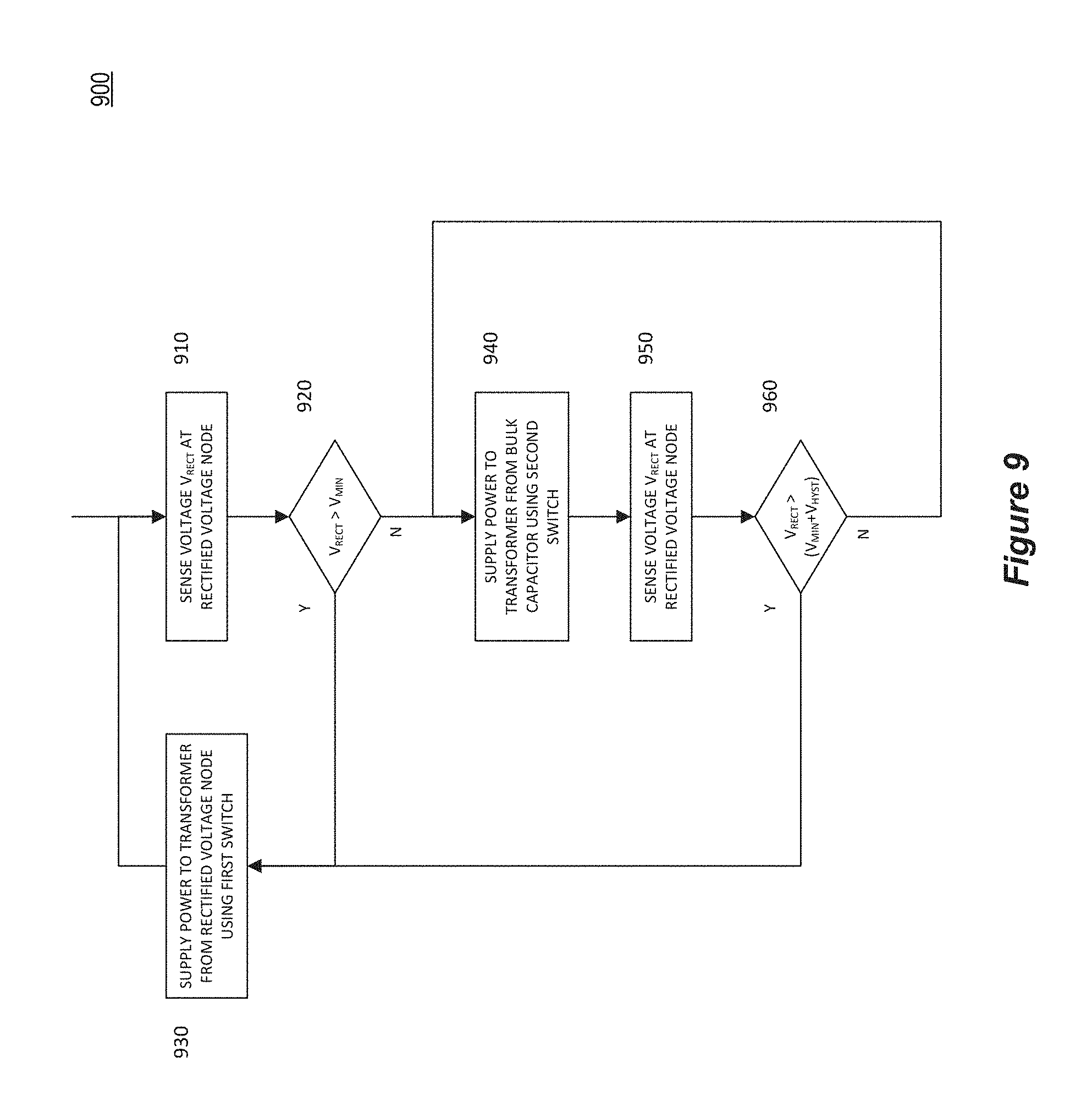
[0022] FIG. 9 illustrates a method, within a power converter, for switching power switches so as to supply power to primary-side winding(s) of a transformer from two different voltage nodes.
DETAILED DESCRIPTION
[0023] The embodiments described herein provide circuits and methods that enable a reduction in size for a bulk capacitor within a power converter that is comprised of an input stage and a switching DC/DC voltage converter. This size reduction is realized by decreasing the required capacitance and/or voltage rating of the bulk capacitor, while still meeting input voltage requirements for the switching DC/DC voltage converter. Described below are circuit topologies, together with techniques for controlling such circuit topologies, that enable such a reduction in capacitance and/or voltage rating. Unlike conventional power converters that couple a rectifier output to a bulk capacitor and to a power stage input of a switching DC/DC voltage converter, the circuits described herein include both a first rectified voltage node, which cannot be powered from the bulk capacitor, and a second rectified voltage node, which is coupled to and can be powered from the bulk capacitor. Voltages corresponding to one or both of the first and second rectified voltage nodes are measured and used to determine whether power from the first rectified voltage node, the second rectified voltage node, or both should be provided to the transformer of the switching DC/DC voltage converter.
[0024] The switching DC/DC voltage converter includes a transformer having primary and secondary-side windings. A first power switch is configured to switchably couple the first rectified voltage node to the primary-side winding. A second power switch is configured to switchably couple the second rectified voltage node to the primary-side winding. A controller determines whether the first power switch, and its associated first rectified voltage node, or the second power switch, and its associated second rectified voltage node, or both should supply power to the primary-side winding. Such determination is based upon a voltage measured at the first rectified voltage node and/or a voltage measured at the second rectified voltage node. In a preferred embodiment, the first power switch and the first rectified voltage node are selected to power the primary-side winding when the measured voltage of the first rectified voltage node is above a minimum voltage threshold. Otherwise, the controller determines which of the first and second voltage nodes has a higher measured voltage, and selects the associated power switch to provide power to the primary-side winding. In a typical case, when the measured voltage at the rectified voltage node is below the minimum voltage threshold, the controller will switch the second switch thereby supplying power to the primary-side winding from the energy stored in the bulk capacitor. Once this determination is made, the controller switches the selected power switch in order to meet the power requirements for a load of the power converter.
[0025] The inventive techniques may be applied to a variety of power converters that rely upon switched DC/DC voltage conversion. For ease of explanation, the inventions are described by way of particular examples in the context of a flyback converter. One skilled in the art will recognize that the techniques are readily extrapolated to other power converter topologies, such as forward converters, and other variants, such as quasi-resonant (QR) converters and active clamp converters. The controller in the examples described below is located on the primary side of the controller, but the controller could be located on the secondary side. This would require modifications such as isolation circuits, as are known in the art. Furthermore, the described circuits include a transformer having a primary and a secondary-side winding. The control techniques described herein may also be applied to other transformer configurations including, e.g., transformers including multiple primary-side windings, multiple secondary-side windings, and/or one or more auxiliary windings.
[0026] It should be understood that the particular examples described below are not meant to be limiting. Circuits and techniques that are well-known in the art are not described in detail, so as to avoid obscuring the unique aspects of the invention. Features and aspects from the example embodiments may be combined or re-arranged, except where the context does not allow this.
Power Converter with Separate Voltage Nodes to Power Primary-Side Winding
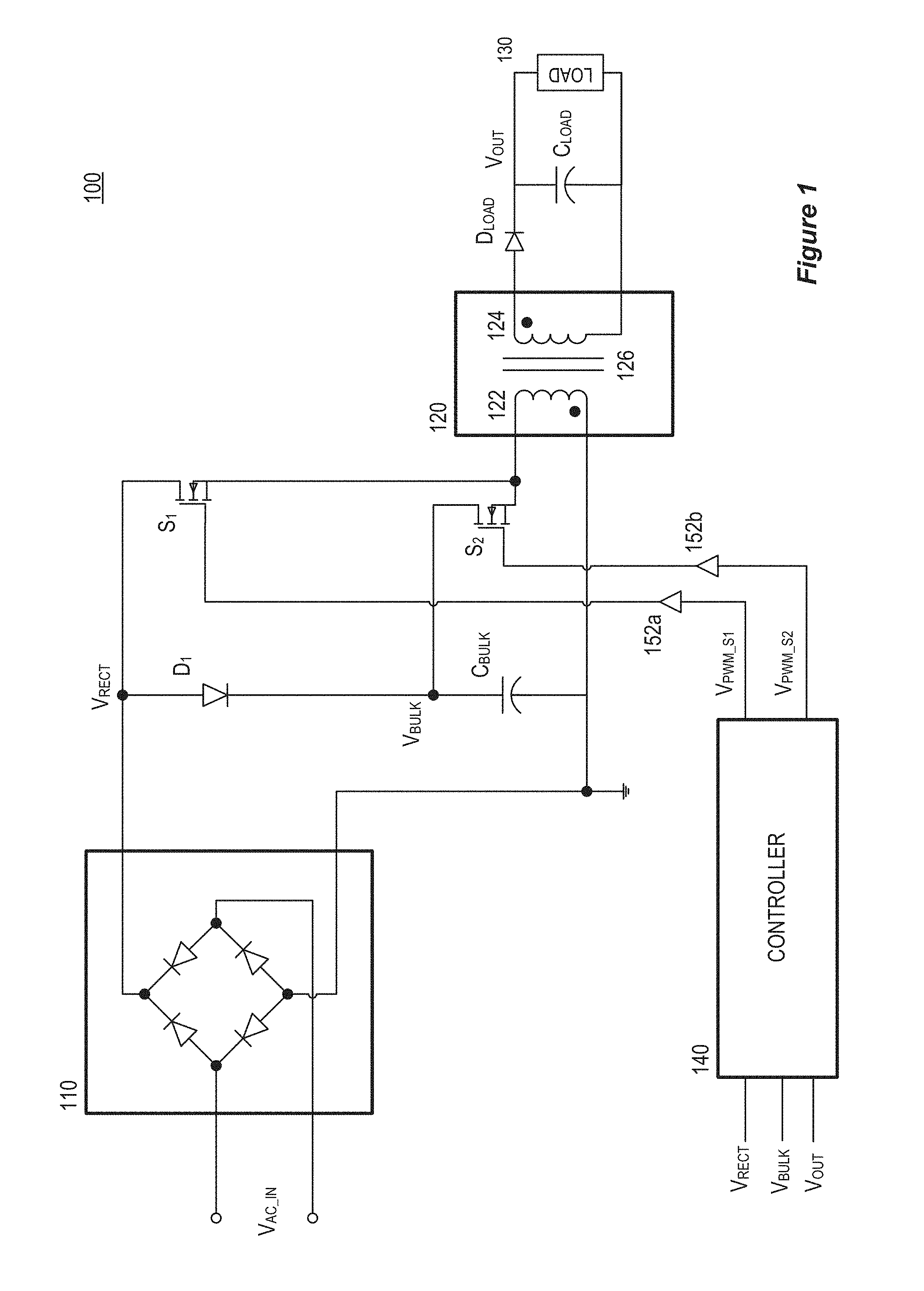
[0027] FIG. 1 illustrates an embodiment of a forward power converter 100. This power converter 100 differs from conventional power converters in that it includes a first rectified voltage node, denoted V.sub.RECT, and a second rectified voltage node, denoted V.sub.BULK. The first rectified voltage node V.sub.RECT is coupled directly to a bridge rectifier 110, and is not coupled to an energy-storage component, such as a bulk capacitor, that is capable of supplying substantial energy to the first rectified voltage node. (A filter capacitor, having a relatively small capacitance and having a primary function of reducing high-frequency noise, is not considered a bulk capacitor in this context.) The second rectified voltage node V.sub.BULK is also supplied power from the bridge rectifier 110, but is coupled to a bulk capacitor C.sub.BULK which serves as an energy-storage component. A controller 140 determines which of the rectified voltage nodes V.sub.RECT, V.sub.BULK should be coupled to the primary side of a transformer 120 when the DC/DC voltage converter is switched. By using the first rectified voltage node V.sub.RECT whenever it is capable of meeting minimum voltage requirements for the switching DC/DC voltage converter, the power converter 100 is less reliant on the second rectified voltage node V.sub.BULK and the energy stored in the bulk capacitor C.sub.BULK. This, in turn, means that the capacitance and associated size of the bulk capacitor C.sub.BULK may be reduced relative to power converters that do not include or use a first rectified voltage node such as the node V.sub.RECT within FIG. 1. With these unique features of the power converter 100 summarized above, the power converter 100 of FIG. 1 will now be described in further detail.
[0028] The power converter 100 includes a bridge rectifier 110, a transformer 120, power switches S.sub.1 and S.sub.2, and a controller 140. The power converter 100 supplies power to a load 130 on the secondary side of the transformer 120.
[0029] The rectifier 110 inputs power from an AC power source, denoted V.sub.AC.sub._.sub.IN, such as a mains supply. The illustrated rectifier 110 is arranged as a conventional diode bridge, though other arrangements are possible, such as active rectification based upon power switches rather than diodes. The rectifier 110 outputs a rectified voltage at a first rectified voltage node V.sub.RECT. The first rectified voltage node V.sub.RECT is coupled to a diode D.sub.1 which, in turn, is coupled to the bulk capacitor C.sub.BULK at a second rectified voltage node, denoted V.sub.BULK. The diode D.sub.1 allows current (power) to flow from the bridge rectifier 110 and the first rectified voltage node V.sub.RECT to the bulk capacitor C.sub.BULK and its voltage node V.sub.BULK, but does not allow energy to be drained from the bulk capacitor C.sub.BULK back to the first rectified voltage node V.sub.RECT. In this way, the diode D.sub.1 charges the bulk capacitor C.sub.BULK whenever the voltage at the first rectified voltage node V.sub.RECT is sufficiently higher than the voltage at the second rectified voltage node V.sub.BULK.
[0030] The transformer 120 includes a primary-side winding 122, a secondary-side winding 124, and a core 126. The first rectified voltage node V.sub.RECT is switchably coupled to the primary-side winding 122 via a first power switch S.sub.1, whereas the second rectified voltage node V.sub.BULK (is switchably coupled to the primary-side winding 122 via a second power switch S.sub.2. Current flow through the primary-side winding 122 is controlled by the first power switch S.sub.1 and/or the second power switch S.sub.2. For this embodiment, the control, e.g., switching duty cycle or frequency, of each of the power switches S.sub.1, S.sub.2 may use conventional techniques, but novel techniques are used to select which of the power switches S.sub.1, S.sub.2 should be actively used and, related, which of the voltage nodes V.sub.RECT, V.sub.BULK should provide power to the transformer 120. Such selection techniques are detailed in the descriptions of the controller 240 and its variants, which are found further below.
[0031] The power switches S.sub.1, S.sub.2 illustrated in FIG. 1 are enhancement-mode metal-oxide semiconductor field-effect transistors (MOSFETs), but other switch types may be used. For example, junction field-effect transistors (JFETs), bipolar junction transistors (BJTs), insulated gate bipolar transistors (IGBTs), high electron mobility transistors (HEMTs), or other types of power transistors may be preferred in some applications. The power switches S.sub.1, S.sub.2 may be integrated on the same semiconductor die, may each be provided on separate dies, or may otherwise be spread across a plurality of semiconductor dies. Drivers 152a, 152b provide control signals to the control terminals, e.g., MOSFET gates, of the power switches S.sub.1, S.sub.2.
[0032] Power flow through the primary-side winding 122 is magnetically coupled to the secondary-side winding 124 via the transformer core 126. A voltage induced across the secondary-side winding 124 is rectified by a diode D.sub.LOAD and filtered by a load capacitor C.sub.LOAD. The resultant voltage V.sub.OUT is provided to the load 130 of the power converter 100.
[0033] The controller 140 is responsible for controlling the power converter 100 so as to supply the necessary power (voltage V.sub.OUT and current) to the load 130. This includes generating pulse-width-modulated (PWM) signals V.sub.PWM.sub._.sub.S1, V.sub.PWM.sub._.sub.S2 that control the power switches S.sub.1, S.sub.2 via the drivers 152a, 152b. Conventional control techniques are used to generate each of these PWM waveforms, based upon load requirements. The controller senses the output voltage V.sub.OUT, the rectified voltage V.sub.RECT, and a storage voltage V.sub.BULK of the bulk capacitor. The controller 140 selects which of the PWM signals V.sub.PWM.sub._.sub.S1, V.sub.PWM.sub._.sub.2 to generate based upon these sensed voltages.
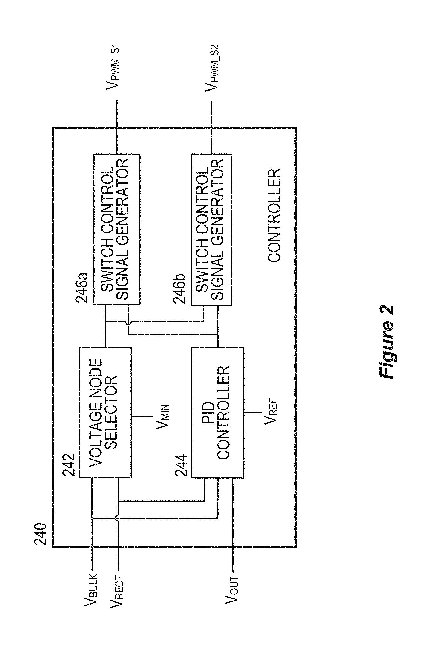
[0034] FIG. 2 illustrates an embodiment of a controller 240 for generating PWM signals V.sub.PWM.sub._.sub.S1, V.sub.PWM.sub._.sub.S2. The controller 240 includes switch control signal generators 246a, 246b that may generate PWM signals using a fixed switching frequency and a variable duty cycle. The duty cycle varies to adjust the power transfer across the transformer 120 to match the power needs of the load 130. This may be accomplished, e.g., using a proportional-integral-derivative (PID) controller 244. The PID controller 244 inputs a measured (sensed) voltage corresponding to the load voltage V.sub.OUT, and varies the duty cycle(s) to maintain the load voltage V.sub.OUT as close as feasible to a desired reference voltage V.sub.REF. Additionally, the PID controller 244 may adjust the duty cycle(s) based upon the voltage, e.g., V.sub.RECT, V.sub.BULK, that is being provided to the primary-side winding. For example, the duty cycle for a particular switching cycle may need to be increased if the provided voltage has decreased relative to a previous switch cycle. Conversely, the duty cycle may need to be reduced if the provided voltage is higher than that of a previous switching cycle. The PID controller 244 provides the duty cycle(s) to the switch control signal generators 246a, 246b, which use the duty cycle(s) to generate the PWM signals V.sub.PWM.sub._.sub.S1, V.sub.PWM.sub._.sub.S2. Operation of PID controllers for generating duty cycles for power converter switches, including techniques for making adjustments based upon an input voltage, are well-known in the art and will not be further detailed herein.
[0035] Other techniques may be used for controlling the power switches S.sub.1, S.sub.2. For example, PWM waveforms using a variable frequency and a fixed duty cycle may be used. Other power converter topologies, e.g., half-bridge, full-bridge, push-pull, may require additional power switches and associated control relative to the flyback power converter 100 illustrated within FIG. 1. While the controller 140 is illustrated as being on the primary side of the power converter 100, a similar power converter could locate a similar controller on the secondary side. Switch control techniques for other power converter topologies are well-known and will not be further explained herein, other than to note that the unique inventive techniques described within a voltage node selector 242 may be similarly applied to other power converter topologies.
[0036] The controller 240 also includes the voltage node selector 242, which is configured to read sensed voltages corresponding to one or both of the nodes V.sub.RECT, V.sub.BULK. A minimum voltage, denoted V.sub.MIN, that is required to adequately power the primary-side winding 122 is stored within a memory of the controller 240. The voltage node selector 242 monitors the measured voltage at the first rectified voltage node V.sub.RECT and compares it against the minimum voltage V.sub.MIN. When this measured voltage at V.sub.RECT is above the minimum voltage V.sub.MIN, the voltage node selector 242 selects the first rectified voltage node V.sub.RECT for powering the transformer 120. In a first sub-embodiment, when the voltage node selector 242 detects that the voltage at the first rectified voltage node V.sub.RECT has decreased to the minimum voltage V.sub.MIN, the voltage node selector 242 instead selects the second rectified voltage node V.sub.BULK, which is tied to the bulk capacitor C.sub.BULK, for powering the transformer 120.
[0037] The voltage node selector 242 selects the first rectified voltage node V.sub.RECT by enabling the first switch control signal generator 246a. The first switch control generator 246a, in turn, generates a first PWM signal V.sub.PWM.sub._.sub.S1 based upon an output of the PID controller 244, e.g., a duty cycle. The first PWM signal V.sub.PWM.sub._.sub.S1 switches the first power switch S.sub.1, via the first driver 152a, so as to generate an AC voltage across the primary-side winding 122. Power is effectively routed from the first rectified voltage node V.sub.RECT to the transformer 120. During this time interval, the second switch control signal generator 246b may be disabled, so that the second power switch S.sub.2 is left open and no power is transferred from the voltage node V.sub.BULK of the bulk capacitor C.sub.BULK.
[0038] Conversely, the voltage node selector 242 selects the second rectified voltage node V.sub.BULK, which may draw energy from the storage provided by the bulk capacitor C.sub.BULK, by enabling the second switch control signal generator 246b. The second switch control signal generator 246b generates a second PWM signal V.sub.PWM.sub._.sub.S2 in the same manner as described above, except that the voltage node V.sub.BULK provides power to the primary-side winding 122 of the transformer 120.
[0039] Regardless of which power switch S.sub.1, S.sub.2 is used and which voltage node V.sub.RECT, V.sub.BULK supplies power to the primary side of the transformer 120, the power transferred to the secondary-side winding 124 and the load 130 is similar.
[0040] The controllers 140, 240 and their constituent parts may be implemented using a combination of analog hardware components (such as transistors, amplifiers, diodes, and resistors), and processor circuitry that includes primarily digital components. The processor circuitry may include one or more of a digital signal processor (DSP), a general-purpose processor, and an application-specific integrated circuit (ASIC). The controllers 140, 240 may also include memory, e.g., non-volatile memory such as flash, that includes instructions or data for use by the processor circuitry, and one or more timers. Such memory may store values for the minimum voltage V.sub.MIN and the reference voltage V.sub.REF. The controllers 140, 240 input sensor signals such as signals corresponding to the output voltage V.sub.OUT, the voltage at the first rectified voltage node V.sub.RECT, and the voltage at the second rectified voltage node V.sub.BULK, and generates signals V.sub.PWM.sub._.sub.S1, V.sub.PWM.sub._.sub.S2 for controlling the switches S.sub.1, S.sub.2 within the power converter 100.
[0041] FIG. 3A illustrates waveforms corresponding to voltages within the power converter 100. An AC source voltage (not shown) supplies a sinusoidal voltage with a frequency of 57 Hz to the bridge rectifier 110, which outputs a rectified voltage, illustrated as V.sub.RECT, having a peak amplitude of approximately 125 V. A minimum voltage, shown as V.sub.MIN=86V, is required for proper operation of the power converter 100.
[0042] For the interval from time t=0 sec until time T1, the controller 140 selects the first rectified voltage node V.sub.RECT to power the primary-side winding 122. At time T1, the controller 140 detects that a measured voltage at the first rectified voltage node V.sub.RECT has decreased to the minimum voltage V.sub.MIN. The controller 140 then selects the second rectified voltage node V.sub.BULK, which is coupled to the bulk capacitor C.sub.BULK, for powering the primary-side winding 122. Prior to this altered selection, the bulk capacitor C.sub.BULK was charged, via the diode D.sub.1, to a voltage level of approximately 125V, i.e., the peak voltage at the first rectified voltage node V.sub.RECT. At time t=T1, the voltage at the second rectified voltage node V.sub.BULK is switchably applied across the primary-side winding 122, and begins with an approximate value of V.sub.BULK=125V. As energy is depleted from the bulk capacitor C.sub.BULK after time T1, the voltage V.sub.BULK decreases. For a properly-sized bulk capacitor C.sub.BULK, the voltage V.sub.BULK should not drop below the minimum voltage V.sub.MIN. At time t=T2, the controller 140 detects that the measured voltage at the first rectified voltage node V.sub.RECT has risen above the minimum voltage V.sub.MIN, and again selects the first rectified voltage node V.sub.RECT to power the first primary-side winding 122a. This selection is maintained until time t=T4, when the bulk capacitor C.sub.BULK and its voltage node V.sub.BULK are next selected to power the primary-side winding 122. Between the times t=T2 and T3, the bulk capacitor C.sub.BULK is charged from the first rectified voltage node V.sub.RECT via the diode D.sub.1.
[0043] In summary, the controller 140 selects the first rectified voltage node V.sub.RECT to power the transformer 120 between times t=0 and T1, when the voltage at V.sub.RECT>V.sub.MIN. Between times T1 and T2, when the voltage at V.sub.RECT<V.sub.MIN, the bulk capacitor C.sub.BULK and its voltage node V.sub.BULK are used to power the transformer 120. Note that the comparison with the minimum voltage V.sub.MIN may also make use of some hysteresis, e.g., the selection of the voltage node V.sub.BULK at time T2 may not occur until the rectified voltage reaches a value V.sub.Mw+V.sub.HYST.
[0044] If the power converter 100 is rated to output 25 W to the load 130, and for a rectified input voltage peak of 125V, a bulk capacitance of approximately 26 .mu.F is required to ensure that the voltage used to power the transformer 120 does not fall below the minimum voltage of 86V. Presuming a capacitor tolerance rating of 20%, a standard-sized bulk capacitor C.sub.BULK=33 .mu.F would need to be used in such a power converter.
[0045] FIG. 3B illustrates voltage waveforms within a power converter that does not select between separate rectified voltage nodes V.sub.RECT, V.sub.BULK for powering a transformer, but instead always powers a transformer from a voltage node, such as V.sub.BULK of the power converter 100, that is tied to a bulk capacitor. For such a power converter, the bulk capacitor must power the transformer for the entire timespan from T1 to T2. (During the period between T2 and T3, a bridge rectifier provides power both to the transformer and to the bulk capacitor for charging.) Because the timespan for discharging the bulk capacitor is longer than the corresponding timespan illustrated in FIG. 3A, a larger bulk capacitor having higher energy-storage capabilities is required. More particularly, a rated bulk capacitor C.sub.BULK=47 .mu.F would be needed to meet the same requirements described above in relation to FIG. 3A and power converter 100.
[0046] The waveforms of FIGS. 3A and 3B and the above description show that the power converter 100 is able to meet the same minimum voltage requirements for a DC/DC voltage converter with approximately a 33% reduction in the capacitance of the bulk capacitor. Whereas a conventional power converter rated for 25 W output power may require a bulk capacitor C.sub.BULK=47 .mu.F, the power converter 100 described above would only require a bulk capacitor of C.sub.BULK=33 .mu.F. More generally, conventional power converters require 1.5 to 2.0 .mu.F of bulk capacitance for each rated Watt of output power. The circuits and techniques described herein allow the bulk capacitance to be reduced to less than 1.4 .mu.F for each rated Watt of output power and, typically, the capacitance can be in the range of 1.0 to 1.4 .mu.F for each rated Watt of output power.
Alternative Switch Selection Techniques
[0047] The techniques described in conjunction with FIG. 3A select only one of the switches S.sub.1, S.sub.2 for supplying power and presume a constant voltage threshold (e.g. V.sub.MU+V.sub.HYST) for converting to using the second switch S.sub.2 as the rectified voltage V.sub.RECT increases, e.g., at time t=T2 in FIG. 3A. An improved controller may sometimes use both of the switches S.sub.1, S.sub.2, and/or may use a comparison between the rectified voltages V.sub.RECT, V.sub.BULK rather than a comparison against a fixed threshold. Such improved techniques will be described below using the interval between times t=0 and T3 within FIG. 3A as a reference.
[0048] During the interval between time t=0 and T1, the controller operates much as described above, except that the controller will detect that the first rectified voltage V.sub.RECT, is decreasing. This voltage decrease may be determined by sampling the measured voltage V.sub.RECT and detecting that its slope is negative. In addition to detecting that the measured voltage V.sub.RECT is decreasing, the controller also compares this voltage V.sub.RECT against the minimum voltage V.sub.MIN. Once the controller detects that the decreasing voltage has dropped below the minimum voltage V.sub.MIN, the controller converts from using the first power switch S.sub.1 to using the second power switch S.sub.2, thereby converting from supplying power from the first rectified voltage node to supplying power from the bulk capacitor C.sub.BULK.
[0049] The techniques described previously compared the voltage of the first rectified voltage V.sub.RECT against the minimum voltage V.sub.MIN (with, optionally, an additional hysteresis term V.sub.HYST) during the interval between times t=T1 and T2. If the bulk capacitor C.sub.BULK is undersized and/or the load 130 is drawing an excessive amount of power, the storage voltage V.sub.BULK may fall below the minimum voltage V.sub.MIN before time t=T2. In some cases, the first rectified voltage V.sub.RECT may have a higher voltage than the storage voltage V.sub.BULK and, hence, be preferred for powering the primary-side winding 122. Conversely, e.g., under light load, the storage voltage V.sub.BULK may not decrease below the minimum voltage V.sub.MIN until a point in time well after time t=T2. By using a comparison against the (fixed) minimum voltage V.sub.MIN, the controller may use the second rectified voltage V.sub.BULK, and its bulk capacitor C.sub.BULK, more often than is necessary or preferred.
[0050] An improved technique compares the first rectified voltage V.sub.RECT against the second rectified voltage V.sub.BULK after time t=T1. Whichever voltage node provides the higher voltage is selected for providing power to the primary-side winding 120, at least until time t=T3. Typically, the time interval from time t=T1 until at least a point in time after t=T1a will use the second rectified voltage V.sub.BULK by selecting the second switch S.sub.2 for switching. At some point between times t=T1a and t=-T3, the first rectified voltage V.sub.RECT will rise above the second rectified voltage node V.sub.BULK. At this point in time, the controller will convert from using the second switch S2 to instead use the first switch S.sub.1, which supplies power from the first rectified voltage node V.sub.RECT.
[0051] In another subembodiment, once it is detected that the first rectified voltage node V.sub.RECT should power the primary-side winding 122 and that this voltage V.sub.RECT is increasing, the controller uses both switches S.sub.1, S.sub.2 for supplying power. Such a time interval may correspond, e.g., to times t=-T2 to t=T3 in FIG. 3A. In this subembodiment, current flows to the primary-side winding 122 directly from the first rectified voltage V.sub.RECT and the first switch S.sub.1, and also flows to the primary-side winding 120 through diode D.sub.1 and the second switch S.sub.2. Such simultaneous switching is advantageously performed until it is detected that the first rectified voltage V.sub.RECT is no longer increasing, e.g., at time t=T3 in FIG. 3A. By using both switches in parallel, the conductivity losses may be reduced during this time interval.
Alternative Power Converter Topologies
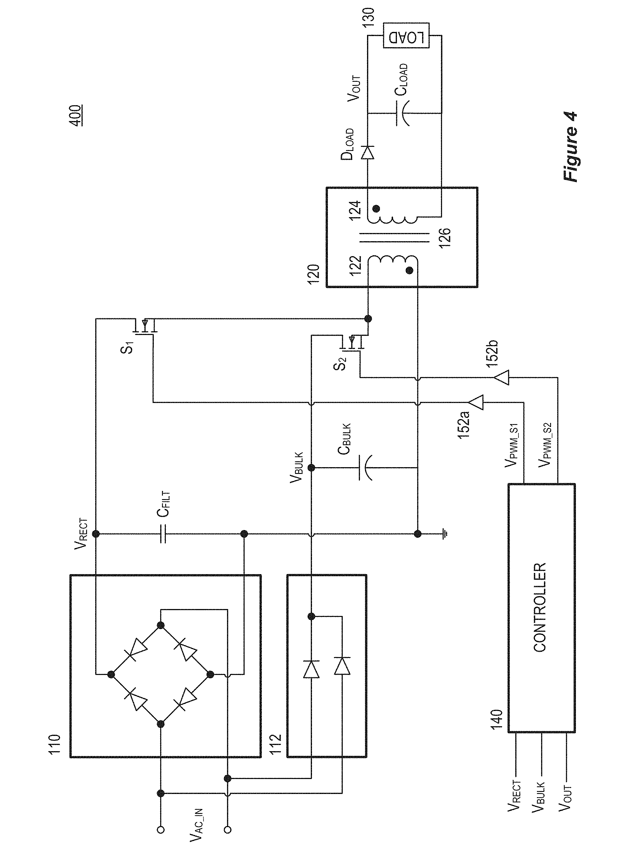
[0052] FIG. 4 illustrates a power converter 400 that is similar to that of FIG. 1. Only those aspects and components that differ from FIG. 1 will be described below. The primary difference for the power converter 400 is that the diode D.sub.1 illustrated in FIG. 1 is replaced with a second rectifier 112, which includes two diodes. This configuration offers the advantage that one diode drop is eliminated, thereby improving efficiency. A disadvantage of the power converter 400 is that it requires an additional diode relative to the power converter 100 of FIG. 1.
[0053] Another difference is that a filter capacitor C.sub.FILT is coupled across the rectified voltage node V.sub.RECT and ground. The filter capacitor C.sub.FILT is used to filter high-frequency noise from the first rectified voltage node V.sub.RECT. Note that the filter capacitor C.sub.FILT serves an entirely different purpose than the bulk capacitor C.sub.BULK, which stores substantial amounts of energy, and that the capacitance of the capacitor C.sub.FILT is significantly smaller than that of the bulk capacitor C.sub.BULK, e.g., by several orders of magnitude. Whereas the bulk capacitor C.sub.BULK, stores energy from an AC source with a fairly low frequency, e.g., 50 Hz or 60 Hz, the filter capacitor C.sub.FILT removes unwanted noise caused by the fast switching, which is typically 100 KHz or higher, of the power switches S.sub.1, S.sub.2. The filter capacitor C.sub.FILT typically has a capacitance of 100 nF or less, and is not a significant portion of the power converter size. A similar filter capacitor may be desired in the other power converter circuits described herein.
Power Converter with Switching on Ground Side of Transformer
[0054] FIG. 5 illustrates a power converter 500 that differs from that of FIG. 1 primarily in that power is switched on the ground side of the transformer 120, and the power selection is made between two voltage nodes on the negative side of the primary-side winding 122. The first power switch S.sub.1 couples power to the primary-side winding 122 from the first rectified voltage node V.sub.RECT by switching the connection to a ground node V.sub.RECT.sub._.sub.SS that is coupled to the negative side of the rectifier 110. A bulk capacitor C.sub.BULK is connected between the first rectified voltage node V.sub.RECT and a diode D.sub.1 at a voltage node V.sub.BULK.sub._.sub.SS, with the diode D.sub.1 further being connected to the ground node V.sub.RECT.sub._.sub.SS. The second power switch S.sub.2 couples power to the primary-side winding 122 from the first rectified voltage node V.sub.RECT by switching the connection to the second ground node V.sub.BULK.sub._.sub.SS, which is tied to the bulk capacitor C.sub.BULK. Such a configuration has the advantage that the switch drivers 552a, 552b are ground-referenced and may be driven by a low-voltage control signal. However, this configuration has the disadvantage that the "dotted" terminal of the primary-side winding 122 is floating when the power switches S.sub.1, S.sub.2 are open, meaning that the transformer 120 will be more susceptible to noise, i.e., the output from the secondary winding 124 may be noisier than a configuration in which the primary-side winding 122 is always grounded. Power Converter Using Bi-Directional Switch to Limit Voltage at Bulk Capacitor
[0055] FIG. 6 illustrates a power converter 600 in which the diode D.sub.1 of FIG. 1 has been replaced with a current-blocking device S.sub.BLK. Whereas the diode D.sub.1 is only capable of blocking current flow in one direction, the current-blocking device S.sub.BLK is preferably able to block current flow in either direction through it. The current-blocking device S.sub.BLK may be a bi-directional switch as may be constructed, e.g., using two back-to-back MOSFETs or similar. A configuration using such a bi-directional switch provides several potential advantages as compared to the power converters 100, 400 of FIGS. 1 and 4 which uses diodes, which are passive uni-directional current-blocking devices.
[0056] Bi-directional switches, such as the current-blocking device S.sub.BLK, may replace the diodes within the second rectification circuit 112 of FIG. 4, the diode D.sub.1 in FIG. 5, or similar diodes in other power converter topologies that use the techniques herein. Unlike a diode, use of the bi-directional switch S.sub.BLK requires a control signal V.sub.CTRLS.sub.BLK that determines when the switch S.sub.BLK should conduct. In order to mimic the diode D.sub.1, the controller 640 generates the control signal V.sub.CTRL.sub._.sub.SBLK such that the bi-directional switch S.sub.BLK conducts only when the first rectified voltage V.sub.RECT is greater than the second rectified voltage V.sub.BULK. The control signal V.sub.CTRL.sub._.sub.SBLK generated by the controller 640 is provided to a control terminal, e.g. a gate or gates, of the bi-directional switch S.sub.BLK via the driver 152c. Many of the advantages provided by the bi-directional switch S.sub.BLK rely upon control techniques that are more complex than merely mimicking diode operation, and are described further below.
[0057] The switch S.sub.BLK, whether it is bi-directional or not, typically has lower conduction losses than a diode, leading to improved efficiency of the power converter 600 as compared to the power converters using a diode in this capacity. The switch S.sub.BLK may be pulsed as the rectified voltage V.sub.RECT rises, so as to limit inrush current at least as provided via the second switch S.sub.2. Yet another advantage is that a bi-directional switch S.sub.BLK may limit the maximum voltage seen by the bulk capacitor C.sub.BULK and the second switch S.sub.2. By appropriately limiting this maximum voltage, the voltage rating of the bulk capacitor C.sub.BULK may be decreased, which typically leads to a desirable reduction in the size of the bulk capacitor C.sub.BULK.
[0058] Use of the bi-directional switch S.sub.BLK for reducing the maximum required voltage rating of the bulk capacitor C.sub.BULK is particularly advantageous for the previously-described universal power converters. Such power converters are typically required to handle peak line voltages of approximately 340V, so as to support the 240 V.sub.RMS mains AC voltage used in much of the world. When providing some margin for lightening surges or other anomalies, the bulk capacitor typically must be sized for approximately 400V. Because the capacitance of the bulk capacitor C.sub.BULK is typically determined from requirements for a lower-voltage mains voltage, e.g., the 125V peak voltage illustrated in FIGS. 3A and 3B, the high voltage levels provided by a 240 V.sub.RMS mains AC voltage are not really necessary for driving the transformer 120. The controller 640 may control the bi-directional switch S.sub.BLK so as to limit the maximum voltage provided to the bulk capacitor C.sub.BULK, while still meeting the power requirements of the power converter 600.
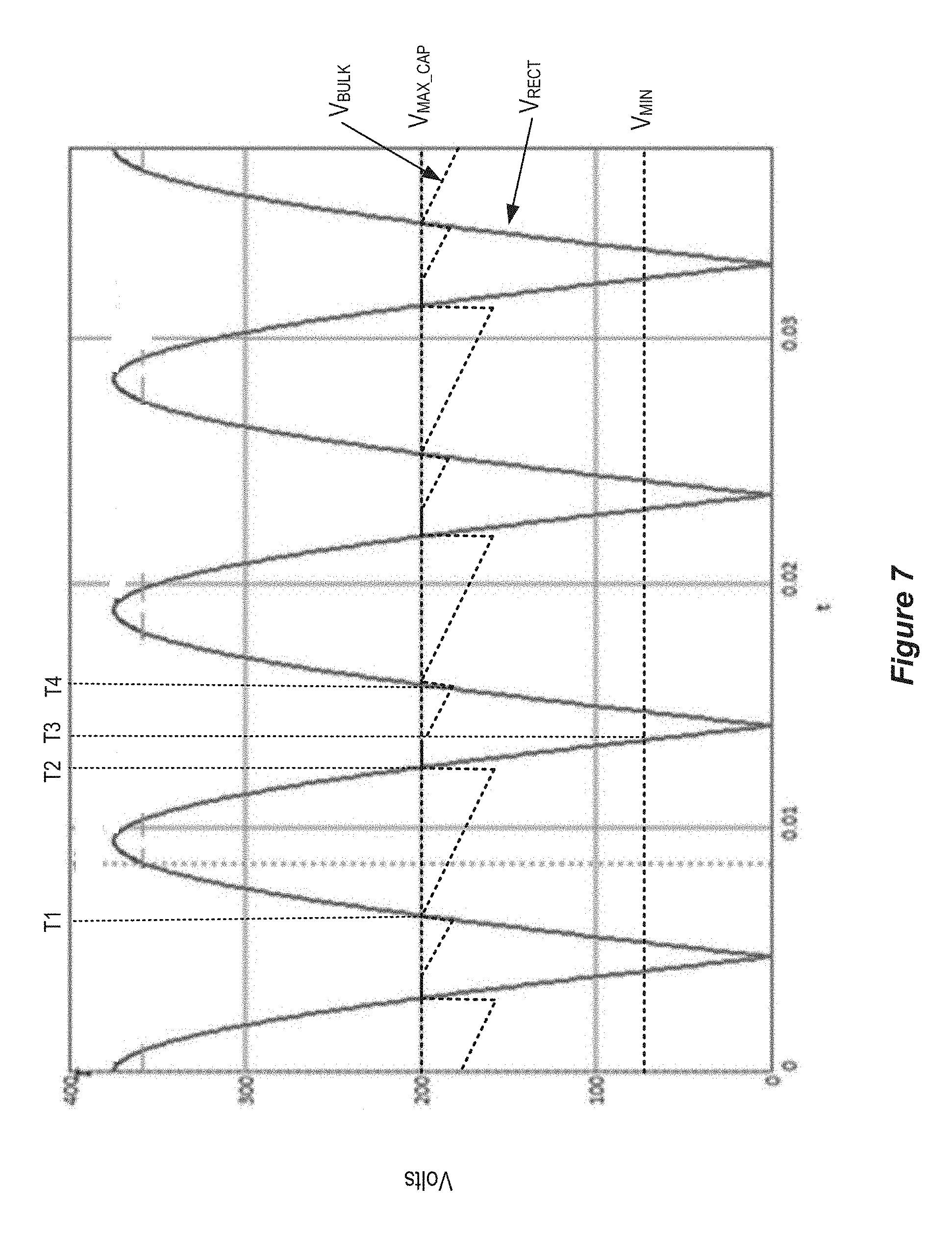
[0059] FIG. 7 illustrates waveforms corresponding to the first rectified voltage node V.sub.RECT and the second rectified voltage node V.sub.BULK within the power converter 600 of FIG. 6. For the illustrated scenario, the power converter is supplied by a high-voltage AC mains supply, wherein the rectifier 110 provides a peak voltage of approximately 375V. The transformer 120 requires a minimum voltage input V.sub.MIN of 86V, as in the scenarios illustrated in FIGS. 3A and 3B. The bulk capacitor C.sub.BULK has a maximum voltage rating V.sub.MAX.sub._.sub.CAP of 200V. As explained below, the controller 640 must control the bi-directional switch S.sub.BLK so as to ensure this maximum voltage rating is not violated.
[0060] At time t=T1, the bulk capacitor C.sub.BULK has been charged to a level of V.sub.BULK=200V. Responsive to detecting that the storage voltage V.sub.BULK (or, similarly, the first rectified voltage V.sub.RECT) has reached a maximum voltage threshold V.sub.MAX.sub._.sub.CAP, i.e., 200V for this example, the controller 640 disables the bi-directional switch S.sub.BUC at time t=T1, thereby preventing the storage voltage V.sub.BULK from rising above the maximum voltage threshold V.sub.MAX.sub._.sub.CAP. Between times t=T1 and T2, the controller 640 switches the second switch S.sub.2 so as to supply power to the transformer 120 from the bulk capacitor C.sub.BULK. At time t=T2, the controller 640 detects that the first rectified voltage V.sub.RECT has fallen below the maximum voltage threshold V.sub.MAX.sub._.sub.CAP (e.g., 200V). Responsive to this detection, the controller 640 enables the bi-directional switch S.sub.BLK at time t=T2 such that the switch S.sub.BUC begins conducting again and the bulk capacitor C.sub.BULK is charged. Shortly after time t=T2, e.g., when it is detected that the sensed storage voltage V.sub.BULK has risen to, or nearly to, the level of the sensed first rectified voltage V.sub.RECT, the controller 640 disables the bi-directional switch S.sub.BLK so as to maintain the charged voltage (e.g., slightly under 200V) on the bulk capacitor C.sub.BULK. Between this point in time and time t=T3, the first rectified voltage V.sub.RECT is used to power the transformer 120 by switching the first switch S.sub.1. In an alternative embodiment, the controller may alternate use of the first and second switches S.sub.1, S.sub.2, so as to maintain a smoother average voltage input to the transformer 120.
[0061] At time t=T3, the controller 640 detects that the first rectified voltage V.sub.RECT has fallen to the minimum voltage threshold V.sub.MIN. As similarly described regarding FIG. 3A, the controller 640 then disables the first switch S.sub.1, and begins switching the second switch S2 to supply power to the transformer 120 from the bulk capacitor C.sub.BULK. Between times t=T3 and t=T4, the storage voltage V.sub.BULK drops as energy from the bulk capacitor C.sub.BULK is depleted. At time t=T4, the controller 640 detects that the first rectified voltage V.sub.RECT has risen above the storage voltage V.sub.BULK. Responsive to this detection, the controller 640 enables the bi-directional switch S.sub.BLK such that it conducts and the bulk capacitor C.sub.BULK is charged. This state is maintained until the sensed storage voltage V.sub.BULK rises to the maximum voltage threshold V.sub.MAX.sub._.sub.CAP, at which point the bi-directional switch S.sub.BLK is disabled such that it does not conduct. During this interval just after time t=T4, the first switch S, may be switched or both switches S.sub.1, S.sub.2 may be switched, as described above in the "Alternative Switch Selection Techniques" section, to provide power to the primary-side winding 120. The above-described sequence of events starting at time t=T1 then repeats for each half-sinusoid of the rectified voltage V.sub.RECT.
[0062] For a scenario in which the peak value of the first rectified voltage V.sub.RECT remains below the maximum voltage threshold V.sub.MAX.sub._.sub.CAP, the bi-directional switch S.sub.BLK may operate to merely mimic a diode. The resultant voltage waveforms would be very similar to the waveforms illustrated in FIG. 3A.
Power Converter Operation During Low-Power Modes
[0063] Use of the bi-directional switch S.sub.BLK provides additional advantages for a power converter operating in a low-power (e.g., burst) mode of operation. The controller 640 may detect, e.g., from the load voltage V.sub.OUT or from sensing a current provided to the load 130, that the load 130 is operating in a state in which a very low level of power is needed. For example, the load 130 may be in a standby operational mode. During low-power operation of the power converter 600, it may be possible to provide energy packets to the transformer 120, e.g., by providing a pulse to the first switch S.sub.1 or the second switch S2, at a rate that is lower than the frequency of the input power source (e.g., 50 Hz, 60 Hz). Preferably, during such light-load conditions, the power converter 600 may leave S.sub.1 disabled and only use the second switch S2, and the energy stored on the bulk capacitor C.sub.BULK, for several cycles of the input source voltage.
[0064] Under light-load conditions and using the techniques described above, the controller 640 (e.g., particularly a PID controller therein) may generate very short pulses to control the second switch S.sub.2 using the control signal V.sub.PWM.sub._.sub.S2. The pulses may be so short as to violate minimum on-times for the second switch S.sub.2. (For example, MOSFETs often have a minimum on-time duration.) Furthermore, the short switch pulses and resultant switching frequency may generate undesirable audible noise. These problems may be addressed by supplying a lower voltage level to the primary winding 120 during low-power mode as compared to a normal operational mode of the power converter 600. By providing energy pulses having a lower voltage, the time interval of the required pulses will be longer, thereby meeting any minimum on-time for the second power switch S2 and leading to a switching frequency that is outside the audible range (e.g., outside approximately 20 Hz to 20 kHz).
[0065] As explained in FIG. 7 and its description, the bi-directional switch S.sub.BLK is used to limit the voltage provided to the second rectified voltage node V.sub.BULK to a range between V.sub.MIN (e.g., 86V) and the maximum voltage threshold V.sub.MAX.sub._.sub.CAP (e.g., 200V). The minimum voltage V.sub.MIN described previously represents a minimum voltage required by the DC/DC power converter during normal operational mode in order to meet the power requirements of the load 130. During the low-power mode of operation, this minimum voltage does not apply.
[0066] During low-power operation, the controller 640 may control the bi-directional switch S.sub.BLK in much the same manner as described in conjunction with FIG. 7, except that different minimum and maximum voltage thresholds are defined for low-power operation. FIG. 7 shows that the voltage provided to the primary winding 122 is within the range of V.sub.MIN=86V to the maximum voltage threshold V.sub.MAX.sub._.sub.CAP=200V. In a preferred sub-embodiment, the controller 640, during low-power operation, controls the bi-directional switch S.sub.BULK so as to maintain a voltage at the second rectified voltage node V.sub.BULK that is within a range that is lower in magnitude than the normal operational mode, e.g., this voltage may be kept within a range of 20V to 25V rather than 86V to 200V. This is accomplished by only enabling the bi-directional switch S.sub.BLK when the controller 640 detects that the voltage at the first rectified voltage node V.sub.RECT is within the range 20 to 25V. With the storage voltage V.sub.BULK within this range, the controller 640 may use the second switch S.sub.2 to provide power to the primary-side winding 122 from the bulk capacitor C.sub.BULK during low-power operational mode.
Power Converters with Multiple Sets of Bulk Capacitors and Switches
[0067] FIG. 8 illustrates a power converter 800 that is a variation of the power converter 100 of FIG. 1. For ease of illustration, only the primary-side winding 122 of the transformer is shown, with the understanding that the rest of the transformer and the components on the secondary side of the transformer would be similar to the circuits described previously. Rather than having one circuit block comprising a diode D.sub.1, a bulk capacitor C.sub.BULK, and a power switch S.sub.2, the illustrated power converter 800 includes multiple such circuit blocks. More particularly, a second circuit block comprising a second diode D.sub.2, a second bulk capacitor C.sub.BULK2, and a third power switch S.sub.3 are shown. Such circuit blocks may be repeated up to an n.sup.th circuit block comprising a diode D.sub.n, a bulk capacitor C.sub.BULKn, and a power switch S.sub.n+1. Each power switch S.sub.2, S.sub.3, . . . S.sub.n+1 has an associated driver 152b, 152c . . . 152n that is driven by a control signal V.sub.PWM.sub._.sub.S2, V.sub.PWM.sub._.sub.S3, . . . V.sub.PWM.sub._.sub.Sn+1.
[0068] The controller 840 inputs voltages corresponding to multiple second rectified voltage nodes V.sub.BULK1, V.sub.BULK2, . . . V.sub.BULKn. The controller 840 operates in a similar manner as described in conjunction with FIG. 3A, except that the selection of a switch and bulk capacitor sequences through each of the circuit blocks during the interval when the first rectified voltage node V.sub.RECT is below the minimum voltage threshold V.sub.MIN. This will be explained with reference to FIG. 3A, though not all of the described waveforms are illustrated in this figure. For operation that is not explicitly described, the operation described in conjunction with FIG. 3A may be presumed.
[0069] From time t=0 to t=T1, the controller 840 switches the first switch S.sub.1 so as to provide power to the primary-side winding 122 from the first rectified voltage node V.sub.RECT. At time t=T1, the controller 840 detects that the voltage of the first rectified voltage node V.sub.RECT has dropped below the minimum allowed voltage V.sub.MIN. In response to this detection, the controller 840 selects the second switch S.sub.2 for switching, such that power is provided from the first bulk capacitor C.sub.BULK1. (The first switch S.sub.1 is turned off so that it does not conduct.) Subsequent to this, the voltage V.sub.BULK1 of the first bulk capacitor C.sub.BULK is depleted to the minimum allowed voltage V.sub.MIN. Upon detecting this, the controller 840 turns off the second switch S.sub.2 and begins switching the third switch S.sub.3, such that power is provided from the second bulk capacitor C.sub.BULK2 rather than the first rectified voltage node V.sub.RECT or the first bulk capacitor C.sub.BULK1. Such operation is repeated until the (n+1).sup.st power switch S.sub.n+1 is used to supply power from the n.sup.th bulk capacitor C.sub.BULKn. Under less than full-load conditions, some of the bulk capacitors may go unused during an input switch cycle.
[0070] The use of the bulk capacitors capacitor C.sub.BULK1 . . . C.sub.BULKn ceases at time t=T2, when the controller 840 detects that the first rectified voltage V.sub.RECT has risen above the minimum allowed voltage V.sub.MIN. As in the operation described in conjunction with FIG. 3A, between times t=T2 and t=T4 the controller 840 switches the first switch S.sub.1 so as to provide power to the primary-side winding 122 from the rectified voltage node V.sub.RECT. From time t=T2 to t=T3, the first through n.sup.th diodes D.sub.1, D.sub.2, . . . D.sub.n charge each of the bulk capacitors C.sub.BULK1, C.sub.BULK2, . . . C.sub.BULKn.
Method for Controlling Power Converter with Separate Rectified Voltage Nodes
[0071] FIG. 9 illustrates a method 900 for supplying power to a primary-side winding of a power converter, such as the power converter 100 of FIG. 1. This method may be implemented, e.g., within a controller of the power converter, such as the controller 140 of FIG. 1. The techniques of this method 900 are similar to the techniques described above for the power converter 100 of FIG. 1, and may be implemented within such a power converter. While not described below, it should be recognized that the method 900 may be readily modified to implement the techniques described in conjunction with FIGS. 4-6 and 8.
[0072] In a first step 910, a voltage V.sub.RECT at a first rectified voltage node is sensed (measured). This may be done using an analog-to-digital converter (ADC) within a controller, as is known in the art. The sensed voltage V.sub.RECT is compared 920 with a minimum voltage V.sub.MIN that is allowed to be input to a transformer of the power converter. As long as the sensed voltage V.sub.RECT is greater than the voltage threshold V.sub.MIN allowed, power is supplied 930 to the transformer from the rectified voltage node by switching a first switch that couples power from the first rectified voltage node to the transformer.
[0073] Once the sensed voltage V.sub.RECT falls below the voltage threshold V.sub.MIN, operation of the power converter is changed to supply 940 power to the transformer from a bulk capacitor, such as the capacitor C.sub.BULK of FIG. 1, by switching a second switch. The voltage V.sub.RECT at the first rectified voltage node is measured 950 again and compared 960 against a second threshold voltage (V.sub.MIN+V.sub.HYST). The hysteresis value V.sub.HYST is optional, i.e., may be zero. When included, the hysteresis value V.sub.HYST prevents undesirable vacillations between operation using the first rectified voltage node and the bulk capacitor, wherein those vacillations are caused by noise on the measured voltage V.sub.RECT. As long as the measured voltage V.sub.RECT remains below this second threshold voltage (V.sub.MIN+V.sub.HYST), power continues to be supplied 940 from the bulk capacitor C.sub.BULK.
[0074] Once the sensed voltage V.sub.RECT rises above the second threshold voltage (V.sub.IN+V.sub.HYST), operation of the power converter is changed to supply 930 power from the first rectified voltage node using the first switch, as described previously.
[0075] Such operation continues as long as the power converter is in use. Applying the method 900 of FIG. 9 to a power converter having a rectified voltage as illustrated in FIG. 3A, the transition to use the bulk capacitor and the second switch would occur at time t=T1, when it is detected that the sensed voltage V.sub.RECT has fallen to the minimum voltage V.sub.MIN. The transition back to using the first rectified voltage node and the first switch would occur at time t=T2, when the sensed voltage V.sub.RECT has risen to the minimum voltage V.sub.MIN plus, optionally, a hysteresis voltage V.sub.HYST. Such transitions should occur twice per each half-sinusoidally shaped interval of the sensed voltage V.sub.RECT at the rectified voltage node.
[0076] As used herein, the terms "having," "containing," "including," "comprising," and the like are open-ended terms that indicate the presence of stated elements or features, but do not preclude additional elements or features. The articles "a," "an" and "the" are intended to include the plural as well as the singular, unless the context clearly indicates otherwise.
[0077] It is to be understood that the features of the various embodiments described herein may be combined with each other, unless specifically noted otherwise.
[0078] Although specific embodiments have been illustrated and described herein, it will be appreciated by those of ordinary skill in the art that a variety of alternate and/or equivalent implementations may be substituted for the specific embodiments shown and described without departing from the scope of the present invention. This application is intended to cover any adaptations or variations of the specific embodiments discussed herein. Therefore, it is intended that this invention be limited only by the claims and the equivalents thereof.
* * * * *
D00000
D00001
D00002
D00003
D00004
D00005
D00006
D00007
D00008
D00009
XML
uspto.report is an independent third-party trademark research tool that is not affiliated, endorsed, or sponsored by the United States Patent and Trademark Office (USPTO) or any other governmental organization. The information provided by uspto.report is based on publicly available data at the time of writing and is intended for informational purposes only.
While we strive to provide accurate and up-to-date information, we do not guarantee the accuracy, completeness, reliability, or suitability of the information displayed on this site. The use of this site is at your own risk. Any reliance you place on such information is therefore strictly at your own risk.
All official trademark data, including owner information, should be verified by visiting the official USPTO website at www.uspto.gov. This site is not intended to replace professional legal advice and should not be used as a substitute for consulting with a legal professional who is knowledgeable about trademark law.