Electrostatic Discharge Protection Circuit With A High Turn-on Speed
Lai; Chih-Wei ; et al.
U.S. patent application number 16/033235 was filed with the patent office on 2019-05-30 for electrostatic discharge protection circuit with a high turn-on speed. The applicant listed for this patent is eMemory Technology Inc.. Invention is credited to Hsin-Kun Hsu, Chih-Wei Lai, Yun-Jen Ting, Yi-Han Wu.
| Application Number | 20190165572 16/033235 |
| Document ID | / |
| Family ID | 63857699 |
| Filed Date | 2019-05-30 |


| United States Patent Application | 20190165572 |
| Kind Code | A1 |
| Lai; Chih-Wei ; et al. | May 30, 2019 |
ELECTROSTATIC DISCHARGE PROTECTION CIRCUIT WITH A HIGH TURN-ON SPEED
Abstract
An electrostatic discharge (ESD) protection circuit includes an ESD release transistor, at least one stress release transistor, a control circuit, and a voltage division circuit. The ESD release transistor is coupled to a reference voltage terminal of a circuit to be protected. The at least one stress release transistor is coupled between a voltage input terminal of the circuit to be protected and the ESD release transistor. The control circuit turns off the ESD release transistor during a normal operation, and turns on the ESD release transistor during a positive ESD zapping. The voltage division circuit provides at least one divisional voltage for turning on the at least one stress release transistor during the normal operation and the positive ESD zapping.
| Inventors: | Lai; Chih-Wei; (Taipei City, TW) ; Ting; Yun-Jen; (Hsinchu County, TW) ; Wu; Yi-Han; (Taichung City, TW) ; Hsu; Hsin-Kun; (Hsinchu County, TW) | ||||||||||
| Applicant: |
|
||||||||||
|---|---|---|---|---|---|---|---|---|---|---|---|
| Family ID: | 63857699 | ||||||||||
| Appl. No.: | 16/033235 | ||||||||||
| Filed: | July 12, 2018 |
Related U.S. Patent Documents
| Application Number | Filing Date | Patent Number | ||
|---|---|---|---|---|
| 62590402 | Nov 24, 2017 | |||
| Current U.S. Class: | 1/1 |
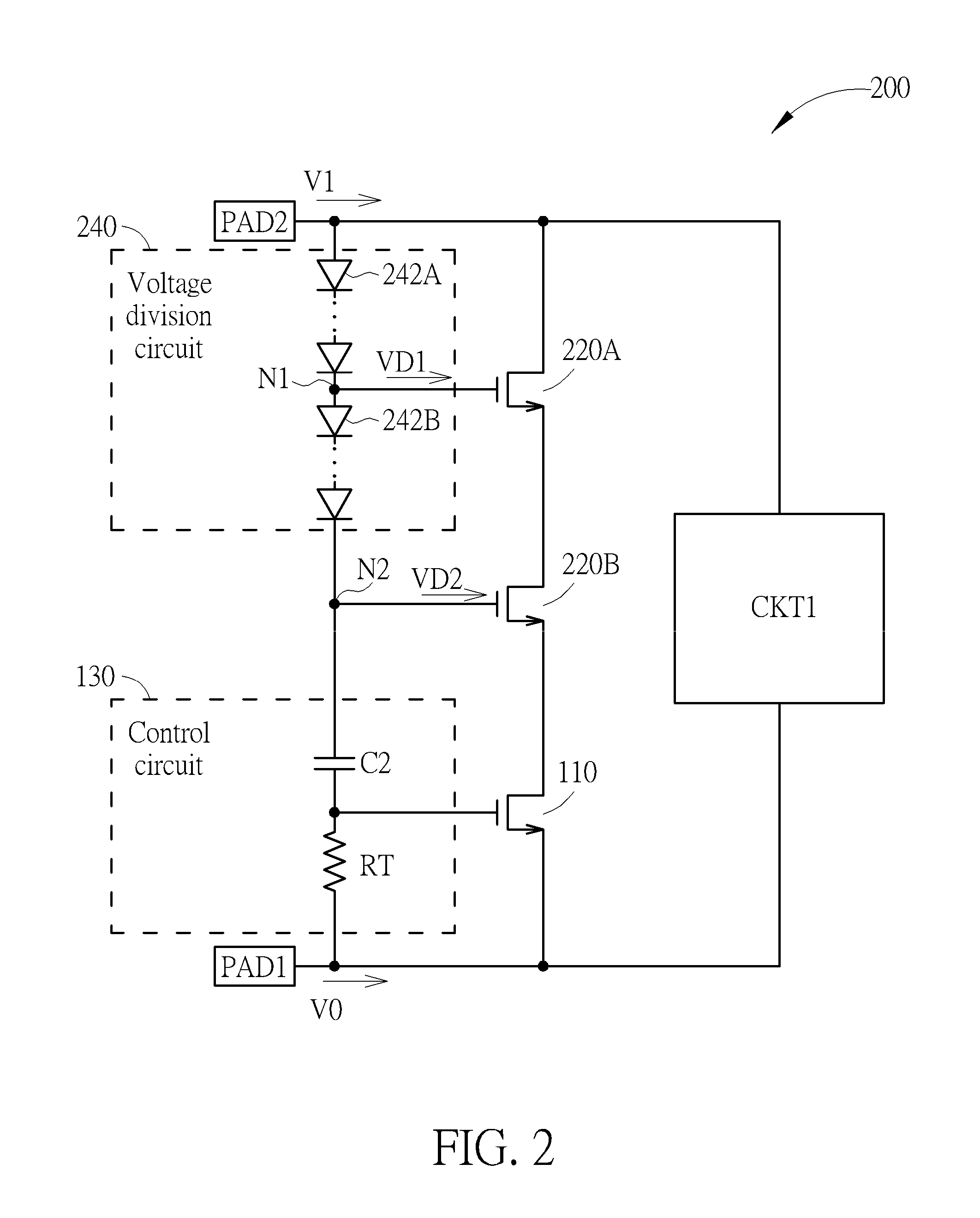
| Current CPC Class: | G11C 11/5621 20130101; H01L 29/0649 20130101; H01L 29/42328 20130101; H04L 9/0877 20130101; H04L 9/0866 20130101; H04L 9/3278 20130101; G11C 16/0483 20130101; H01L 27/11524 20130101; H02H 9/046 20130101; H04L 9/3073 20130101; H01L 29/4916 20130101; H04L 63/062 20130101 |
| International Class: | H02H 9/04 20060101 H02H009/04 |
Claims
1. An electrostatic discharge (ESD) protection circuit comprising: an ESD release transistor coupled to a reference voltage terminal configured to provide a reference voltage for a circuit to be protected; at least one stress release transistor coupled between a voltage input terminal configured to provide an input voltage for the circuit to be protected and the ESD release transistor; a control circuit configured to turn off the ESD release transistor during a normal operation, and turn on the ESD release transistor during a positive ESD zapping; and a voltage division circuit configured to provide at least one divisional voltage according to the input voltage provided from the voltage input terminal for turning on the at least one stress release transistor during the normal operation and the positive ESD zapping.
2. The electrostatic discharge protection circuit of claim 1, wherein the voltage division circuit comprises: a first reference voltage node coupled to a control terminal of a first stress release transistor of the at least one stress release transistor, and configured to provide a first divisional voltage; and a first set of diodes coupled in series between the voltage input terminal and the first reference voltage node.
3. The electrostatic discharge protection circuit of claim 2, wherein the voltage division circuit further comprises: a first capacitor coupled in parallel with the first set of diodes.
4. The electrostatic discharge protection circuit of claim 2, wherein the control circuit comprises: a second capacitor having a first terminal coupled to the first reference voltage node, and a second terminal coupled to a control terminal of the ESD release transistor.
5. The electrostatic discharge protection circuit of claim 4, wherein the second capacitor is implemented by a metal-oxide-semiconductor transistor.
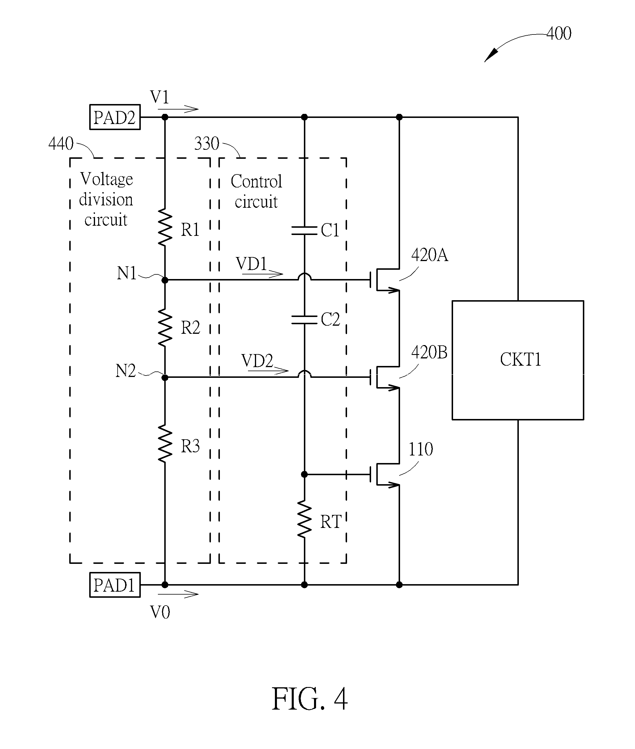
6. The electrostatic discharge protection circuit of claim 4, wherein the control circuit further comprises: a transient resistor coupled between the second terminal of the second capacitor and the reference voltage terminal.
7. The electrostatic discharge protection circuit of claim 2, wherein the voltage division circuit further comprises: a second reference voltage node coupled to a control terminal of a second stress release transistor of the at least one stress release transistor, and configured to provide a second divisional voltage; and a second set of diodes coupled in series between the first reference voltage node and the second reference voltage node.
8. The electrostatic discharge protection circuit of claim 1, wherein the voltage division circuit comprises: a first reference voltage node coupled to a control terminal of a first stress release transistor of the at least one stress release transistor, and configured to provide a first divisional voltage; a first resistor coupled between the voltage input terminal and the first reference voltage node; and a second resistor coupled between the first reference voltage node and the reference voltage terminal.
9. The electrostatic discharge protection circuit of claim 8, wherein the control circuit comprises: a first capacitor having a first terminal coupled to the voltage input terminal, and a second terminal; and a second capacitor having a first terminal coupled to the second terminal of the first capacitor, and a second terminal coupled to a control terminal of the ESD release transistor.
10. The electrostatic discharge protection circuit of claim 9, wherein the control circuit further comprises: a transient resistor coupled between the second terminal of the second capacitor and the reference voltage terminal.
11. The electrostatic discharge protection circuit of claim 8, wherein the voltage division circuit further comprises: a second reference voltage node coupled to the second resistor and a control terminal of a second stress release transistor of the at least one stress release transistor, and configured to provide a second divisional voltage; and a third resistor coupled between the second reference voltage node and the reference voltage terminal.
12. The electrostatic discharge protection circuit of claim 1, wherein the at least one stress release transistor and the ESD release transistor are N-type transistors; a body terminal of the at least one stress release transistor and a body terminal of the ESD release transistor are coupled to the reference voltage terminal; and during a negative ESD zapping, an ESD release current flows from the reference voltage terminal to the voltage input terminal through the body terminal of the at least one stress release transistor and the body terminal of the ESD release transistor.
Description
CROSS REFERENCE TO RELATED APPLICATIONS
[0001] This non-provisional application claims priority of US provisional application No. 62/590,402, filed on Nov. 24, 2017, included herein by reference in its entirety.
BACKGROUND OF THE INVENTION
1. Field of the Invention
[0002] This invention is related to an electrostatic discharge protection circuit, and more particularly, an electrostatic discharge protection circuit with a high turn-on speed.
2. Description of the Prior Art
[0003] When two electrically charged objects are in contact or are shorted to each other, the electrical charges in one object will flow to another object through a discharging path, causing electrostatic discharge. The electrostatic discharge can generate huge currents in a very short time and can damage integrated circuits. Since the human body, machines used to package integrated circuits, and instruments for testing integrated circuits are all common charged bodies, irreversible harm can be caused to the circuit once the charged body contacts with the circuit and discharges to the circuit. Therefore, electrostatic discharge protection circuits are usually adopted to provide low resistance discharge paths for the huge ESD currents to pass by and to protect the integrated circuits from being blown out.
[0004] Also, in some cases, the ESD protection devices may be manufactured by a low voltage process as the circuit to be protected. Therefore, to endure the high operational voltages required by the circuit to be protected during normal operations, the discharging path provided by the ESD protection circuit usually contains more than one transistor, preventing the transistors from breaking down. However, the non-uniform turn-on issue caused by cascode structure of the transistors will lower the ability of discharge and the efficiency of protection. Furthermore, since the discharging path is partly provided by the parasitic bipolar junction transistors in the cascode structure, the turn-on speed of the ESD circuit is rather slow. Also, if the transistors are not turned on soon enough, the discharging current will flow into the circuit to be protected before the transistors are turned on, causing damage to the circuit to be protected.
SUMMARY OF THE INVENTION
[0005] One embodiment of the present invention discloses an electrostatic discharge (ESD) protection circuit. The ESD protection circuit includes an ESD release transistor, at least one stress release transistor, a control circuit, and a voltage division circuit.
[0006] The ESD release transistor is coupled to a reference voltage terminal of a circuit to be protected. The at least one stress release transistor is coupled between a voltage input terminal of the circuit to be protected and the ESD release transistor. The control circuit turns off the ESD release transistor during a normal operation, and turns on the ESD release transistor during a positive ESD zapping. The voltage division circuit provides at least one divisional voltage according to an input voltage received from the voltage input terminal for turning on the at least one stress release transistor during the normal operation and the positive ESD zapping.
[0007] These and other objectives of the present invention will no doubt become obvious to those of ordinary skill in the art after reading the following detailed description of the preferred embodiment that is illustrated in the various figures and drawings.
BRIEF DESCRIPTION OF THE DRAWINGS
[0008] FIG. 1 shows an electrostatic discharge (ESD) protection circuit according to one embodiment of the present invention.
[0009] FIG. 2 shows an ESD protection circuit according to another embodiment of the present invention.
[0010] FIG. 3 shows an ESD protection circuit according to another embodiment of the present invention.
[0011] FIG. 4 shows an ESD protection circuit according to another embodiment of the present invention.
DETAILED DESCRIPTION
[0012] FIG. 1 shows an electrostatic discharge (ESD) protection circuit 100 according to one embodiment of the present invention. The ESD protection circuit 100 includes an ESD release transistor 110, a stress release transistor 120, a control circuit 130, and a voltage division circuit 140.
[0013] The ESD release transistor 110 is coupled to a reference voltage terminal PAD1 for providing a reference voltage V0 to the circuit CKT1 to be protected. The stress release transistor 120 is coupled between a voltage input terminal PAD2 for providing an input voltage V1 for the circuit CKT1 and the ESD release transistor 110. In some embodiments, the input voltage V1 provided by the voltage input terminal PAD2 can be the high operation voltage required by the circuit CKT1, and the reference voltage V0 provided by the reference voltage terminal PAD1 can be the ground voltage of the circuit CKT1.
[0014] In some embodiments, due to the requirement for low power consumption and low cost, the circuit CKT1 may be manufactured by a low voltage process, for example, the components of the circuit CKT1 are normally operated under 1.8V. In this case, to simplify the manufacturing process, the ESD protection circuit 100 may also be manufactured by the same low voltage process. However, in some applications, the circuit CKT1 may still require high operation voltages, such as over 6V, for some specific operations, such as programming a non-volatile memory cell, and the input voltage V1 may be higher than the breakdown voltage of the ESD release transistor 110.
[0015] To prevent the ESD release transistor 110 from breaking down, the voltage division circuit 140 can provide a first divisional voltage VD1 according to the input voltage V1 for controlling the stress release transistor 120. The first divisional voltage VD1 is an intermediate voltage lower than the input voltage V1 and higher than the reference voltage V0, and can keep the stress release transistor 120 turned on during a normal operation. Therefore, the cross voltages of the stress release transistor 120 and the ESD release transistor 110 can be controlled within safe regions.
[0016] Also, to prevent the ESD protection circuit 100 from generating leakage current during the normal operation, the control circuit 130 can turn off the ESD release transistor 110 during the normal operation. However, during a positive ESD zapping, that is, when the input voltage V1 is raised drastically due to ESD, the control circuit 130 would turn on the ESD release transistor 110. Since the stress release transistor 120 is always turned on, the ESD protection circuit 100 can provide the discharge path immediately by turning on the ESD release transistor 110 during the positive ESD zapping.
[0017] In FIG. 1, the voltage division circuit 140 includes a first reference voltage node N1 and a set of diodes 142. The first reference voltage node N1 is coupled to a control terminal of the stress release transistor 120, and can provide the first divisional voltage VD1. The set of diodes 142 are coupled in series between the voltage input terminal PAD2 and the first reference voltage node N1. That is, the voltage division circuit 140 can provide the first divisional voltage VD1 through the first reference voltage node N1. For example, in FIG. 1, the set of diodes 142 can be forward biased so each of the diodes 142 would contribute a voltage gap about 0.7V, that is, the forward biased voltage of a diode. Therefore, by adjusting the number of diodes in the set of diodes 142, the first divisional voltage VD1 can also be adjusted accordingly. For example, the input voltage V1 can be 6V, and the voltage division circuit 140 can include four diodes to create a voltage gap of 2.8V between the input voltage V1 and the first divisional voltage VD1. Therefore, the first divisional voltage VD1 would be 3.2V, and the stress release transistor 120 can be turned on during the normal operation.
[0018] In addition, in FIG. 1, the voltage division circuit 140 further includes a first capacitor C1 coupled in parallel with the set of diodes 142. In this case, when the input voltage V1 is raised drastically during the positive ESD zapping, the first capacitor C1 can help to raise the level of the first divisional voltage VD1 quickly. However, in some embodiments, if the parasitic capacitors of the set of diodes 142 are quite small and the first divisional voltage VD1 can be changed with the input voltage V1 soon enough, then the first capacitor C1 may not be required. In this case, the first capacitor C1 may be omitted according to the system requirement.
[0019] The control circuit 130 includes a second capacitor C2 and a transient resistor RT. The second capacitor C2 has a first terminal coupled to the first reference voltage node N1, and a second terminal coupled to a control terminal of the ESD release transistor 110. In FIG. 1, the second capacitor C2 can be implemented by a metal-oxide-semiconductor transistor. In this case, the first terminal of the second capacitor C2 may be the source and drain of the transistor, and the second terminal of the second capacitor C2 may be the gate of the transistor. The transient resistor RT is coupled between the second terminal of the second capacitor C2 and the reference voltage terminal PAD1.
[0020] During the normal operation, the second capacitor C2 can be seemed as an open circuit. Therefore, the voltage at the second terminal of the second capacitor C2 would be pulled down by the transient resistor RT to the reference voltage V0, turning off the ESD release transistor 110.
[0021] However, during the positive ESD zapping, the input voltage V1 is raised to a high voltage drastically in a short period of time. In this case, the second capacitor C2 can be seemed as a short circuit. Therefore, the voltage at the second terminal of the second capacitor C2 is also raised, turning on the ESD release transistor 110. Since the stress release transistor 120 and the ESD release transistor 110 are both turned on during the positive ESD zapping, the ESD protection circuit 100 is able to provide a discharging path accordingly. Also, by properly selecting the transient resistor RT and the second capacitor C2, the turn-on duration and turn-on speed of the ESD release transistor 110 can be adjusted to desired values.
[0022] Furthermore, in some embodiments, the holding voltage of the ESD protection circuit 100 can be adjusted by selecting the width of the stress release transistor 120 and the ESD release transistor 110. For example, the width of the stress release transistor 120 and the ESD release transistor 110 may be increased to lower the holding voltage according to the system requirement.
[0023] In addition to providing the discharging path by turning on the stress release transistor 120 and the ESD release transistor 110, the ESD protection circuit 100 may also provide a discharging path with the parasitic bipolar junction transistors residing in the stress release transistor 120 and the ESD release transistor 110 during the positive ESD zapping. Therefore, the discharging capability of the ESD protection circuit 100 can be further improved.
[0024] In FIG. 1, the stress release transistor 120 and the ESD release transistor 110 are N-type transistors, and the body terminal of the stress release transistor 120 and the body terminal of the ESD release transistor 110 are coupled to the reference voltage terminal PAD1. Therefore, during a negative ESD zapping, when the input voltage V1 is drastically pulled down to be much lower than the reference voltage V0, the ESD release current will flow from the reference voltage terminal PAD1 to the voltage input terminal PAD2 through the body terminal of the stress release transistor 120 and the body terminal of the ESD release transistor 110. Therefore, the ESD protection circuit 100 is also capable of relieving the negative ESD zapping.
[0025] In some embodiments, if the input voltage V1 is much higher than the breakdown voltages of the stress release transistor 120 and the ESD release transistor 110, then the ESD protection circuit 100 may require more stress release transistors to relieve the cross voltages on the transistors.
[0026] FIG. 2 shows an ESD protection circuit 200 according to another embodiment of the present invention. The ESD protection circuits 100 and 200 have similar structures and can be operated by similar principles. However, the ESD protection circuit 200 includes two stress release transistor 220A and 220B. Also, the voltage division circuit 240 includes two reference voltage nodes N1 and N2, and two sets of diodes 242A and 242B.
[0027] The first set of diodes 242A can provide the first divisional voltage VD1 through the first reference voltage node N1 to turn on the first stress release transistor 220A. The second reference voltage node N2 is coupled to a control terminal of the second stress release transistor 220B, and can provide a second divisional voltage VD2. The second set of diodes 242B are coupled in series between the first reference voltage node N1 and the second reference voltage node N2.
[0028] Since the ESD protection circuit 200 includes more stress release transistors than the ESD protection circuit 100, the ESD protection circuit 200 is able to endure higher input voltage. That is, the ESD protection circuit may include more than one stress release transistor according to the system requirement.
[0029] FIG. 3 shows an ESD protection circuit 300 according to another embodiment of the present invention. The ESD protection circuit 300 includes an ESD release transistor 110, a stress release transistor 120, a control circuit 330, and a voltage division circuit 340. The ESD protection circuits 100 and 300 can be operated with similar principles; however, the voltage division circuit 340 is implemented by resistors.
[0030] In FIG. 3, the voltage division circuit 340 includes a first reference voltage node N1, a first resistor R1 and a second resistor R2.
[0031] The first reference voltage node N1 is coupled to the control terminal of the stress release transistor 120, and can provide the first divisional voltage VD1. The first resistor R1 is coupled between the voltage input terminal PAD2 and the first reference voltage node N1. The second resistor R2 is coupled between the first reference voltage node N1 and the reference voltage terminal PAD1. That is, in ESD protection circuit 300, the voltage division circuit 340 can provide the first divisional voltage VD1 through the resistors R1 and R2. Therefore, by selecting the ratio of the resistors R1 and R2 properly, the desired divisional voltage VD1 can be generated. However, in some embodiments, the resistance of the resistors R1 and R2 should be rather high for reducing the leakage current.
[0032] Also, the control circuit 330 includes a first capacitor C1, a second capacitor C2, and a transient resistor RT. The first capacitor C1 has a first terminal coupled to the voltage input terminal PAD2, and a second terminal. The second capacitor C2 has a first terminal coupled to the second terminal of the first capacitor C1, and a second terminal coupled to a control terminal of the ESD release transistor 110. The transient resistor RT is coupled between the second terminal of the second capacitor C2 and the reference voltage terminal PAD1. In this case, the control circuit 330 can turn off the ESD release transistor 110 during the normal operation, and can turn on the ESD release transistor 110 during the positive ESD zapping when the input voltage V1 is raised drastically.
[0033] In FIG. 3, to simplify the manufacturing process, the first capacitor C1 and the second capacitor C2 can be metal-oxide-semiconductor (MOS) capacitors. Since the durable voltage of a MOS capacitor is related to the thickness of its gate oxide, the two capacitors C1 and C2 are coupled in series to enhance the durability. However, in some embodiments, if the first capacitor C1 is implemented by a different type of capacitor with a high durable voltage, the second capacitor C2 may be omitted.
[0034] FIG. 4 shows an ESD protection circuit 400 according to another embodiment of the present invention. The ESD protection circuits 300 and 400 have similar structures and can be operated by similar principles. However, the ESD protection circuit 400 includes two stress release transistor 420A and 420B. Also, the voltage division circuit 440 includes two reference voltage nodes N1 and N2, and three resistors R1, R2, and R3.
[0035] The second reference voltage node N2 is coupled to a control terminal of the second stress release transistor 420B, and can provide a second divisional voltage VD2. The third resistor R3 is coupled between the second reference voltage node N2 and the reference voltage terminal PAD1.
[0036] Since the ESD protection circuit 400 includes more stress release transistors than the ESD protection circuit 300, the ESD protection circuit 400 is able to endure higher input voltage. That is, the ESD protection circuit may include more than one stress release transistor according to the system requirement.
[0037] In summary, the ESD protection circuits provided by the embodiments of the present invention can provide the discharge path by turning on the ESD release transistor instantly during the positive ESD zapping, and can ensure the internal transistors to be operated within safe regions by reducing the high cross voltages of the transistors with at least one stress release transistor. That is, the non-uniform turn-on issue caused in prior art can be solved, and the ESD turn-on speed can be raised while the reliability can be improved.
[0038] Those skilled in the art will readily observe that numerous modifications and alterations of the device and method may be made while retaining the teachings of the invention. Accordingly, the above disclosure should be construed as limited only by the metes and bounds of the appended claims.
* * * * *
D00000
D00001
D00002
D00003
D00004
XML
uspto.report is an independent third-party trademark research tool that is not affiliated, endorsed, or sponsored by the United States Patent and Trademark Office (USPTO) or any other governmental organization. The information provided by uspto.report is based on publicly available data at the time of writing and is intended for informational purposes only.
While we strive to provide accurate and up-to-date information, we do not guarantee the accuracy, completeness, reliability, or suitability of the information displayed on this site. The use of this site is at your own risk. Any reliance you place on such information is therefore strictly at your own risk.
All official trademark data, including owner information, should be verified by visiting the official USPTO website at www.uspto.gov. This site is not intended to replace professional legal advice and should not be used as a substitute for consulting with a legal professional who is knowledgeable about trademark law.