Compound For Organic Optoelectronic Device, Composition For Organic Optoelectronic Device, Organic Optoelectronic Device And Dis
JANG; Kipo ; et al.
U.S. patent application number 16/099523 was filed with the patent office on 2019-05-30 for compound for organic optoelectronic device, composition for organic optoelectronic device, organic optoelectronic device and dis. The applicant listed for this patent is SAMSUNG SDI CO., LTD.. Invention is credited to Sujin HAN, Kipo JANG, Ho Kuk JUNG, Sung-Hyun JUNG, Jun Seok KIM, Youngkwon KIM, Jinhyun LUI, Chang Ju SHIN, Eun Sun YU.
| Application Number | 20190165281 16/099523 |
| Document ID | / |
| Family ID | 60785471 |
| Filed Date | 2019-05-30 |


View All Diagrams
| United States Patent Application | 20190165281 |
| Kind Code | A1 |
| JANG; Kipo ; et al. | May 30, 2019 |
COMPOUND FOR ORGANIC OPTOELECTRONIC DEVICE, COMPOSITION FOR ORGANIC OPTOELECTRONIC DEVICE, ORGANIC OPTOELECTRONIC DEVICE AND DISPLAY APPARATUS
Abstract
Disclosed are a compound for an organic optoelectronic device represented by Chemical Formula 1, a composition for an organic optoelectronic device, an organic optoelectronic device including the same, and a display device. Details of Chemical Formula 1 are the same as defined in the specification.
| Inventors: | JANG; Kipo; (Suwon-si, Gyeonggi-do, KR) ; KIM; Jun Seok; (Suwon-si, Gyeonggi-do, KR) ; LUI; Jinhyun; (Suwon-si, Gyeonggi-do, KR) ; SHIN; Chang Ju; (Suwon-si, Gyeonggi-do, KR) ; HAN; Sujin; (Suwon-si, Gyeonggi-do, KR) ; KIM; Youngkwon; (Suwon-si, Gyeonggi-do, KR) ; YU; Eun Sun; (Suwon-si, Gyeonggi-do, KR) ; JUNG; Sung-Hyun; (Suwon-si, Gyeonggi-do, KR) ; JUNG; Ho Kuk; (Suwon-si, Gyeonggi-do, KR) | ||||||||||
| Applicant: |
|
||||||||||
|---|---|---|---|---|---|---|---|---|---|---|---|
| Family ID: | 60785471 | ||||||||||
| Appl. No.: | 16/099523 | ||||||||||
| Filed: | January 18, 2017 | ||||||||||
| PCT Filed: | January 18, 2017 | ||||||||||
| PCT NO: | PCT/KR2017/000618 | ||||||||||
| 371 Date: | November 7, 2018 |
| Current U.S. Class: | 1/1 |
| Current CPC Class: | H01L 51/5088 20130101; C07D 409/04 20130101; H01L 51/5016 20130101; H01L 51/5092 20130101; C07D 209/86 20130101; C07D 405/04 20130101; C09K 11/06 20130101; H01L 51/0067 20130101; H01L 51/0073 20130101; C07D 405/14 20130101; C07D 251/24 20130101; H01L 51/50 20130101; H01L 2251/5384 20130101; H01L 51/5096 20130101; C07D 409/14 20130101; C09K 2211/1018 20130101; C07D 333/76 20130101; H01L 51/5072 20130101; C07D 307/91 20130101; H01L 51/5056 20130101; H01L 51/0072 20130101; H01L 51/0074 20130101; H01L 51/00 20130101 |
| International Class: | H01L 51/00 20060101 H01L051/00; C07D 405/04 20060101 C07D405/04; C09K 11/06 20060101 C09K011/06; C07D 405/14 20060101 C07D405/14; C07D 409/04 20060101 C07D409/04; C07D 209/86 20060101 C07D209/86 |
Foreign Application Data
| Date | Code | Application Number |
|---|---|---|
| Jun 29, 2016 | KR | 10-2016-0081769 |
Claims
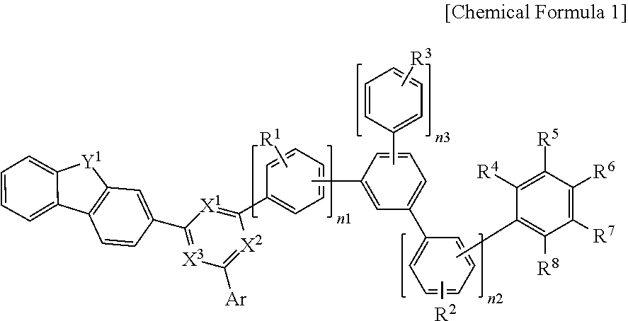
1. A compound for an organic optoelectronic device, the compound being represented by Chemical Formula 1: ##STR00115## wherein, in Chemical Formula 1, X.sup.1 to X.sup.3 are independently N or CR.sup.a, at least two of X.sup.1 to X.sup.3 are N, Y.sup.1 is O or S, Ar is a substituted or unsubstituted C6 to C30 aryl group, R.sup.a and R.sup.1 to R.sup.3 are independently hydrogen, deuterium, a substituted or unsubstituted C1 to C10 alkyl group, a substituted or unsubstituted C6 to C30 aryl group, or a combination thereof, R.sup.4 to R.sup.8 are independently hydrogen, deuterium, a cyano group, a nitro group, a substituted or unsubstituted C1 to C10 alkyl group, a substituted or unsubstituted C6 to C30 aryl group, a substituted or unsubstituted pyridinyl group, a substituted or unsubstituted quinolinyl group, a substituted or unsubstituted isoquinolinyl group, a substituted or unsubstituted dibenzofuranyl group, a substituted or unsubstituted dibenzothiophenyl group, or a combination thereof, R.sup.4 to R.sup.8 are independently present or adjacent groups thereof are linked with each other to provide a substituted or unsubstituted aliphatic, aromatic, or heteroaromatic monocyclic ring or polycyclic ring, n1 to n3 are independently an integer of 0 to 2, in case of n1+n2+n3=0, adjacent groups of R.sup.4 to R.sup.8 are linked with each other to provide a substituted or unsubstituted aliphatic, aromatic, or heteroaromatic monocyclic ring or polycyclic ring, and the "substituted" refers to replacement of at least one hydrogen by deuterium, a C1 to C20 alkyl group, a C6 to C30 aryl group, a substituted or unsubstituted pyridinyl group, a substituted or unsubstituted quinolinyl group, a substituted or unsubstituted isoquinolinyl group, a substituted or unsubstituted dibenzofuranyl group, or a substituted or unsubstituted dibenzothiophenyl group.
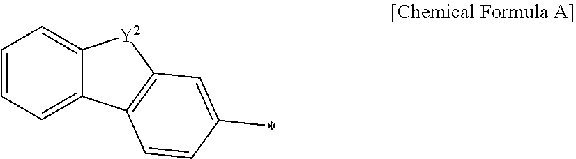
2. The compound for an organic optoelectronic device of claim 1, wherein adjacent groups of R.sup.4 to R.sup.8 are linked with each other to provide a heteroaromatic polycyclic ring represented by Chemical Formula A: ##STR00116## wherein, in Chemical Formula A, Y.sup.2 is O or S, and * is a linking point with a substituted or unsubstituted phenylene.
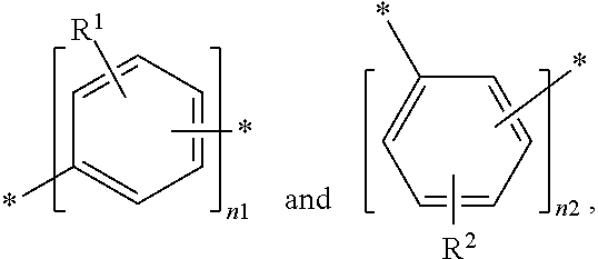
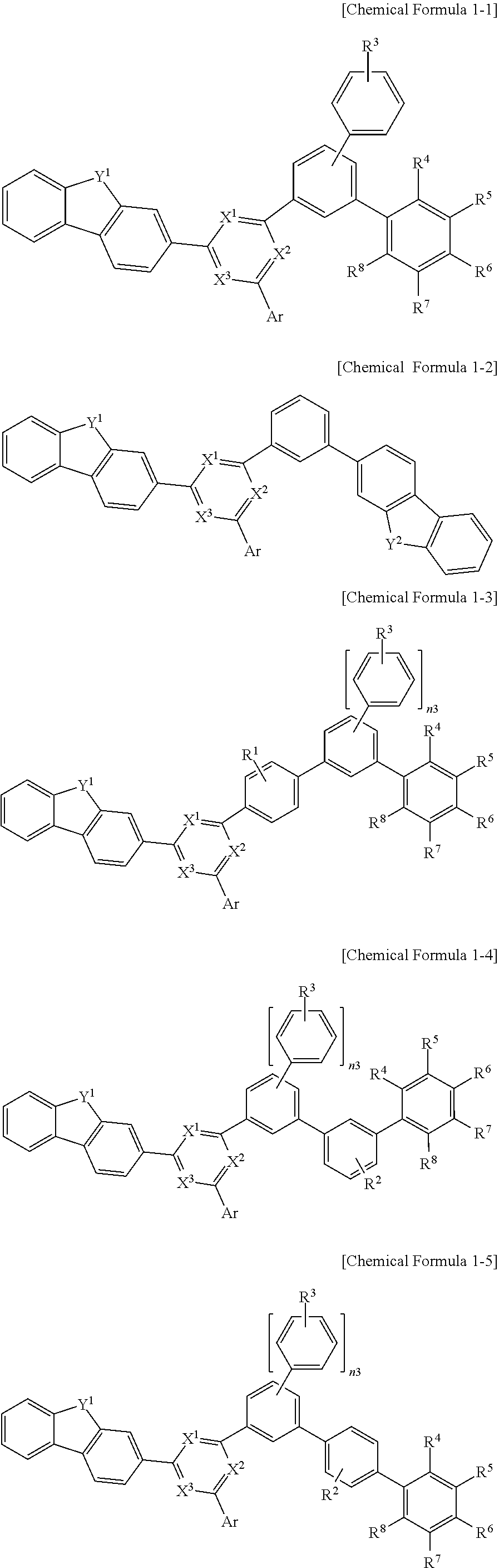
3. The compound for an organic optoelectronic device of claim 1, wherein the compound is represented by one of Chemical Formula 1-I, Chemical Formula 1-II, and Chemical Formula 1-III: ##STR00117## wherein, in Chemical Formula 1-I, Chemical Formula 1-II, and Chemical Formula 1-III, Y.sup.1 is O or S, Ar is a substituted or unsubstituted C6 to C30 aryl group, R.sup.1 to R.sup.3 are independently hydrogen, deuterium, a substituted or unsubstituted C1 to C10 alkyl group, a substituted or unsubstituted C6 to C30 aryl group, or a combination thereof, R.sup.4 to R.sup.8 are independently hydrogen, deuterium, a cyano group, a nitro group, a substituted or unsubstituted C1 to C10 alkyl group, a substituted or unsubstituted C6 to C30 aryl group, a substituted or unsubstituted pyridinyl group, a substituted or unsubstituted quinolinyl group, a substituted or unsubstituted isoquinolinyl group, a substituted or unsubstituted dibenzofuranyl group, a substituted or unsubstituted dibenzothiophenyl group, or a combination thereof, R.sup.4 to R.sup.8 are independently present or adjacent groups thereof are linked with each other to provide a substituted or unsubstituted aliphatic, aromatic, or heteroaromatic monocyclic ring or polycyclic ring, n1 to n3 are independently an integer of 0 to 2, and in case of n1+n2+n3=0, adjacent groups of R.sup.4 to R.sup.8 are linked with each other to provide a substituted or unsubstituted aliphatic, aromatic, or heteroaromatic monocyclic ring or polycyclic ring.
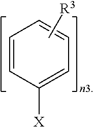
4. The compound for an organic optoelectronic device of claim 1, wherein the compound is represented by one of Chemical Formulae 1-1 to 1-6: ##STR00118## ##STR00119## wherein, in Chemical Formulae 1-1 to 1-5, X.sup.1 to X.sup.3 are independently N or CH, at least two of X.sup.1 to X.sup.3 are N, R.sup.1 to R.sup.3 are independently hydrogen, deuterium, a substituted or unsubstituted phenyl group, a substituted or unsubstituted biphenyl group, a substituted or unsubstituted naphthyl group, or a combination thereof, R.sup.4 to R.sup.8 are independently hydrogen, deuterium, a cyano group, a nitro group, a substituted or unsubstituted phenyl group, a substituted or unsubstituted biphenyl group, a dibenzofuranyl group, a dibenzothiophenyl group, or a combination thereof, and R.sup.4 to R.sup.8 are independently present or adjacent groups thereof are linked with each other to provide a heteroaromatic polycyclic ring represented by Chemical Formula A, ##STR00120## Y.sup.1 and Y.sup.2 are independently O or S, Ar is a substituted or unsubstituted phenyl group, a substituted or unsubstituted biphenyl group, a substituted or unsubstituted terphenyl group, a substituted or unsubstituted naphthyl group, a substituted or unsubstituted anthracenyl group, a substituted or unsubstituted phenanthrenyl group, a substituted or unsubstituted triphenylenyl group, a substituted or unsubstituted fluorenyl group, or a combination thereof, n3 is an integer of 0 or 1, and * is a linking point with a substituted or unsubstituted phenylene.
5. The compound for an organic optoelectronic device of claim 1, wherein the R.sup.1 to R.sup.3 are independently hydrogen, deuterium, or a substituted or unsubstituted phenyl group, R.sup.4 to R.sup.8 are independently hydrogen, deuterium, a substituted or unsubstituted phenyl group, or a substituted or unsubstituted biphenyl group, and R.sup.4 to R.sup.8 are independently present or adjacent groups thereof are linked with each other to provide a heteroaromatic polycyclic ring represented by Chemical Formula A, ##STR00121## Y.sup.2 is O or S, Ar is a substituted or unsubstituted phenyl group, a substituted or unsubstituted biphenyl group, a substituted or unsubstituted terphenyl group, or a substituted or unsubstituted naphthyl group.
6. The compound for an organic optoelectronic device of claim 1, wherein the compound is selected from compounds of Group 1: ##STR00122## ##STR00123## ##STR00124## ##STR00125## ##STR00126## ##STR00127## ##STR00128## ##STR00129## ##STR00130## ##STR00131## ##STR00132## ##STR00133## ##STR00134## ##STR00135## ##STR00136## ##STR00137## ##STR00138## ##STR00139## ##STR00140## ##STR00141## ##STR00142## ##STR00143## ##STR00144## ##STR00145## ##STR00146## ##STR00147## ##STR00148##
7. A composition for an organic optoelectronic device, comprising the compound for an organic optoelectronic device of claim 1; and a second compound for an organic optoelectronic device represented by Chemical Formula 2: ##STR00149## wherein, in Chemical Formula 2, L.sup.1 and L.sup.2 are independently a single bond, a substituted or unsubstituted C6 to C30 arylene group, a substituted or unsubstituted C2 to C30 heteroarylene group, or a combination thereof, Z.sup.1 and Z.sup.2 are independently a substituted or unsubstituted C6 to C30 aryl group, a substituted or unsubstituted C2 to C30 heterocyclic group, or a combination thereof, R.sup.9 to R.sup.14 are independently hydrogen, deuterium, a substituted or unsubstituted C1 to C20 alkyl group, a substituted or unsubstituted C6 to C30 aryl group, a substituted or unsubstituted C2 to C30 heterocyclic group, or a combination thereof, and m is an integer of 0 to 2; wherein the "substituted" refers to replacement of at least one hydrogen by deuterium, a C to C4 alkyl group, a C6 to C18 aryl group, or a C2 to C30 heteroaryl group.
8. The composition for an organic optoelectronic device of claim 7, wherein Z.sup.1 and Z.sup.2 of Chemical Formula 2 are independently a substituted or unsubstituted phenyl group, a substituted or unsubstituted biphenyl group, a substituted or unsubstituted terphenyl group, a substituted or unsubstituted naphthyl group, a substituted or unsubstituted anthracenyl group, a substituted or unsubstituted triphenylenyl group, a substituted or unsubstituted pyridinyl group, a substituted or unsubstituted pyrimidinyl group, a substituted or unsubstituted triazinyl group, a substituted or unsubstituted quinolinyl group, a substituted or unsubstituted isoquinolinyl group, a substituted or unsubstituted quinazolyl group, a substituted or unsubstituted isoquinazolyl group, a substituted or unsubstituted dibenzothiophenyl group, a substituted or unsubstituted dibenzofuranyl group, a substituted or unsubstituted carbazolyl group, a substituted or unsubstituted fluorenyl group, or a combination thereof.
9. The composition for an organic optoelectronic device of claim 7, wherein Chemical Formula 2 is one of structures of Group I, and *-L.sup.1-Z.sup.1 and *-L.sup.2-Z.sup.2 is one of substituents of Group II: ##STR00150## ##STR00151## ##STR00152## ##STR00153## ##STR00154## ##STR00155## ##STR00156## ##STR00157## ##STR00158## wherein, in Groups I and II, * is a linking point.
10. The composition for an organic optoelectronic device of claim 9, wherein Chemical Formula 2 is represented by Chemical Formula C-8 or Chemical Formula C-17 of Group I, and *-L.sup.1-Z.sup.1 and *-L.sup.2-Z.sup.2 is selected from B-1, B-2, B-3, and B-16 of Group II.
11. An organic optoelectronic device comprising an anode and a cathode facing each other, and at least one organic layer disposed between the anode and the cathode, wherein the organic layer includes the compound for an organic optoelectronic device of claim 1.
12. The organic optoelectronic device of claim 11, wherein the organic layer includes a light-emitting layer, and the light-emitting layer includes the compound for an organic optoelectronic device.
13. The organic optoelectronic device of claim 12, wherein the compound for an organic optoelectronic device is included as a host of the light-emitting layer.
14. The organic optoelectronic device of claim 12, wherein the organic layer further includes at least one auxiliary layer selected from a hole injection layer, a hole transport layer, an electron blocking layer, an electron transport layer, an electron injection layer, and a hole blocking layer, the auxiliary layer further includes an electron transport auxiliary layer that is adjacent to the light-emitting layer, and the electron transport auxiliary layer includes the compound for an organic optoelectronic device.
15. A display device comprising the organic optoelectronic device of claim 11.
16. An organic optoelectronic device comprising an anode and a cathode facing each other, and at least one organic layer disposed between the anode and the cathode, wherein the organic layer includes the composition for an organic optoelectronic device of claim 7.
17. A display device comprising the organic optoelectronic device of claim 16.
Description
TECHNICAL FIELD
[0001] A compound for an organic optoelectronic device, a composition for an organic optoelectronic device, an organic optoelectronic device, and a display device are disclosed.
BACKGROUND ART
[0002] An organic optoelectronic device (organic optoelectronic diode) is a device that converts electrical energy into photoenergy, and vice versa.
[0003] An organic optoelectronic device may be classified as follows in accordance with its driving principles. One is a photoelectric device where excitons are generated by photoenergy, separated into electrons and holes, and are transferred to different electrodes to generate electrical energy, and the other is a light emitting device where a voltage or a current is supplied to an electrode to generate photoenergy from electrical energy.
[0004] Examples of an organic optoelectronic device may be an organic photoelectric device, an organic light emitting diode, an organic solar cell, and an organic photo conductor drum.
[0005] Of these, an organic light emitting diode (OLED) has recently drawn attention due to an increase in demand for flat panel displays. The organic light emitting diode is a device converting electrical energy into light by applying current to an organic light emitting material, and has a structure in which an organic layer is disposed between an anode and a cathode. Herein, the organic layer may include a light-emitting layer and optionally an auxiliary layer, and the auxiliary layer may be, for example at least one selected from a hole injection layer, a hole transport layer, an electron blocking layer, an electron transport layer, an electron injection layer, and a hole blocking layer for improving efficiency and stability of an organic light emitting diode.
[0006] Performance of an organic light emitting diode may be affected by characteristics of the organic layer, and among them, may be mainly affected by characteristics of an organic material of the organic layer.
[0007] Particularly, development for an organic material being capable of increasing hole and electron mobility and simultaneously increasing electrochemical stability is needed so that the organic light emitting diode may be applied to a large-size flat panel display.
DISCLOSURE
Technical Problem
[0008] An embodiment provides a composition for an organic optoelectronic device capable of realizing an organic optoelectronic device having high efficiency and a long life-span.
[0009] Another embodiment provides a composition for an organic optoelectronic device including the compound for an organic optoelectronic device.
[0010] Yet another embodiment provides an organic optoelectronic device including the compound.
[0011] Still another embodiment provides a display device including the organic optoelectronic device.
Technical Solution
[0012] According to an embodiment, a compound represented by Chemical Formula 1 for an organic optoelectronic device is provided.
##STR00001##
[0013] In Chemical Formula 1,
[0014] X.sup.1 to X.sup.3 are independently N or CR.sup.a,
[0015] at least two of X.sup.1 to X.sup.3 are N,
[0016] Y.sup.1 is O or S,
[0017] Ar is a substituted or unsubstituted C6 to C30 aryl group,
[0018] R.sup.a and R.sup.1 to R.sup.3 are independently hydrogen, deuterium, a substituted or unsubstituted C1 to C10 alkyl group, a substituted or unsubstituted C6 to C30 aryl group, or a combination thereof,
[0019] R.sup.4 to R.sup.8 are independently hydrogen, deuterium, a cyano group, a nitro group, a substituted or unsubstituted C1 to C10 alkyl group, a substituted or unsubstituted C6 to C30 aryl group, a substituted or unsubstituted pyridinyl group, a substituted or unsubstituted quinolinyl group, a substituted or unsubstituted isoquinolinyl group, a substituted or unsubstituted dibenzofuranyl group, a substituted or unsubstituted dibenzothiophenyl group, or a combination thereof,
[0020] R.sup.4 to R.sup.8 are independently present or adjacent groups thereof are linked with each other to provide a substituted or unsubstituted aliphatic, aromatic, or heteroaromatic monocyclic ring or polycyclic ring and,
[0021] n1 to n3 are independently an integer of 0 to 2,
[0022] in case of n1+n2+n3=0, adjacent groups of R.sup.4 to R.sup.8 are linked with each other to provide a substituted or unsubstituted aliphatic, aromatic, or heteroaromatic monocyclic ring or polycyclic ring, and
[0023] the "substituted" refers to replacement of at least one hydrogen by deuterium, a C1 to C20 alkyl group, a C6 to C30 aryl group, a substituted or unsubstituted pyridinyl group, a substituted or unsubstituted quinolinyl group, a substituted or unsubstituted isoquinolinyl group, a substituted or unsubstituted dibenzofuranyl group, or a substituted or unsubstituted dibenzothiophenyl group.
[0024] According to another embodiment, a composition for an organic optoelectronic device includes the above compound for an organic optoelectronic device; and a second compound for an organic optoelectronic device represented by Chemical Formula 2.
##STR00002##
[0025] In Chemical Formula 2,
[0026] L.sup.1 and L.sup.2 are independently a single bond, a substituted or unsubstituted C6 to C30 arylene group, a substituted or unsubstituted C2 to C30 heteroarylene group, or a combination thereof,
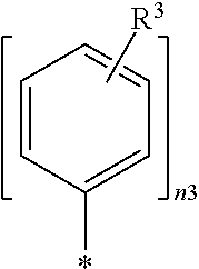
[0027] Z.sup.1 and Z.sup.2 are independently a substituted or unsubstituted C6 to C30 aryl group, a substituted or unsubstituted C2 to C30 heterocyclic group, or a combination thereof,
[0028] R.sup.9 to R.sup.14 are independently hydrogen, deuterium, a substituted or unsubstituted C1 to C20 alkyl group, a substituted or unsubstituted C6 to C30 aryl group, a substituted or unsubstituted C2 to C30 heterocyclic group, or a combination thereof, and
[0029] m is an integer of 0 to 2;
[0030] wherein the "substituted" refers to replacement of at least one hydrogen by deuterium, a C1 to C4 alkyl group, a C6 to C18 aryl group, or a C2 to C30 heteroaryl group.
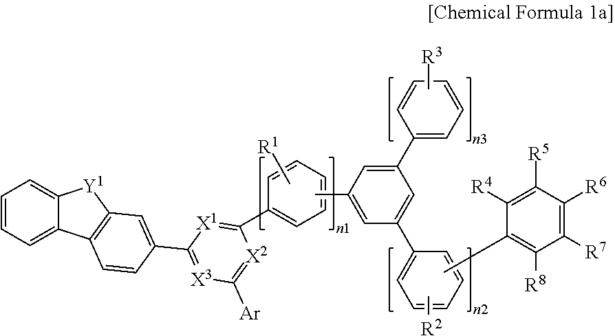
[0031] According to another embodiment, an organic optoelectronic device includes an anode and a cathode facing each other and at least one organic layer disposed between the anode and the cathode, wherein the organic layer includes the compound for an organic optoelectronic device, or the composition for an organic optoelectronic device.
[0032] According to another embodiment, a display device including the organic optoelectronic device is provided.
Advantageous Effects
[0033] An organic optoelectronic device having high efficiency and a long life-span may be realized.
DESCRIPTION OF THE DRAWINGS
[0034] FIGS. 1 and 2 are cross-sectional views showing organic light emitting diodes according embodiments.
DESCRIPTION OF SYMBOLS
[0035] 100, 200: organic light emitting diode [0036] 105: organic layer [0037] 110: cathode [0038] 120: anode [0039] 130: light-emitting layer [0040] 140: hole auxiliary layer
MODE FOR INVENTION
[0041] Hereinafter, embodiments of the present invention are described in detail. However, these embodiments are exemplary, the present invention is not limited thereto and the present invention is defined by the scope of claims.
[0042] As used herein, when a definition is not otherwise provided, the "substituted" refers to replacement of at least one hydrogen of a substituent or a compound by deuterium, a halogen, a hydroxyl group, an amino group, a substituted or unsubstituted C1 to C30 amine group, a nitro group, a substituted or unsubstituted C1 to C40 silyl group, a C1 to C30 alkyl group, a C1 to 010 alkylsilyl group, a C6 to C30 arylsilyl group, a C3 to C30 cycloalkyl group, a C3 to C30 heterocycloalkyl group, a C6 to C30 aryl group, a C2 to C30 heteroaryl group, a C1 to C20 alkoxy group, a fluoro group, a C1 to 010 trifluoroalkyl group, a cyano group, or a combination thereof.
[0043] In one example of the present invention, the "substituted" refers to replacement of at least one hydrogen of a substituent or a compound by deuterium, a C1 to C20 alkyl group, a C6 to C30 aryl group, a substituted or unsubstituted pyridinyl group, a substituted or unsubstituted quinolinyl group, a substituted or unsubstituted isoquinolinyl group, a substituted or unsubstituted dibenzofuranyl group, or a substituted or unsubstituted dibenzothiophenyl group.
[0044] As used herein, when a definition is not otherwise provided, "hetero" refers to one including one to three heteroatoms selected from N, O, S, P, and Si, and remaining carbons in one functional group.
[0045] As used herein, when a definition is not otherwise provided, "alkyl group" refers to an aliphatic hydrocarbon group. The alkyl group may be "a saturated alkyl group" without any double bond or triple bond.
[0046] The alkyl group may be a C1 to C30 alkyl group. More specifically, the alkyl group may be a C1 to C20 alkyl group or a C1 to 010 alkyl group. For example, a C1 to C4 alkyl group may have one to four carbon atoms in the alkyl chain, and may be selected from methyl, ethyl, propyl, iso-propyl, n-butyl, iso-butyl, sec-butyl, and t-butyl.
[0047] Specific examples of the alkyl group may be a methyl group, an ethyl group, a propyl group, an isopropyl group, a butyl group, an isobutyl group, a t-butyl group, a pentyl group, a hexyl group, a cyclopropyl group, a cyclobutyl group, a cyclopentyl group, a cyclohexyl group, and the like.
[0048] As used herein, an "aryl group" refers to a group including at least one hydrocarbon aromatic moiety, and
[0049] all the elements of the hydrocarbon aromatic moiety have p-orbitals which form conjugation, for example a phenyl group, a naphthyl group, and the like,
[0050] two or more hydrocarbon aromatic moieties may be linked by a sigma bond and may be, for example a biphenyl group, a terphenyl group, a quarterphenyl group, and the like, and
[0051] two or more hydrocarbon aromatic moieties are fused directly or indirectly to provide a non-aromatic fused ring. For example, it may be a fluorenyl group.
[0052] The aryl group may include a monocyclic, polycyclic or fused ring polycyclic (i.e., rings sharing adjacent pairs of carbon atoms) functional group.
[0053] As used herein, "heterocyclic group" is a generic concept of a heteroaryl group, and may include at least one heteroatom selected from N, O, S, P, and Si instead of carbon (C) in a cyclic compound such as an aryl group, a cycloalkyl group, a fused ring thereof, or a combination thereof. When the heterocyclic group is a fused ring, the entire ring or each ring of the heterocyclic group may include one or more heteroatoms.
[0054] For example, a "heteroaryl group" may refer to an aryl group including at least one heteroatom selected from N, O, S, P, and Si. Two or more heteroaryl groups are linked by a sigma bond directly, or when the heteroaryl group includes two or more rings, the two or more rings may be fused. When the heteroaryl group is a fused ring, each ring may include one to three heteroatoms.
[0055] Specific examples of the heterocyclic group may be a pyridinyl group, a pyrimidinyl group, a pyrazinyl group, a pyridazinyl group, a triazinyl group, a quinolinyl group, an isoquinolinyl group, and the like.
[0056] More specifically, the substituted or unsubstituted C6 to C30 aryl group and/or the substituted or unsubstituted C2 to C30 heterocyclic group may be a substituted or unsubstituted phenyl group, a substituted or unsubstituted naphthyl group, a substituted or unsubstituted anthracenyl group, a substituted or unsubstituted phenanthrenyl group, a substituted or unsubstituted naphthacenyl group, a substituted or unsubstituted pyrenyl group, a substituted or unsubstituted biphenyl group, a substituted or unsubstituted p-terphenyl group, a substituted or unsubstituted m-terphenyl group, a substituted or unsubstituted o-terphenyl group, a substituted or unsubstituted chrysenyl group, a substituted or unsubstituted triphenylenyl group, a substituted or unsubstituted perylenyl group, a substituted or unsubstituted fluorenyl group, a substituted or unsubstituted indenyl group, a substituted or unsubstituted furanyl group, a substituted or unsubstituted thiophenyl group, a substituted or unsubstituted pyrrolyl group, a substituted or unsubstituted pyrazolyl group, a substituted or unsubstituted imidazolyl group, a substituted or unsubstituted triazolyl group, a substituted or unsubstituted oxazolyl group, a substituted or unsubstituted thiazolyl group, a substituted or unsubstituted oxadiazolyl group, a substituted or unsubstituted thiadiazolyl group, a substituted or unsubstituted pyridyl group, a substituted or unsubstituted pyrimidinyl group, a substituted or unsubstituted pyrazinyl group, a substituted or unsubstituted triazinyl group, a substituted or unsubstituted benzofuranyl group, a substituted or unsubstituted benzothiophenyl group, a substituted or unsubstituted benzimidazolyl group, a substituted or unsubstituted indolyl group, a substituted or unsubstituted quinolinyl group, a substituted or unsubstituted isoquinolinyl group, a substituted or unsubstituted quinazolinyl group, a substituted or unsubstituted quinoxalinyl group, a substituted or unsubstituted naphthyridinyl group, a substituted or unsubstituted benzoxazinyl group, a substituted or unsubstituted benzthiazinyl group, a substituted or unsubstituted acridinyl group, a substituted or unsubstituted phenazinyl group, a substituted or unsubstituted phenothiazinyl group, a substituted or unsubstituted phenoxazinyl group, a substituted or unsubstituted dibenzofuranyl group, or a substituted or unsubstituted dibenzothiophenyl group, or a combination thereof, but are not limited thereto.
[0057] In the present specification, hole characteristics refer to an ability to donate an electron to form a hole when an electric field is applied, and that a hole formed in the anode may be easily injected into a light-emitting layer, and a hole formed in a light-emitting layer may be easily transported into an anode and transported in a light-emitting layer due to conductive characteristics according to a highest occupied molecular orbital (HOMO) level.
[0058] In addition, electron characteristics refer to an ability to accept an electron when an electric field is applied and that an electron formed in a cathode may be easily injected into a light-emitting layer, and an electron formed in a light-emitting layer may be easily transported into a cathode and transported in a light-emitting layer due to conductive characteristics according to a lowest unoccupied molecular orbital (LUMO) level. For example, ET core means a core which has electron characteristics.
[0059] Hereinafter, a compound for an organic optoelectronic device according to an embodiment is described.
[0060] A compound for an organic optoelectronic device according to an embodiment is represented by Chemical Formula 1.
##STR00003##
[0061] In Chemical Formula 1,
[0062] X.sup.1 to X.sup.3 are independently N or CR.sup.a,
[0063] at least two of X.sup.1 to X.sup.3 are N,
[0064] Y.sup.1 is O or S,
[0065] Ar is a substituted or unsubstituted C6 to C30 aryl group,
[0066] R.sup.a and R.sup.1 to R.sup.3 are independently hydrogen, deuterium, a substituted or unsubstituted C1 to 010 alkyl group, a substituted or unsubstituted C6 to C30 aryl group, or a combination thereof,
[0067] R.sup.4 to R.sup.8 are independently hydrogen, deuterium, a cyano group, a nitro group, a substituted or unsubstituted C1 to 010 alkyl group, a substituted or unsubstituted C6 to C30 aryl group, a substituted or unsubstituted pyridinyl group, a substituted or unsubstituted quinolinyl group, a substituted or unsubstituted isoquinolinyl group, a substituted or unsubstituted dibenzofuranyl group, a substituted or unsubstituted dibenzothiophenyl group, or a combination thereof,
[0068] R.sup.4 to R.sup.8 are independently present or adjacent groups thereof are linked with each other to provide a substituted or unsubstituted aliphatic, aromatic, or heteroaromatic monocyclic ring or polycyclic ring,
[0069] n1 to n3 are independently an integer of 0 to 2,
[0070] in case of n1+n2+n3=0, adjacent groups of R.sup.4 to R.sup.8 are linked with each other to provide a substituted or unsubstituted aliphatic, aromatic, or heteroaromatic monocyclic ring or polycyclic ring, and
[0071] the "substituted" refers to replacement of at least one hydrogen by deuterium, a C1 to C20 alkyl group, a C6 to C30 aryl group, a substituted or unsubstituted pyridinyl group, a substituted or unsubstituted quinolinyl group, a substituted or unsubstituted isoquinolinyl group, a substituted or unsubstituted dibenzofuranyl group, or a substituted or unsubstituted dibenzothiophenyl group. In an embodiment of the present invention, the "substituted" refers to replacement of at least one hydrogen by deuterium, C1 to C5 alkyl group, a C6 to C18 aryl group, a substituted or unsubstituted pyridinyl group, a substituted or unsubstituted quinolinyl group, a substituted or unsubstituted isoquinolinyl group, a substituted or unsubstituted dibenzofuranyl group, or a substituted or unsubstituted dibenzothiophenyl group. In a specific example embodiment of the present invention, the "substituted" refers to replacement of at least one hydrogen by deuterium, a phenyl group, a meta-biphenyl group, a para-biphenyl group, 3-dibenzofuranyl group, or a 3-dibenzothiophenyl group.
[0072] A compound for an organic optoelectronic device according to the present invention includes an ET core including an N-containing 6-membered ring that includes a substituent directly linked with dibenzofuran or dibenzothiophene at a position No. 3 without a linking group, and thereby a LUMO energy band is effectively expanded, planarity of a molecular structure is increased, and the compound may become a structure capable of accepting electrons when an electric field is applied, and accordingly an organic optoelectronic device including the compound for an organic optoelectronic device may exhibit a lowered driving voltage. Such a LUMO expansion and ring fusion increase stability for electrons of the ET core and life-span of a device is effectively improved.
[0073] In addition, interactions with adjacent molecules may be suppressed and crystallization is decreased due to steric hindrance characteristics by at least one meta-bound arylene and accordingly efficiency and life-span characteristics of an organic optoelectronic device including the compound for an organic optoelectronic device may be improved.
[0074] A kinked moiety such as the meta-bound arylene increases a glass transition temperature (Tg) of a compound and stability of a compound may be increased and degradation may be suppressed when it is applied to a device.
[0075] In the present invention, "adjacent groups thereof are linked with each other" in definition of R.sup.4 to R.sup.8 refers to fusion of a phenyl group linked with R.sup.4 to R.sup.8 with two substituents of R.sup.4 to R.sup.8 to provide a substituted or unsubstituted aliphatic, aromatic, or heteroaromatic monocyclic ring or polycyclic ring. For example, each of R.sup.4 and R.sup.5, R.sup.5 and R.sup.6, R.sup.6 and R.sup.7, and R.sup.7 and R.sup.8 may form a heteroaromatic polycyclic ring with the phenyl group. Herein examples of the heteroaromatic polycyclic ring may be a substituted or unsubstituted dibenzofuranyl group, a substituted or unsubstituted dibenzothiophenyl group, and the like, and for example adjacent groups of R.sup.4 to R.sup.8 may be linked with the phenyl group to provide a heteroaromatic polycyclic ring represented by Chemical Formula A.
##STR00004##
[0076] In Chemical Formula A, Y.sup.2 is O or S, and * is a linking point with a substituted or unsubstituted phenylene.
[0077] Specific examples of a compound where adjacent groups of R.sup.4 to R.sup.8 are linked with each other to provide a heteroaromatic polycyclic ring may be "Compound B-10" of the following specific compounds of the present invention.
[0078] In an example embodiment of the present invention, an ET core consisting of X.sup.1 to X.sup.3 may be pyrimidine or triazine and may be for example represented by Chemical Formula 1-I, Chemical Formula 1-II, or Chemical Formula 1-III. More specifically, it may be represented by Chemical Formula 1-I or Chemical Formula 1-II.
##STR00005##
[0079] In Chemical Formula 1-I, Chemical Formula 1-II, and Chemical Formula 1-III, Y.sup.1, Ar, R.sup.1 to R.sup.8, and n1 to n3 are the same as described above.
[0080] In an example embodiment of the present invention, n1 may be an integer ranging from 0 to 2 and n2 and n3 may independently be an integer of 0 or 1. When n1 is 2, each R.sup.1 may be the same or different. Specifically, n1 may be an integer of 0 or 1.
[0081] In another example embodiment of the present invention, n2 may be an integer ranging from 0 to 2 and n1 and n3 may independently be an integer of 0 or 1. When n2 is 2, each R.sup.2 may be the same or different. Specifically, n2 may be an integer of 0 or 1.
[0082] In another example embodiment of the present invention, n3 may be an integer ranging from 0 to 2 and n1 and n2 may independently be an integer of 0 or 1. When n3 is 2, each R.sup.3 may be the same or different. Specifically, n3 may be an integer of 0 or 1.
[0083] In an example embodiment of the present invention, the n1 to n3 may independently be in integer of 0 or 1, for example n1 and n4 may be 0 or at least one of n1 and n2 may be 1.
[0084] Chemical Formula 1 may be for example represented by one of Chemical Formulae 1-1 to 1-5 according to presences of a linking group represented by
##STR00006##
and a substituent represented by
##STR00007##
Herein, the linking group may be linked by a meta bond or a para bond.
##STR00008##
[0085] In Chemical Formulae 1-1 to 1-5, R.sup.1 to R.sup.8, Y.sup.1 and Y.sup.2, Ar, and n3 are the same as above,
[0086] X.sup.1 to X.sup.3 are independently N or CH and at least two of X.sup.1 to X.sup.3 are N.
[0087] In an example embodiment of the present invention, Chemical Formula 1 may be represented by Chemical Formula 1-1, Chemical Formula 1-3, Chemical Formula 1-4, or Chemical Formula 1-5, and may be for example represented by Chemical Formula 1-4.
[0088] Particularly, when the substituent represented by
##STR00009##
is present, that is n3 is 1 or 2, Chemical Formula 1 may be represented by Chemical Formula 1a including a kinked terphenyl group.
##STR00010##
[0089] In addition, Chemical Formula 1 may be for example represented by one of Chemical Formula 1-1a, Chemical Formula 1-3a, Chemical Formula 1-4a, and Chemical Formula 1-5a according to presences of a linking group represented by
##STR00011##
and a substituent represented by
##STR00012##
##STR00013##
[0090] Y.sup.1, X.sup.1 to X.sup.3, Ar, and R.sup.1 to R.sup.8 are the same as above and n3 is an integer of 1 or 2.
[0091] When the kinked terphenyl group is included, a glass transition temperature (Tg) may be increased effectively, and a low molecular weight compound having a high glass transition temperature (Tg) may be designed and thereby thermal characteristics may be ensured and stability and the like may be ensured.
[0092] The glass transition temperature (Tg) may have a relation with thermal stability of a compound and a device including the same. That is, when a compound for an organic optoelectronic device having a high glass transition temperature (Tg) is applied to an organic light emitting diode in a form of a thin film, degradation by temperature may be prevented and an organic compound and life-span characteristics of a device may be ensured in subsequent processes after deposition of the compound for an organic optoelectronic device.
[0093] In an example embodiment of the present invention, Ar may be a substituted or unsubstituted phenyl group, a substituted or unsubstituted biphenyl group, a substituted or unsubstituted terphenyl group, a substituted or unsubstituted naphthyl group, a substituted or unsubstituted anthracenyl group, a substituted or unsubstituted phenanthrenyl group, a substituted or unsubstituted triphenylenyl group, a substituted or unsubstituted fluorenyl group, or a combination thereof,
[0094] for example, a phenyl group, a m-biphenyl group, or a p-biphenyl group.
[0095] In an example embodiment of the present invention, R.sup.a and R.sup.1 to R.sup.3 may independently be hydrogen, deuterium, a substituted or unsubstituted C1 to C10 alkyl group, a substituted or unsubstituted C6 to C30 aryl group, or a combination thereof, and specifically, hydrogen, deuterium, or a substituted or unsubstituted C6 to C18 aryl group, for example, hydrogen, or a phenyl group. In a specific example embodiment, R.sup.a may be hydrogen and R.sup.1 to R.sup.3 may be hydrogen or a phenyl group.
[0096] In an example embodiment of the present invention, R.sup.4 to R.sup.8 may be independently hydrogen, deuterium, a cyano group, a nitro group, a substituted or unsubstituted C1 to 010 alkyl group, a substituted or unsubstituted C6 to C30 aryl group, a substituted or unsubstituted pyridinyl group, a substituted or unsubstituted quinolinyl group, a substituted or unsubstituted isoquinolinyl group, a substituted or unsubstituted dibenzofuranyl group, a substituted or unsubstituted dibenzothiophenyl group, or a combination thereof, and R.sup.4 to R.sup.8 may independently be present or adjacent groups thereof may be linked with each other to provide a substituted or unsubstituted aliphatic, aromatic, or heteroaromatic monocyclic ring or polycyclic ring
[0097] R.sup.4 to R.sup.8 may be independently present or adjacent groups thereof are linked with each other to provide a substituted or unsubstituted aliphatic, aromatic, or heteroaromatic monocyclic ring or polycyclic ring and examples of the heteroaromatic polycyclic ring may be a dibenzofuranyl group or a dibenzothiophenyl group.
[0098] For example, all R.sup.4 to R.sup.8 may be hydrogen or at least one of R.sup.5 to R.sup.7 may be a phenyl group, a biphenyl group, a dibenzofuranyl group, or a dibenzothiophenyl group and the rest may be hydrogen.
[0099] In addition, R.sup.5 and R.sup.6 or R.sup.6 and R.sup.7 are linked with each other to provide a heteroaromatic polycyclic ring represented by Chemical Formula A.
[0100] The compound for an organic optoelectronic device represented by Chemical Formula 1 may be for example selected from compounds of Group 1, but is not limited thereto.
##STR00014## ##STR00015## ##STR00016## ##STR00017## ##STR00018## ##STR00019## ##STR00020## ##STR00021## ##STR00022## ##STR00023## ##STR00024## ##STR00025## ##STR00026## ##STR00027## ##STR00028## ##STR00029## ##STR00030## ##STR00031## ##STR00032## ##STR00033## ##STR00034## ##STR00035## ##STR00036## ##STR00037## ##STR00038## ##STR00039## ##STR00040##
[0101] The first compound for an organic optoelectronic device may be applied to an organic optoelectronic device alone or with other compounds for an organic optoelectronic device. When the compound for an organic optoelectronic device is used with other compounds for an organic optoelectronic device, they may be applied in a form of a composition.
[0102] Hereinafter, one example of a composition for an organic optoelectronic device including the first compound for an organic optoelectronic device is described.
[0103] A composition for an organic optoelectronic device according to another embodiment of the present invention includes the first compound for an organic optoelectronic device; and a second compound for an organic optoelectronic device represented by Chemical Formula 2.
##STR00041##
[0104] In Chemical Formula 2,
[0105] L.sup.1 and L.sup.2 are independently a single bond, a substituted or unsubstituted C6 to C30 arylene group, a substituted or unsubstituted C2 to C30 heteroarylene group, or a combination thereof,
[0106] Z.sup.1 and Z.sup.2 are independently a substituted or unsubstituted C6 to C30 aryl group, a substituted or unsubstituted C2 to C30 heterocyclic group, or a combination thereof,
[0107] R.sup.9 to R.sup.14 are independently hydrogen, deuterium, a substituted or unsubstituted C1 to C20 alkyl group, a substituted or unsubstituted C6 to C30 aryl group, a substituted or unsubstituted C2 to C30 heterocyclic group, or a combination thereof, and
[0108] m is an integer of 0 to 2;
[0109] wherein the "substituted" refers to replacement of at least one hydrogen by deuterium, a C1 to C4 alkyl group, a C6 to C18 aryl group, or a C2 to C30 heteroaryl group. In a specific example embodiment of the present invention, the "substituted" refers to replacement of at least one hydrogen by deuterium, a phenyl group, an ortho-biphenyl group, a meta-biphenyl group, a para-biphenyl group, a terphenyl group, a naphthyl group, a dibenzofuranyl group, or a dibenzothiophenyl group.
[0110] In an example embodiment of the present invention, L.sup.1 and L.sup.2 of Chemical Formula 2 may independently be a single bond, or a substituted or unsubstituted C6 to C18 arylene group.
[0111] In an example embodiment of the present invention, Z.sup.1 and Z.sup.2 of Chemical Formula 2 may independently be a substituted or unsubstituted phenyl group, a substituted or unsubstituted biphenyl group, a substituted or unsubstituted terphenyl group, a substituted or unsubstituted naphthyl group, a substituted or unsubstituted anthracenyl group, a substituted or unsubstituted triphenylenyl group, a substituted or unsubstituted pyridinyl group, a substituted or unsubstituted pyrimidinyl group, a substituted or unsubstituted quinazolyl group, a substituted or unsubstituted isoquinazolyl group, a substituted or unsubstituted dibenzothiophenyl group, a substituted or unsubstituted dibenzofuranyl group, a substituted or unsubstituted triazinyl group, a substituted or unsubstituted quinolinyl group, a substituted or unsubstituted isoquinolinyl group, a substituted or unsubstituted carbazolyl group, a substituted or unsubstituted fluorenyl group, or a combination thereof.
[0112] Specifically, Z.sup.1 and Z.sup.2 of Chemical Formula 2 may independently be a substituted or unsubstituted phenyl group, a substituted or unsubstituted biphenyl group, a substituted or unsubstituted terphenyl group, a substituted or unsubstituted naphthyl group, a substituted or unsubstituted triphenylenyl group, a substituted or unsubstituted pyridinyl group, a substituted or unsubstituted pyrimidinyl group, a substituted or unsubstituted dibenzothiophenyl group, a substituted or unsubstituted dibenzofuranyl group, a substituted or unsubstituted carbazolyl group, a substituted or unsubstituted fluorenyl group, or a combination thereof, and may be for example a phenyl group, a biphenyl group, a dibenzofuranyl group, or a dibenzothiophenyl group.
[0113] In an example embodiment of the present invention, R.sup.9 to R.sup.14 of Chemical Formula 2 may independently be hydrogen, deuterium, or a substituted or unsubstituted C6 to C12 aryl group.
[0114] In an example embodiment of the present invention, m of Chemical Formula 2 may be 0 or 1.
[0115] In a specific example embodiment of the present invention, Chemical Formula 2 may be one of structures of Group I and *-L.sup.1-Z.sup.1 and *-L.sup.2-Z.sup.2 may be one of substituents of Group II.
##STR00042## ##STR00043## ##STR00044## ##STR00045## ##STR00046## ##STR00047## ##STR00048## ##STR00049## ##STR00050##
[0116] In Groups I and II, * is a linking point.
[0117] The second compound for an organic optoelectronic device represented by Chemical Formula 2 may be for example selected from compounds of Group 2.
##STR00051## ##STR00052## ##STR00053## ##STR00054## ##STR00055## ##STR00056## ##STR00057## ##STR00058## ##STR00059## ##STR00060## ##STR00061## ##STR00062## ##STR00063## ##STR00064## ##STR00065## ##STR00066## ##STR00067## ##STR00068## ##STR00069## ##STR00070## ##STR00071## ##STR00072## ##STR00073## ##STR00074## ##STR00075## ##STR00076## ##STR00077## ##STR00078## ##STR00079## ##STR00080## ##STR00081## ##STR00082## ##STR00083## ##STR00084## ##STR00085## ##STR00086## ##STR00087## ##STR00088## ##STR00089## ##STR00090## ##STR00091## ##STR00092## ##STR00093## ##STR00094## ##STR00095## ##STR00096##
[0118] The first compound (first host) and the second compound (second host) may variously be combined to provide various compositions.
[0119] A composition according to an example embodiment of the present invention includes a compound represented by Chemical Formula 1-1, Chemical Formula 1-3, Chemical Formula 1-4, or Chemical Formula 1-5 as a first host, and a compound represented by Chemical Formula C-8 or Chemical Formula C-17 of Group I as a second host.
[0120] In addition, a first host represented by Chemical Formula 1-I, Chemical Formula 1-II, or Chemical Formula 1-III and a second host represented by Chemical Formula C-8 or Chemical Formula C-17 of Group I may be included.
[0121] For example, *-L.sup.1-Z.sup.1 and *-L.sup.2-Z.sup.2 of Chemical Formula 2 may be selected from B-1, B-2, B-3, and B-16 of Group II.
[0122] The second compound for an organic optoelectronic device is used with the first compound for an organic optoelectronic device in a light-emitting layer, and thereby charge mobility and stability are increased and luminous efficiency and life-span characteristics are improved. In addition, a ratio between the second compound for an organic optoelectronic device and the first compound for an organic optoelectronic device is controlled and thereby charge mobility may be controlled.
[0123] For example, the first compound for an organic optoelectronic device and the second compound for an organic optoelectronic device may be included in a weight ratio of about 1:9 to 9:1, specifically 2:8 to 8:2, 3:7 to 7:3, 4:6 to 6:4, or 5:5, and for example the first compound for an organic optoelectronic device and the second compound for an organic optoelectronic device may be included in a weight ratio of 3:7. Within the ranges, efficiency and life-span may be improved simultaneously.
[0124] The composition may further include one or more organic compound in addition to the first compound for an organic optoelectronic device and the second compound for an organic optoelectronic device.
[0125] The compound for an organic optoelectronic device may further include a dopant. The dopant may be a red, green, or blue dopant.
[0126] The dopant is a material in small amount to cause light emission and may be generally a material such as a metal complex that emits light by multiple excitation into a triplet or more. The dopant may be for example an inorganic, organic, or organic/inorganic compound, and one or more kinds thereof may be used.
[0127] One example of the dopant may be a phosphorescent dopant and examples of the phosphorescent dopant may be an organometal compound including Ir, Pt, Os, Ti, Zr, Hf, Eu, Tb, Tm, Fe, Co, Ni, Ru, Rh, Pd, or a combination thereof. The phosphorescent dopant may be, for example a compound represented by Chemical Formula Z, but is not limited thereto.
L.sub.2MX [Chemical Formula Z]
[0128] In Chemical Formula Z, M is a metal, and L and X are the same or different, and are a ligand to form a complex compound with M.
[0129] The M may be for example, Ir, Pt, Os, Ti, Zr, Hf, Eu, Tb, Tm, Fe, Co, Ni, Ru, Rh, Pd, or a combination thereof and L and X may be for example a bidendate ligand.
[0130] Hereinafter, an organic optoelectronic device including the compound for an organic optoelectronic device or the composition for an organic optoelectronic device is described.
[0131] An organic optoelectronic device according to another embodiment includes an anode and a cathode facing each other and at least one organic layer disposed between the anode and the cathode, wherein the organic layer includes the compound for an organic optoelectronic device or the composition for an organic optoelectronic device.
[0132] For example, the organic layer may include a light-emitting layer and the light-emitting layer may include the compound for an organic optoelectronic device or the composition for an organic optoelectronic device.
[0133] Specifically, the compound for an organic optoelectronic device or the composition for an organic optoelectronic device may be included as a green host of the light-emitting layer.
[0134] In addition, the organic layer includes a light-emitting layer and at least one auxiliary layer selected from a hole injection layer, a hole transport layer, an electron blocking layer, an electron transport layer, an electron injection layer, and a hole blocking layer and the auxiliary layer may include the compound for an organic optoelectronic device or the composition for an organic optoelectronic device.
[0135] The auxiliary layer may further include an electron transport auxiliary layer that is adjacent to the light-emitting layer and the electron transport auxiliary layer may include the compound for an organic optoelectronic device, or the composition for an organic optoelectronic device.
[0136] In an example embodiment of the present invention, the compound for an organic optoelectronic device in the electron transport auxiliary layer may be represented by Chemical Formula 1-3.
[0137] The organic optoelectronic device may be any device to convert electrical energy into photoenergy and vice versa without particular limitation, and may be, for example an organic photoelectric diode, an organic light emitting diode, an organic solar cell, and an organic photo conductor drum.
[0138] Herein, an organic light emitting diode as one example of an organic optoelectronic device is described referring to drawings.
[0139] FIGS. 1 and 2 are cross-sectional views showing organic light emitting diodes according to embodiments.
[0140] Referring to FIG. 1, an organic light emitting diode 100 according to an embodiment includes an anode 120 and a cathode 110 facing each other and an organic layer 105 between the anode 120 and the cathode 110.
[0141] The anode 120 may be made of a conductor having a large work function to help hole injection, and may be for example a metal, a metal oxide and/or a conductive polymer. The anode 120 may be, for example a metal nickel, platinum, vanadium, chromium, copper, zinc, gold, and the like or an alloy thereof; metal oxide such as zinc oxide, indium oxide, indium tin oxide (ITO), indium zinc oxide (IZO), and the like; a combination of metal and oxide such as ZnO and Al or SnO.sub.2 and Sb; a conductive polymer such as poly(3-methylthiophene), poly(3,4-(ethylene-1,2-dioxy)thiophene) (PEDT), polypyrrole, and polyaniline, but is not limited thereto.
[0142] The cathode 110 may be made of a conductor having a small work function to help electron injection, and may be for example a metal, a metal oxide and/or a conductive polymer. The cathode 110 may be for example a metal or an alloy thereof such as magnesium, calcium, sodium, potassium, titanium, indium, yttrium, lithium, gadolinium, aluminum, silver, tin, lead, cesium, barium, and the like; a multi-layer structure material such as LiF/Al, LiO.sub.2/Al, LiF/Ca, LiF/Al and BaF.sub.2/Ca, but is not limited thereto.
[0143] The organic layer 105 includes a light-emitting layer 130 including the compound for an organic optoelectronic device.
[0144] FIG. 2 is a cross-sectional view of an organic light emitting diode according to another embodiment.
[0145] Referring to FIG. 2, an organic light emitting diode 200 further includes a hole auxiliary layer 140 in addition to the light-emitting layer 130. The hole auxiliary layer 140 may further increase hole injection and/or hole mobility and block electrons between the anode 120 and the light-emitting layer 130. The hole auxiliary layer 140 may be, for example a hole transport layer, a hole injection layer, and/or an electron blocking layer, and may include at least one layer.
[0146] The organic layer 105 of FIG. 1 or 2 may further include an electron injection layer, an electron transport layer, an electron transport auxiliary layer, a hole transport layer, a hole transport auxiliary layer, a hole injection layer, or a combination thereof even if they are not shown. The compound for an organic optoelectronic device of the present invention may be included in these organic layers. The organic light emitting diodes 100 and 200 may be manufactured by forming an anode or a cathode on a substrate, forming an organic layer using a dry film formation method such as a vacuum deposition method (evaporation), sputtering, plasma plating, and ion plating or a wet coating method such as spin coating, dipping, and flow coating, and forming a cathode or an anode thereon.
[0147] The organic light emitting diode may be applied to an organic light emitting diode display.
[0148] Hereinafter, the embodiments are illustrated in more detail with reference to examples. These examples, however, are not in any sense to be interpreted as limiting the scope of the invention.
[0149] Hereinafter, starting materials and reactants used in Examples and Synthesis Examples were purchased from Sigma-Aldrich Co., Ltd. or TCI Inc. as far as there is no particular comment or were synthesized by known methods.
(Preparation of Compound for Organic Optoelectronic Device)
[0150] The compound as one specific examples of the present invention was synthesized through the following steps.
(First Compound for Organic Optoelectronic Device)
Synthesis Example 1: Synthesis of Compound B-1
##STR00097##
[0151] a) Synthesis of Intermediate B-1-1
[0152] 2,4-dichloro-6-phenyltriazine (22.6 g, 100 mmol) was put in tetrahydrofuran (100 mL), toluene (100 mL), and distilled water (100 mL) in a 500 mL round-bottomed flask, 0.9 equivalents of dibenzofuran-3-boronic acid (CAS No: 395087-89-5), 0.03 equivalents of tetrakistriphenylphosphine palladium, and 2 equivalents of potassium carbonate were added, and the mixture was heated and refluxed under a under a nitrogen atmosphere. After 6 hours, a reaction solution was cooled down, an aqueous layer was removed and then an organic layer was dried under reduced pressure. Obtained solid was washed with water and hexane, and the solid was recrystallized with toluene (200 mL) to obtain 21.4 g (60% yield) of Intermediate B-1-1.
b) Synthesis of Compound B-1
[0153] The synthesized Intermediate B-1-1 (56.9 mmol) was put in tetrahydrofuran (200 mL) and distilled water (100 mL) in a 500 mL round-bottomed flask, and 1.1 equivalents of 3,5-diphenylbenzeneboronic acid (CAS No.: 128388-54-5), 0.03 equivalents of tetrakistriphenylphosphine palladium, and 2 equivalents of potassium carbonate were added, and the mixture was heated and refluxed under a under a nitrogen atmosphere. After 18 hours, a reaction solution was cooled, and a solid precipitated therein was filtered and washed with water (500 mL). The solid was recrystallized with monochlorobenzene (500 mL) to obtain Compound B-1.
[0154] LC/MS calculated for: C39H25N.sub.3O Exact Mass: 555.1998 found for 556.21 [M+H].
Synthesis Example 2: Synthesis of Compound B-7
##STR00098##
[0155] a) Synthesis of Intermediate B-7-1
[0156] Intermediate B-7-1 was synthesized according to the same method as b) of Synthesis Example 1 by using 1-bromo-3-chloro-5-phenylbenzene and 1.1 equivalents of biphenyl-4-boronic acid. Herein, a product was purified through a flash column using hexane instead of recrystallization.
b) Synthesis of Intermediate B-7-2
[0157] The synthesized intermediate B-7-1 30 g (88.02 mmol) was put in DMF (250 mL) in a 500 mL round-bottomed flask, 0.05 equivalents of dichlorodiphenyl phosphinoferrocene palladium, 1.2 equivalents of bispinacolato diboron, and 2 equivalents of potassium acetate were put, and heated and refluxed under a under a nitrogen atmosphere for 18 hours. A reaction solution was cooled down and was dripped in 1 L of water to capture a solid. The obtained solid was dissolved in boiling toluene and was treated with activated carbon, and then filtrate was concentrated after filtering with a silica gel filter. A concentrated solid was stirred with a small amount of hexane, and then the solid was filtered to obtain 28.5 g (a yield of 70%) of Intermediate B-7-2.
c) Synthesis of Compound B-7
[0158] Compound B-7 was synthesized according to the same method as b) of Synthesis Example 1 by using 1.0 equivalent of Intermediate B-7-2 and 1.0 equivalent of Intermediate B-1-1.
[0159] LC/MS calculated for: C45H29N3O Exact Mass: 627.2311 found for 628.22 [M+H].
Synthesis Example 3: Synthesis of Compound B-9
##STR00099##
[0160] a) Synthesis of Intermediate B-9-1
[0161] Intermediate B-9-1 was synthesized according to the same method as b) of Synthesis Example 1 by using 1 equivalent of 3-bromo-3'-chloro-1,1'-biphenyl (CAS No.: 844856-42-4) and 1.1 equivalents of biphenyl-4-boronic acid. Herein, a product was purified through a flash column using hexane instead of recrystallization.
b) Synthesis of Intermediate B-9-2
[0162] Intermediate B-9-2 was synthesized by performing a reaction under the same condition as b) of Synthesis Example 2 by using Intermediate B-9-1.
c) Synthesis of Compound B-9
[0163] Compound B-9 was synthesized according to the same method as b) of Synthesis Example 1 by using 1.0 equivalent of Intermediate B-9-2 and 1.0 equivalent of Intermediate B-1-1.
[0164] LC/MS calculated for: C45H29N3O Exact Mass: 627.2311 found for 628.22 [M+H].
Synthesis Example 4: Synthesis of Compound B-11
##STR00100##
[0165] a) Synthesis of Intermediate B-11-1
[0166] Intermediate B-11-1 was synthesized according to the same method as b) of Synthesis Example 1 by using 1 equivalent of 1-bromo-3-chloro-5-phenylbenzene and 1.1 equivalents of dibenzofuran-3-boronic acid.
b) Synthesis of Intermediate B-11-2
[0167] Intermediate B-11-2 was synthesized by performing a reaction under the same condition as b) of Synthesis Example 2 by using Intermediate B-11-1.
c) Synthesis of Compound B-11
[0168] Compound B-11 was synthesized according to the same method as b) of Synthesis Example 1 by using 1.0 equivalent of Intermediate B-11-2 and 1.0 equivalent of Intermediate B-1-1.
[0169] LC/MS calculated for: C45H27N3O2 Exact Mass: 641.2103 found for 642.22 [M+H].
Synthesis Example 5: Synthesis of Compound B-13
##STR00101##
[0170] a) Synthesis of Intermediate B-13-1
[0171] Intermediate B-13-1 was synthesized according to the same method as b) of Synthesis Example 1 by using 1 equivalent of 3-bromo-3'-chloro-1,1'-biphenyl (CAS No.: 844856-42-4) and 1.1 equivalents of dibenzofuran-3-boronic acid.
b) Synthesis of Intermediate B-13-2
[0172] Intermediate B-13-2 was synthesized by performing a reaction under the same condition as b) of Synthesis Example 2 by using Intermediate B-13-1.
c) Synthesis of Compound B-13
[0173] Compound B-13 was synthesized according to the same method as b) of Synthesis Example 1 by using 1.0 equivalent of Intermediate B-13-2 and 1.0 equivalent of Intermediate B-1-1.
[0174] LC/MS calculated for: C45H27N3O2 Exact Mass: 641.2103 found for 642.22 [M+H].
Synthesis Example 6: Synthesis of Compound B-14
##STR00102##
[0175] a) Synthesis of Intermediate B-14-1
[0176] Cyanuric chloride (15 g, 81.34 mmol) was dissolved in anhydrous tetrahydrofuran (200 mL) in a 500 mL round-bottomed flask, 1 equivalent of a 4-biphenyl magnesium bromide solution (0.5 M tetrahydrofuran) was added thereto in a dropwise fashion at 0.degree. C. under a nitrogen atmosphere, and the temperature was slowly increased up to room temperature. A reaction solution was stirred at room temperature for 1 hour and then, added to ice water (500 mL) to separate layers. An organic layer was separated therefrom, treated with anhydrous magnesium sulfate, and concentrated. Concentrated residue was recrystallized with tetrahydrofuran and methanol to obtain Intermediate B-14-1 (17.2 g).
b) Synthesis of Intermediate B-14-2
[0177] Intermediate B-14-2 was synthesized according to the same method as a) of Synthesis Example 1 by using Intermediate B-14-1.
c) Synthesis of Compound B-14
[0178] Compound B-14 was synthesized according to the same method as b) of Synthesis Example 1 by using Intermediate B-14-2 and 1.1 equivalents of 3,5-diphenylbenzeneboronic acid.
[0179] LC/MS calculated for: C45H29N3O Exact Mass: 627.2311 found for 628.24 [M+H].
Synthesis Example 7: Synthesis of Compound B-16
##STR00103##
[0180] a) Synthesis of Compound B-16
[0181] Compound B-16 was synthesized according to the same method as b) of Synthesis Example 1 by using Intermediate B-14-2 and 1.1 equivalents of B-[1,1': 4',1''-terphenyl]-3-ylboronic acid.
[0182] LC/MS calculated for: C45H29N3O Exact Mass: 627.2311 found for 628.24 [M+H].
Synthesis Example 8: Synthesis of Compound B-40
##STR00104##
[0183] a) Synthesis of Intermediate B-40-1
[0184] Intermediate B-40-1 was synthesized according to the same method as a) of Synthesis Example 1 by using Intermediate B-14-1.
b) Synthesis of Compound B-40
[0185] Compound B-40 was synthesized according to the same method as b) of Synthesis Example 1 by using Intermediate B-40-1 and 1.1 equivalents of 3,5-diphenylbenzeneboronic acid.
[0186] LC/MS calculated for: C45H29N3S Exact Mass: 643.2082 found for 644.21 [M+H].
Synthesis Example 9: Synthesis of Compound B-53
##STR00105##
[0187] a) Synthesis of Compound B-53
[0188] Compound B-53 was synthesized according to the same method as b) of Synthesis Example 1 by using Intermediate B-1-1 and 1.1 equivalents of (5'-phenyl[1,1':3',1''-terphenyl]-4-yl)-boronic acid (CAS No.: 491612-72-7).
[0189] LC/MS calculated for: C45H29N3O Exact Mass: 627.2311 found for 628.24 [M+H].
Synthesis Example 10: Synthesis of Compound B-70
##STR00106##
[0190] a) Synthesis of Intermediate B-70-1
[0191] 2,4,6-trichloropyrimidine (18.3 g, 100 mmol) was put in tetrahydrofuran (100 mL), toluene (100 mL), and distilled water (100 mL) in a 500 mL round-bottomed flask, 0.9 equivalents of biphenyl-4-boronic acid, 0.03 equivalents of tetrakistriphenylphosphine palladium, and 2 equivalents of potassium carbonate were added, and the mixture was heated and refluxed under a nitrogen atmosphere. After 8 hours, a reaction solution was cooled down, an aqueous layer was removed and then an organic layer was dried to obtain a solid. Through column chromatography, Intermediate B-70-1 (21.1 g, 70%) was synthesized.
b) Synthesis of Intermediate B-70-2
[0192] Intermediate B-70-2 was synthesized according to the same method as a) of Synthesis Example 1 by using Intermediate B-70-1.
c) Synthesis of Compound B-70
[0193] Compound B-70 was synthesized according to the same method as b) of Synthesis Example 1 by using Intermediate B-70-2 and 1.1 equivalents of 3,5-diphenylbenzeneboronic acid.
[0194] LC/MS calculated for: C46H30N2O Exact Mass: 626.2358 found for 627.24 [M+H].
Synthesis Example 11: Synthesis of Compound B-78
##STR00107##
[0195] a) Synthesis of Intermediate B-78-1
[0196] Intermediate B-78-1 was synthesized according to the same method as a) of Synthesis Example 10 by using 3,5-diphenylbenzeneboronic acid instead of biphenyl-4-boronic acid.
b) Synthesis of Intermediate 8-78-2
[0197] Intermediate B-78-2 was synthesized according to the same method as a) of Synthesis Example 1 by using Intermediate B-78-1.
c) Synthesis of Compound B-78
[0198] Compound B-78 was synthesized according to the same method as b) of Synthesis Example 1 by using Intermediate B-78-2 and 1.1 equivalents of biphenyl-4-boronic acid.
[0199] LC/MS calculated for: C46H30N2O Exact Mass: 626.2358 found for 627.24 [M+H].
(Synthesis of Second Compound for Organic Optoelectronic Device)
Synthesis Example 12: Synthesis of Compound E-130
##STR00108##
[0201] 3-bromo-6-phenyl-N-metabiphenylcarbazole (20.00 g, 42.16 mmol) and N-phenylcarbazole-3-boronic ester (17.12 g, 46.38 mmol) were mixed with a mixture of tetrahydrofuran:toluene (1:1, 175 mL) and a 2 M-potassium carbonate aqueous solution (75 mL) under a nitrogen atmosphere in a 500 mL round-bottomed flask equipped with an agitator, tetrakistriphenylphosphinepalladium (0) (1.46 g, 1.26 mmol) was added thereto, and the obtained mixture was heated and refluxed under a nitrogen flow for 12 hours. When the reaction was complete, the reactants were poured into methanol, and a solid produced therein was filtered, sufficiently washed with water and methanol, and dried. The resulting material was dissolved in chlorobenzene (700 mL) through heating, the solution was silica gel-filtered, and after completely removing a solvent therefrom, a solid obtained therefrom was dissolved in chlorobenzene (400 mL) through heating and recrystallized to obtain Compound E-130 (18.52 g, 69%).
[0202] calcd. C42H32N2: C, 90.54; H, 5.07; N, 4.40; found: C, 90.54; H, 5.07; N, 4.40.
Synthesis Example 13: Synthesis of Compound E-137
##STR00109##
[0204] N-phenyl-3,3-bicarbazole (6.3 g, 15.4 mmol), 4-(4-bromophenyl)dibenzo[b,d]furan (5.0 g, 15.4 mmol), sodium t-butoxide (3.0 g, 30.7 mmol), tris(dibenzylideneacetone) dipalladium (0.9 g, 1.5 mmol), and tri t-butylphosphine (1.2 mL, 50% in toluene) were mixed with xylene (100 mL) in a 250 mL round flask, and the mixture was heated and refluxed under a nitrogen flow for 15 hours. The obtained mixture was added to methanol (300 mL), and a solid crystallized therein was dissolved in dichlorobenzene, filtered with silica gel/Celite, and after removing an appropriate amount of an organic solvent, recrystallized with methanol to obtain Compound E-137 (7.3 g, a yield of 73%).
[0205] calcd. C48H30N2O: C, 88.59; H, 4.65; N, 4.30; O, 2.46; found: C, 88.56; H, 4.62; N, 4.20; O, 2.43.
Comparative Synthesis Example 1: Comparative Compound 1
##STR00110##
[0206] a) Synthesis of Comparative Compound 1
[0207] Comparative Compound 1 was synthesized according to the same method as b) of Synthesis Example 1 by using 2-chloro-4,6-diphenyltriazine and dibenzothiophene-3-boronic acid. LC/MS calculated for: C27H17N3S Exact Mass: 415.1143 found for 416.11 [M+H].
Comparative Synthesis Example 2: Comparative Compound 2
##STR00111##
[0208] a) Synthesis of Comparative Compound 2
[0209] Comparative Compound 2 was synthesized according to the same method as b) of Synthesis Example 1 by using 2,4-bis([1,1'-biphenyl]-4-yl)-6-chloro-1,3,5-triazine and dibenzothiophene-3-boronic acid. LC/MS calculated for: C39H25N3S Exact Mass: 567.1769 found for 568.18 [M+H].
Comparative Synthesis Example 3: Synthesis of Comparative Compound 3
##STR00112##
[0210] a) Synthesis of Comparative Compound 3
[0211] Comparative Compound 3 was synthesized according to the same method as b) of Synthesis Example 1 by using Intermediate A-1-1 and dibenzofuran-2-boronic acid. LC/MS calculated for: C39H23N3O Exact Mass: 565.1790 found for 566.18 [M+H].
Comparative Synthesis Example 4: Synthesis of Comparative Compound 4
##STR00113##
[0212] a) Synthesis of Comparative Compound 4
[0213] Comparative Compound 4 was synthesized according to the same method as b) of Synthesis Example 1 by using 2,4-dichloro-6-phenyl-1,3,5-triazine and dibenzofuran-2-yl-3-phenylboronic acid. LC/MS calculated for: C39H23N3O Exact Mass: 565.1790 found for 566.18 [M+H].
Comparative Synthesis Example 5: Synthesis of Comparative Compound 5
##STR00114##
[0214] a) Synthesis of Intermediate 5-1
[0215] Intermediate 5-1 was synthesized according to the same method as b) of Synthesis Example 1 by using 1-bromo-4-chlorobenzene and dibenzofuran-3-boronic acid.
b) Synthesis of Intermediate 5-2
[0216] Intermediate 5-2 was synthesized by performing a reaction under the same condition as b) of Synthesis Example 2 by using Intermediate 5-1.
c) Synthesis of Comparative Compound 5
[0217] Comparative Compound 5 was synthesized according to the same method as b) of Synthesis Example 1 by using Intermediate 5-2 and 4,6-dichloro-2-phenyl-1,3-pyrimidine. LC/MS calculated for: C46H28N2O2 Exact Mass: 640.2151 found for 641.22 [M+H].
(Manufacture of Organic Light Emitting Diode)
Example 1
[0218] A glass substrate coated with ITO (indium tin oxide) as a 1500 .ANG.-thick thin film was washed with distilled water. After washed with distilled water, the glass substrate was ultrasonic wave-washed with a solvent such as isopropyl alcohol, acetone, methanol, and the like and dried, moved to a plasma cleaner, cleaned with oxygen plasma for 10 minutes, and moved to a vacuum depositor. This obtained ITO transparent electrode was used as an anode, Compound A was vacuum-deposited on the ITO substrate to form a 700 .ANG.-thick hole injection layer, Compound B was deposited to be 50 .ANG. thick on the injection layer, and Compound C was deposited to be 1020 .ANG. thick to form a hole transport layer. A 400 .ANG.-thick light-emitting layer was formed on the hole transport layer by vacuum-depositing Compound B-1 of Synthesis Example 1 and Compound E-31 simultaneously as a host and 10 wt % of tris(2-phenylpyridine)iridium(III) [Ir(ppy).sub.3] as a dopant. Herein Compound B-1 and Compound E-31 were used at a weight ratio of 3:7 and in the following examples, a ratio is separately described. Subsequently, Compound D and Liq were vacuum-deposited simultaneously at a 1:1 ratio on the light-emitting layer to form a 300 .ANG.-thick electron transport layer and a cathode was formed by sequentially vacuum-depositing Liq to be 15 .ANG. thick and Al to be 1200 .ANG. thick on the electron transport layer, manufacturing an organic light emitting diode.
[0219] The organic light emitting diode had a five-layered organic thin layer, and specifically
[0220] ITO/compound A (700 .ANG.)/Compound B (50 .ANG.)/Compound C (1020 .ANG.)/EML[compound B-1:E-31:Ir(ppy).sub.3=27 wt %:63 wt %:10 wt %] (400 .ANG.)/Compound D:Liq (300 .ANG.)/Liq (15 .ANG.)/Al (1200 .ANG.).
[0221] Compound A: N4,N4'-diphenyl-N4,N4'-bis(9-phenyl-9H-carbazol-3-yl)biphenyl-4,4'-diamin- e Compound B: 1,4,5,8,9,11-hexaazatriphenylene-hexacarbonitrile (HAT-CN),
[0222] Compound C: N-(biphenyl-4-yl)-9,9-dimethyl-N-(4-(9-phenyl-9H-carbazol-3-yl)phenyl)-9H- -fluoren-2-amine
[0223] Compound D: 8-(4-(4,6-di(naphthalen-2-yl)-1,3,5-triazin-2-yl)phenyl)quinoline
Example 2
[0224] An organic light emitting diode according to Example 2 was manufactured according to the same method as Example 1 by using Compound B-9 alone.
Example 3 to Example 12
[0225] Organic light emitting diodes according to Examples 3 to 12 were manufactured according to the same method as Example 1 by using first and second hosts of the present invention as shown in Tables 2 and 3.
Comparative Example 1 and 2
[0226] Organic light emitting diodes according to Comparative Examples 1 and 2 were manufactured according to the same method as Example 1 by using Comparative Compound 1 and Comparative Compound 2 respectively alone.
Comparative Example 3 to 7
[0227] Organic light emitting diodes according to Comparative Examples 3 to 7 were manufactured according to the same method as Example 1 by using each Comparative Compound 1 to Comparative Compound 5 instead of Compound B-1 of Example 1
Evaluation 1: Luminous Efficiency and Life-Span Improvement Effects
[0228] Luminous efficiency and life-span characteristics of each organic light emitting diode according to Examples 1 to 12 and Comparative Examples 1 to 7 were measured. Specific measurement methods are as follows, and the results are shown in Table 1.
[0229] (1) Measurement of Current Density Change Depending on Voltage Change
[0230] The obtained organic light emitting diodes were measured regarding a current value flowing in the unit device, while increasing the voltage from 0 V to 10 V using a current-voltage meter (Keithley 2400), and, the measured current value was divided by area to provide the results.
[0231] (2) Measurement of Luminance Change Depending on Voltage Change
[0232] Luminance was measured by using a luminance meter (Minolta Cs-1000A), while the voltage of the organic light emitting diodes was increased from 0 V to 10 V.
[0233] (3) Measurement of Luminous Efficiency
[0234] Current efficiency (cd/A) at the same current density (10 mA/cm.sup.2) were calculated by using the luminance, current density, and voltages (V) from the items (1) and (2).
[0235] (4) Measurement of Life-Span
[0236] T90 life-spans of the organic light emitting diodes according to Examples 1 to 12 and Comparative Examples 1 to 7 were measured as a time when their luminance decreased down to 90% relative to the initial luminance (cd/m.sup.2) after emitting light with 5000 cd/m.sup.2 as the initial luminance (cd/m.sup.2) and measuring their luminance decreases depending on a time with a Polanonix life-span measurement system.
TABLE-US-00001 TABLE 1 Single Host Device Host Color Efficiency Cd/A Life-span (T90) Example 2 Compound B-9 green 41 160 Comparative Comparative green 32 60 Example 1 Compound 1 Comparative Comparative green 33 40 Example 2 Compound 2
[0237] Referring to Table 1, comparing Examples and Comparative Examples 1 and 2 in case of using a single host, Examples having a structural feature of additionally including a meta-substituted aryl group showed greater than or equal to 1.2 times higher efficiency and at most greater than or equal to 4 times longer life-span than Comparative Examples despite dibenzofuran linked with triazine at the same position No. 3.
TABLE-US-00002 TABLE 2 Mixed Host Device Effect: triazine First host + Second host Efficiency Life-span First host Second host ratio Color Cd/A T90 Example 1 Compound Compound E- 3:7 green 51 570 B-1 31 Example 3 Compound Compound E- 3:7 green 51 610 B-7 31 Example 4 Compound Compound E- 3:7 green 52 640 B-9 31 Example 5 Compound Compound E- 3:7 green 50 630 B-11 31 Example 6 Compound Compound E- 3:7 green 51 690 B-13 31 Example 7 Compound Compound E- 3:7 green 50 620 B-14 31 Example 8 Compound Compound E- 3:7 green 50 580 B-16 31 Example 9 Compound Compound E- 3:7 green 50 440 B-40 31 Example 10 Compound Compound E- 3:7 green 51 630 B-53 31 Comparative Comparative Compound E- 3:7 green 48 160 Example Compound 31 3 1 Comparative Comparative Compound E- 3:7 green 46 240 Example Compound 31 4 2 Comparative Comparative Compound E- 3:7 green 46 130 Example Compound 31 5 3 Comparative Comparative Compound E- 3:7 green 50 290 Example Compound 31 6 4
TABLE-US-00003 TABLE 3 Mixed Host Device Effect: pyrimidine First host + Second host Efficiency Life-span First host Second host ratio Color Cd/A (T90) Example Compound Compound 3:7 green 53 410 11 B-70 E-31 Example Compound Compound 3:7 green 53 360 12 B-78 E-31 Comparative Comparative Compound 3:7 green 46 150 Example Compound 5 E-31 7
[0238] Referring to Tables 2 and 3, Examples using first and second hosts according to the present invention and having a structural feature of having dibenzofuran linked with triazine at the position No. 3 and/or additionally including a meta-substituted aryl group showed at most 5 times longer life-span than Comparative Example using a mixed host with the same second host.
[0239] This life-span increase effect was equally obtained in the pyrimidine core as well as the triazine core. Accordingly, referring to corresponding device data, a life-span of a corresponding material in a device turned out to be improved through effects of a LUMO expansion and a cyclic fusion, when dibenzofuran or dibenzothiophene is directly linked with an ET core group.
Example 13 (Electron Transport Auxiliary Layer)
[0240] ITO (indium tin oxide) was coated to be 1500 .ANG. thick on a glass substrate, and the coated glass substrate was ultrasonic wave-washed with a distilled water. After the washing with distilled water, the glass substrate was ultrasonic wave-washed with a solvent such as isopropyl alcohol, acetone, methanol, and the like and dried, moved to a plasma cleaner, cleaned with oxygen plasma for 10 minutes, and moved to a vacuum depositor. This obtained ITO transparent electrode was used as an anode, Compound A was vacuum-deposited on the ITO substrate to form a 700 .ANG.-thick hole injection layer, Compound B was deposited to be 50 .ANG. thick on the injection layer, and Compound C was deposited to be 1020 .ANG. thick to form a hole transport layer. Then, a 200 .ANG.-thick light-emitting layer was formed thereon by vacuum-depositing BH113 and BD370 (Manufacturer: SFC Inc.) as a blue fluorescent luminescent host and a dopant in a dopant concentration of 5 wt %. On the light-emitting layer, Compound B-53 was vacuum-deposited to form a 50 .ANG.-thick electron transport auxiliary layer. The electron transport auxiliary layer may include a material represented by Chemical Formula 1 alone or as a mixture of the compounds of Group 2. On the electron transport auxiliary layer, a 300 .ANG.-thick electron transport layer was formed by vacuum-depositing Compound D and Liq simultaneously in a weight ratio of 1:1, and on the electron transport layer, a cathode was formed by sequentially vacuum-depositing Liq to be 15 .ANG. thick and Al to be 1200 .ANG. thick, manufacturing an organic light emitting diode. The organic light emitting diode had a structure of 5 organic thin film layers and specifically, ITO/Compound A (700 .ANG.)/Compound B (50 .ANG.)/Compound C (1020 .ANG.)/EML[BH113:BD370=95:5 (wt:wt)] (200 .ANG.)/Compound B-53 (50 .ANG.)/Compound D:Liq (300 .ANG.)=1:1/Liq (15 .ANG.)/Al (1200 .ANG.).
[0241] Compound A: N4,N4'-diphenyl-N4,N4'-bis(9-phenyl-9H-carbazol-3-yl)biphenyl-Compound B: 1,4,5,8,9,11-hexaazatriphenylene-hexacarbonitrile (HAT-CN),
[0242] Compound C: N-(biphenyl-4-yl)-9,9-dimethyl-N-(4-(9-phenyl-9H-carbazol-3-yl)phenyl)-9H- -fluoren-2-amine
[0243] Compound D: 8-(4-(4,6-di(naphthalen-2-yl)-1,3,5-triazin-2-yl)phenyl)quinoline
Comparative Example 8
[0244] An organic light emitting diode was manufactured according to the same method as Example 12 except for using Comparative Compound 1.
Evaluation 2
[0245] Current density change, luminance change, and luminous efficiency depending on a voltage of each organic light emitting diode according to Example 13 and Comparative Example 8 were measured.
[0246] Specific measurement methods are the same as in Evaluation 1, a method of measuring life-span is as follows, and the results are shown in Table 4.
[Measurement of Life-Span]
[0247] T97 life-spans of the organic light emitting diodes according to Example 12, Example 13, and Comparative Example 8 were measured as a time when their luminance decreased down to 97% relative to the initial luminance (cd/m.sup.2) after emitting light with 750 cd/m.sup.2 as the initial luminance (cd/m.sup.2) and measuring their luminance decrease depending on a time with a Polanonix life-span measurement system.
TABLE-US-00004 TABLE 4 Luminous Color Electron transport efficiency coordinate T97(h) Devices auxiliary layer (cd/A) (x, y) @750 nit Example 13 Compound B-53 6.9 (0.132, 0.149) 95 Comparative Comparative 5.9 (0.132, 0.149) 48 Example 8 Compound 1
[0248] Referring to Table 4, the organic light emitting diode according to Example 13 showed simultaneously improved luminous efficiency and life-span characteristics compared with the organic light emitting diode according to Comparative Example 8.
[0249] While this invention has been described in connection with what is presently considered to be practical example embodiments, it is to be understood that the invention is not limited to the disclosed embodiments, but, on the contrary, is intended to cover various modifications and equivalent arrangements included within the spirit and scope of the appended claims. Therefore, the aforementioned embodiments should be understood to be exemplary but not limiting the present invention in any way.
* * * * *
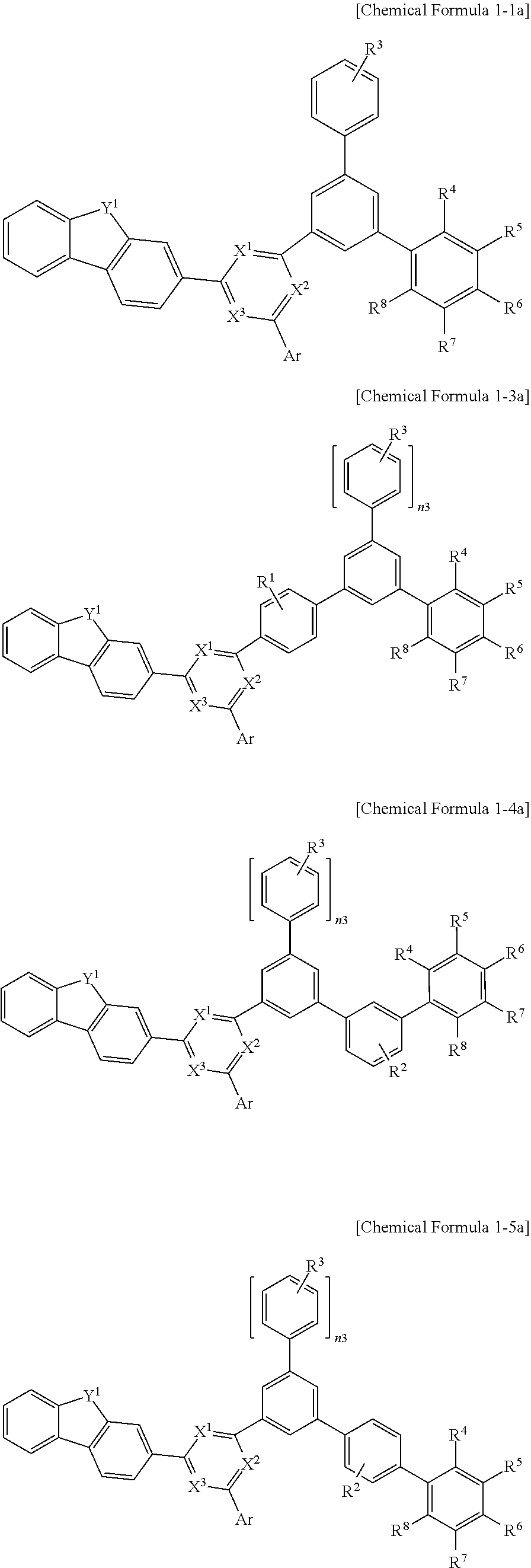
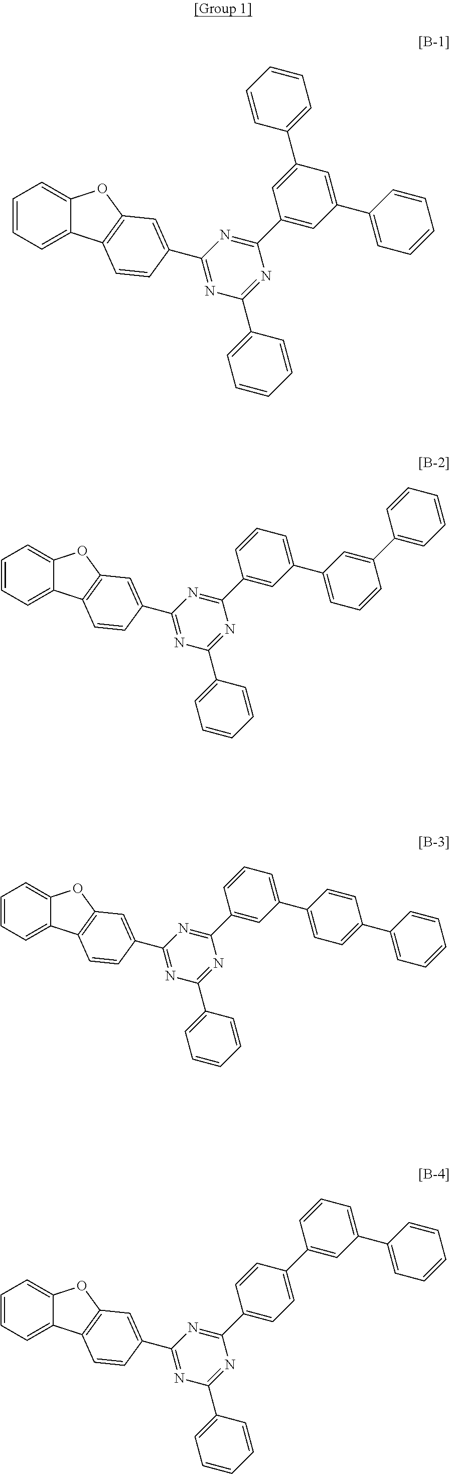


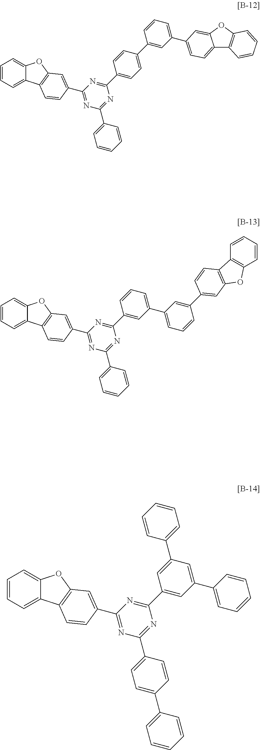


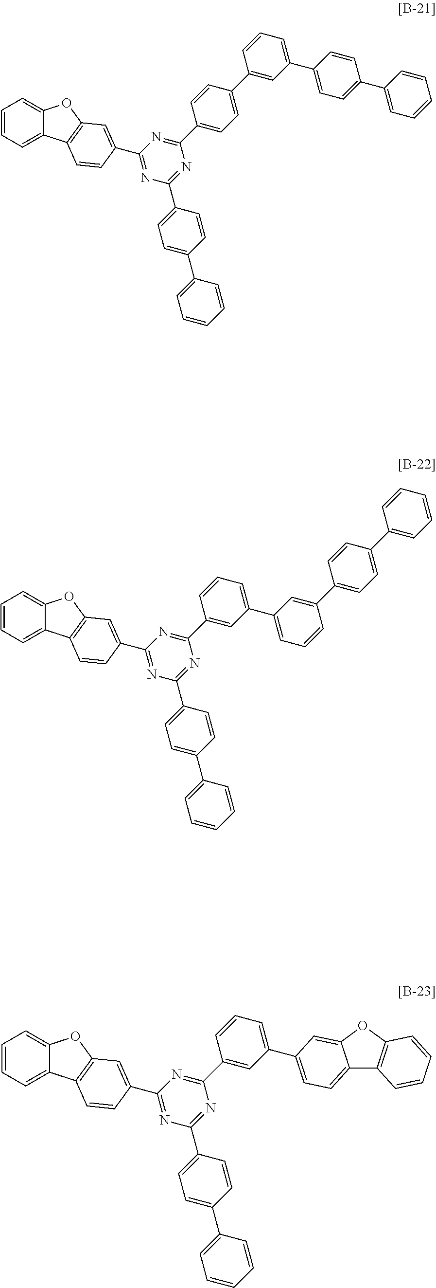


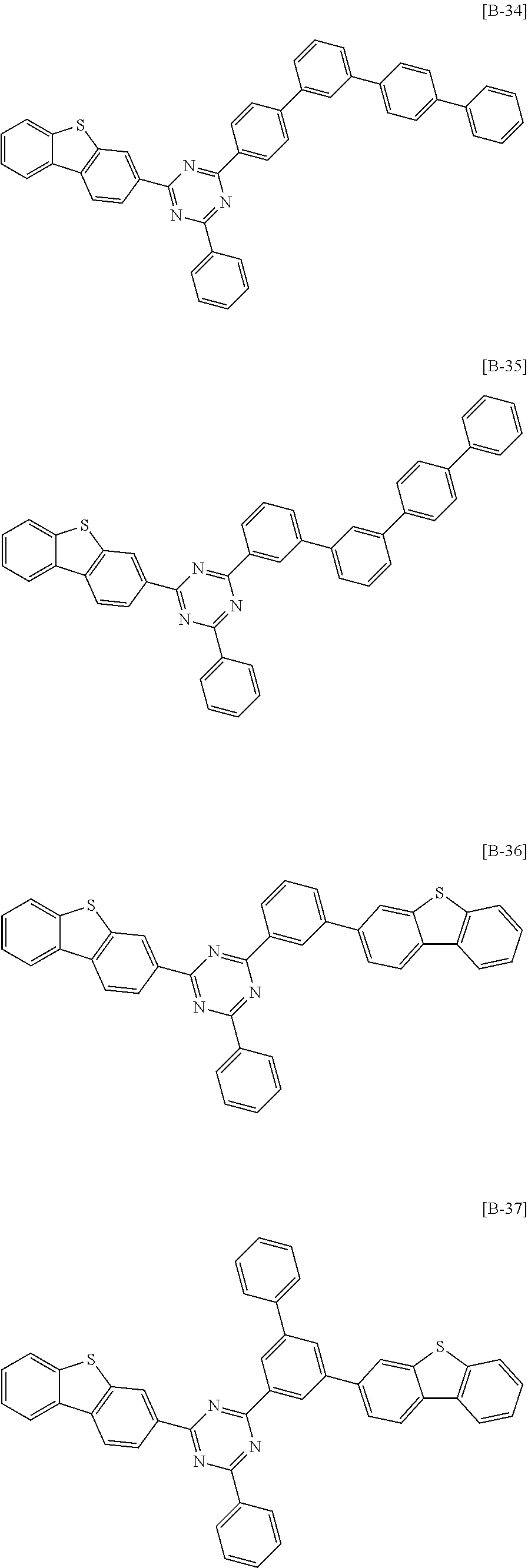
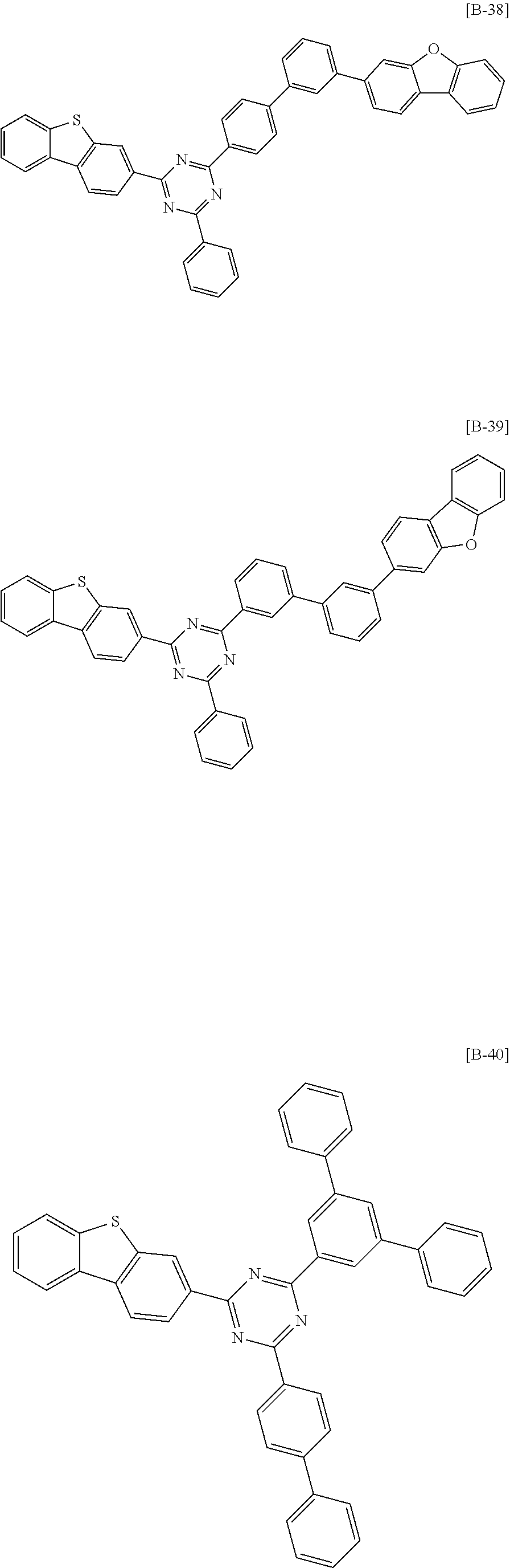
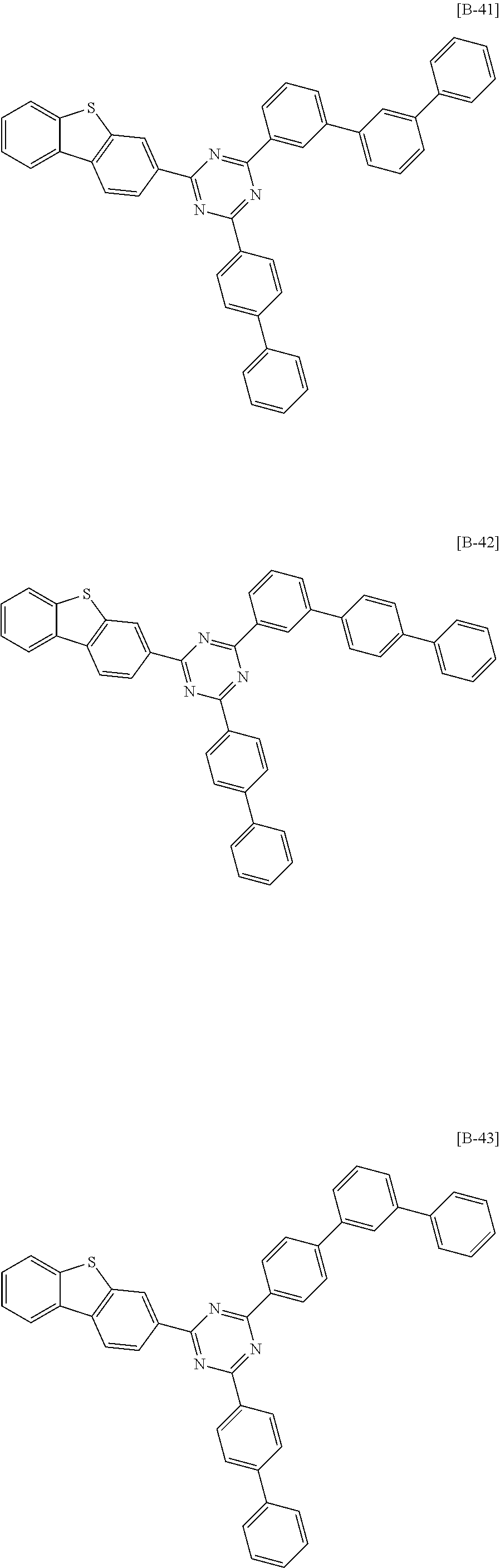


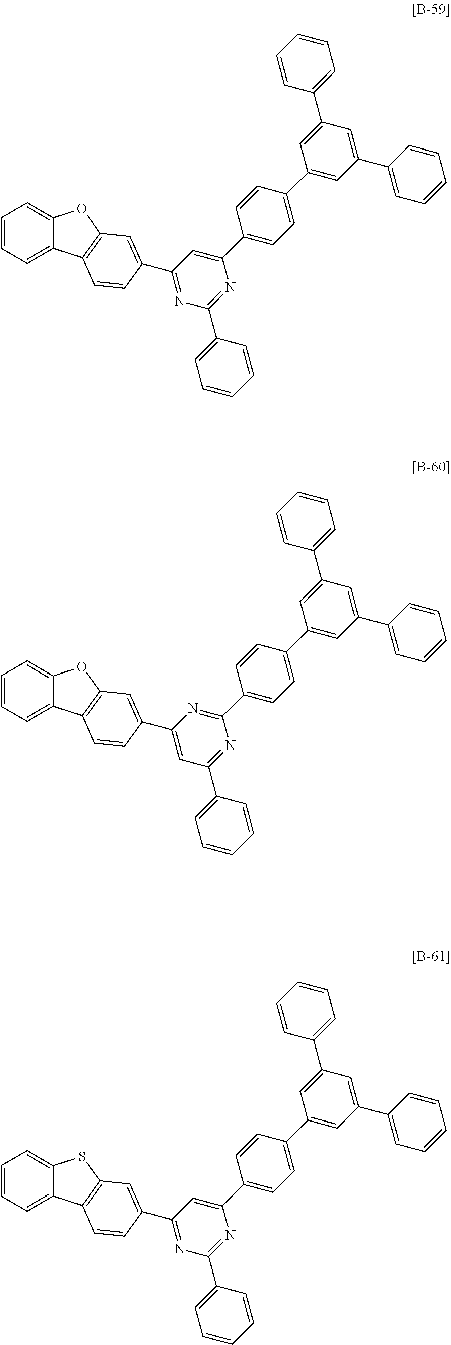
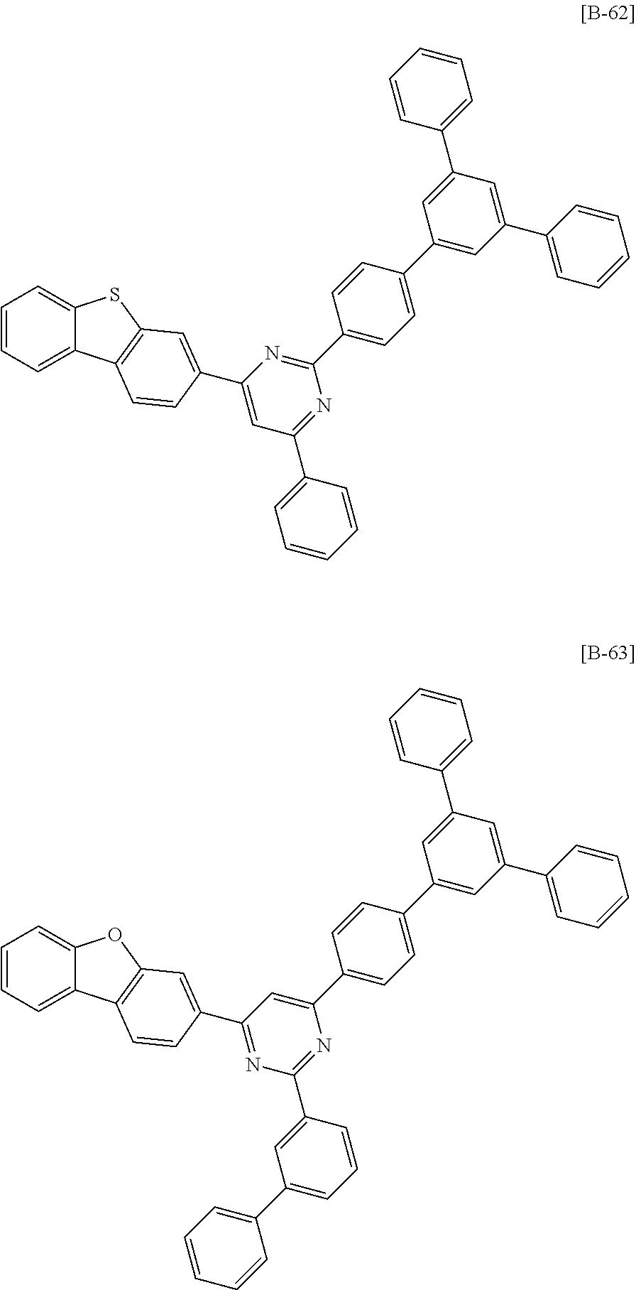


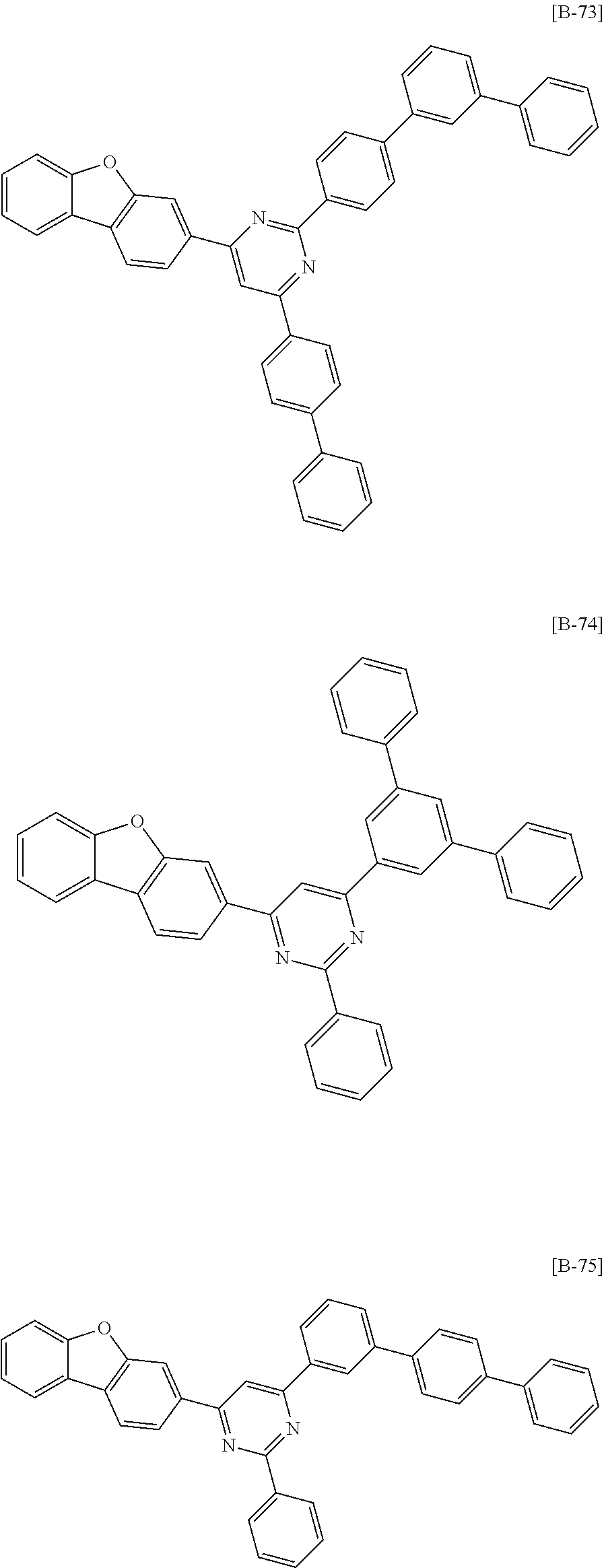


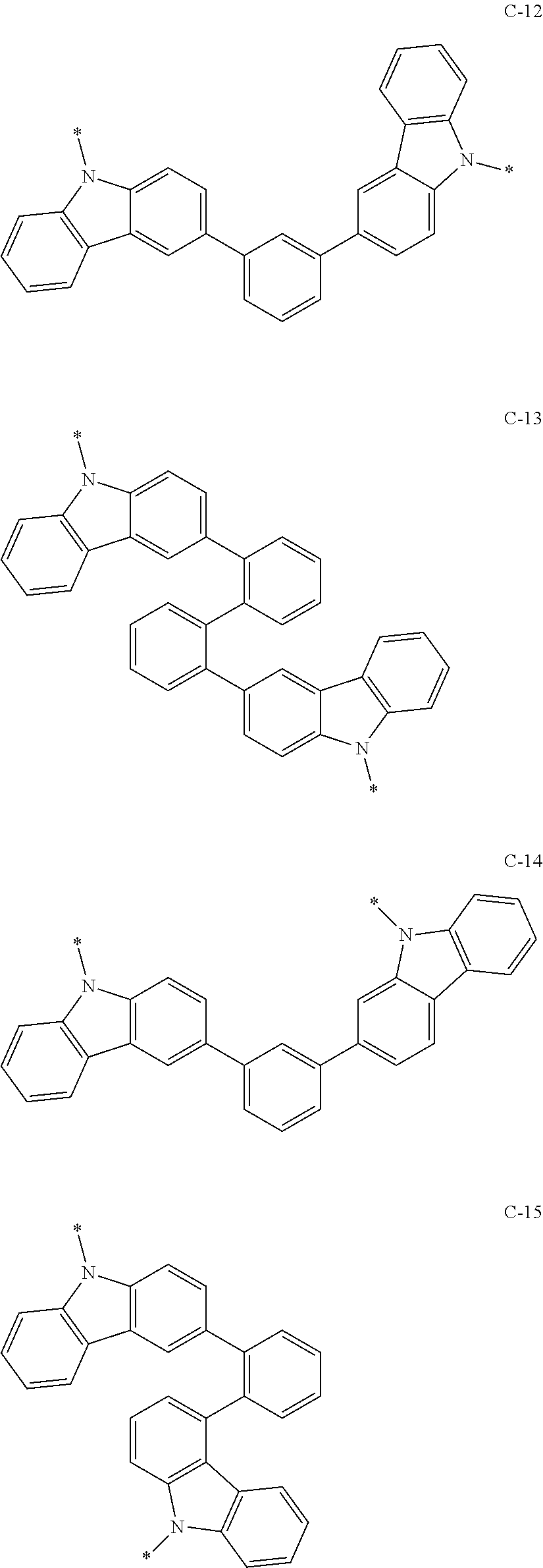
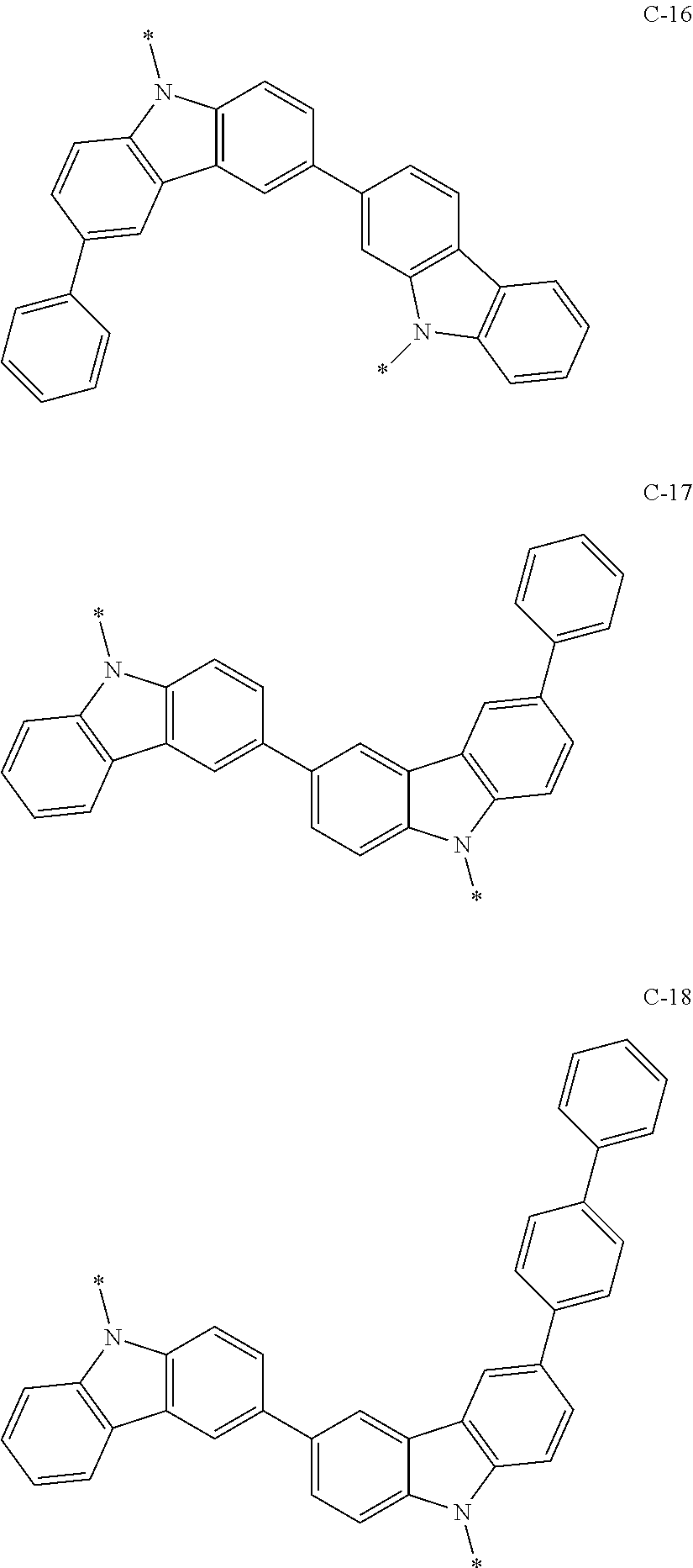

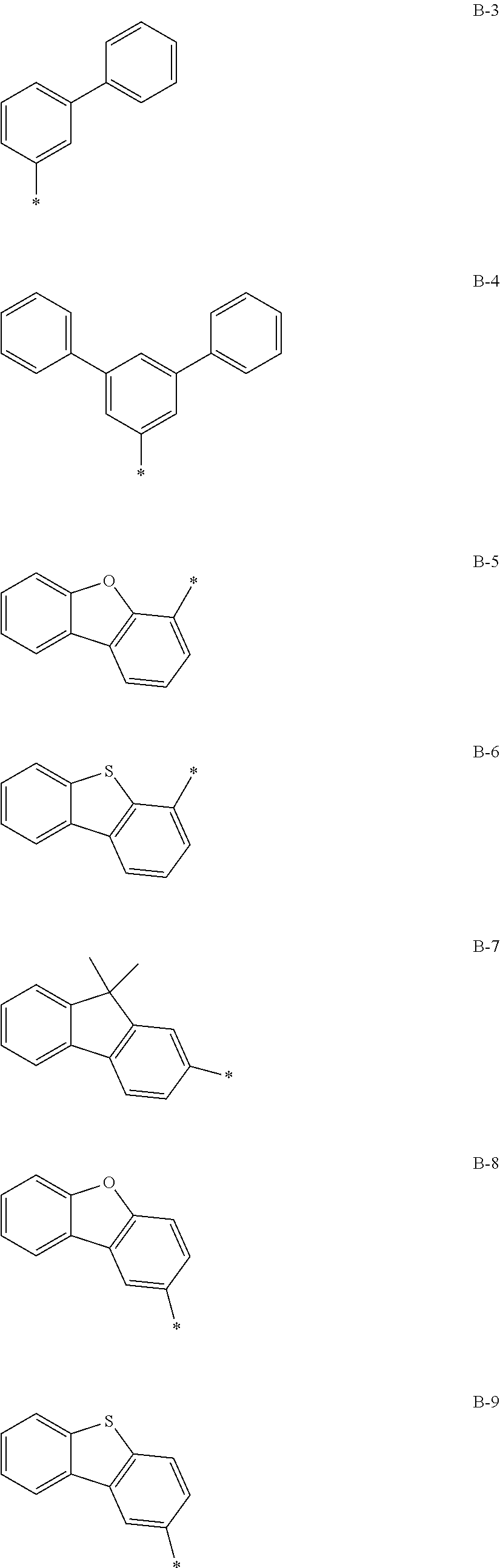


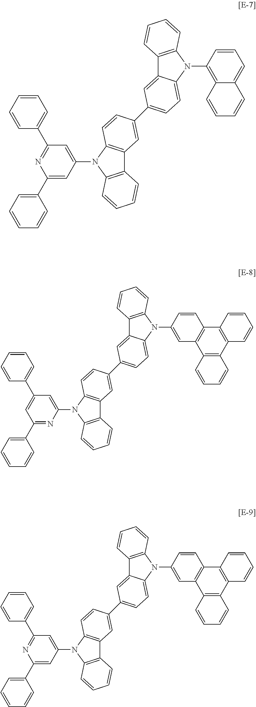
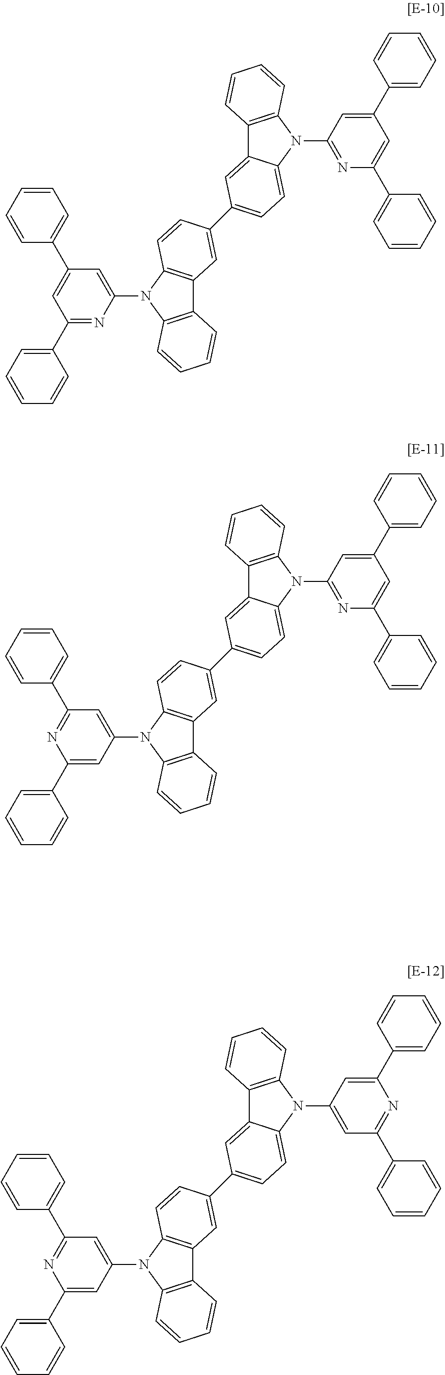
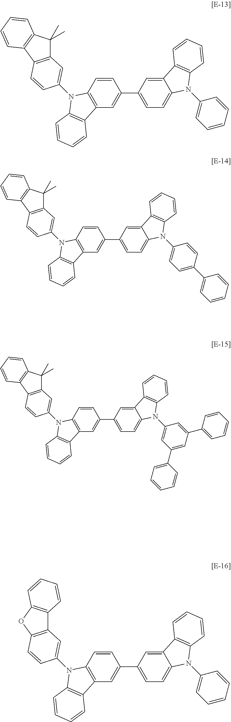


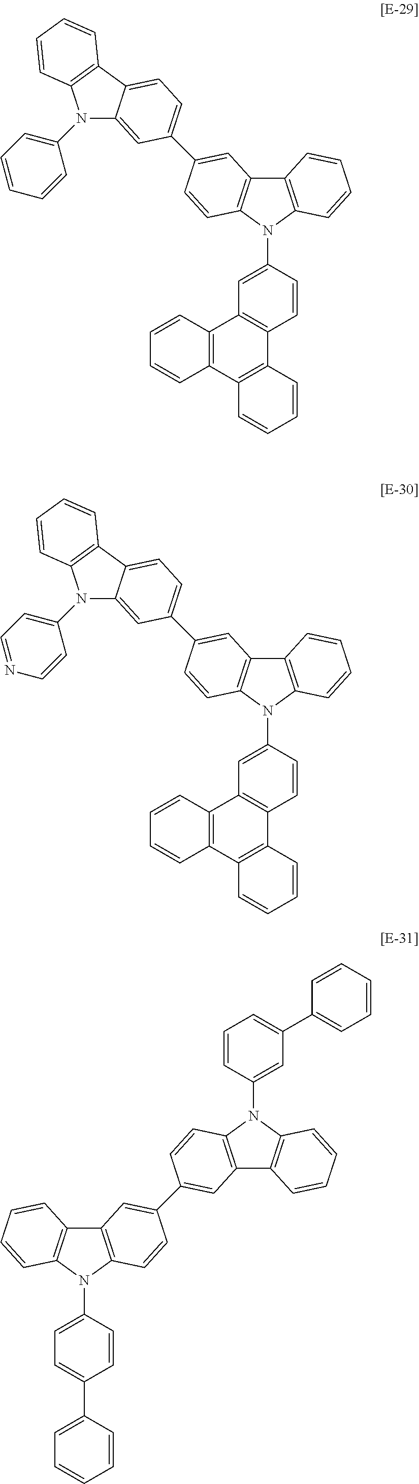
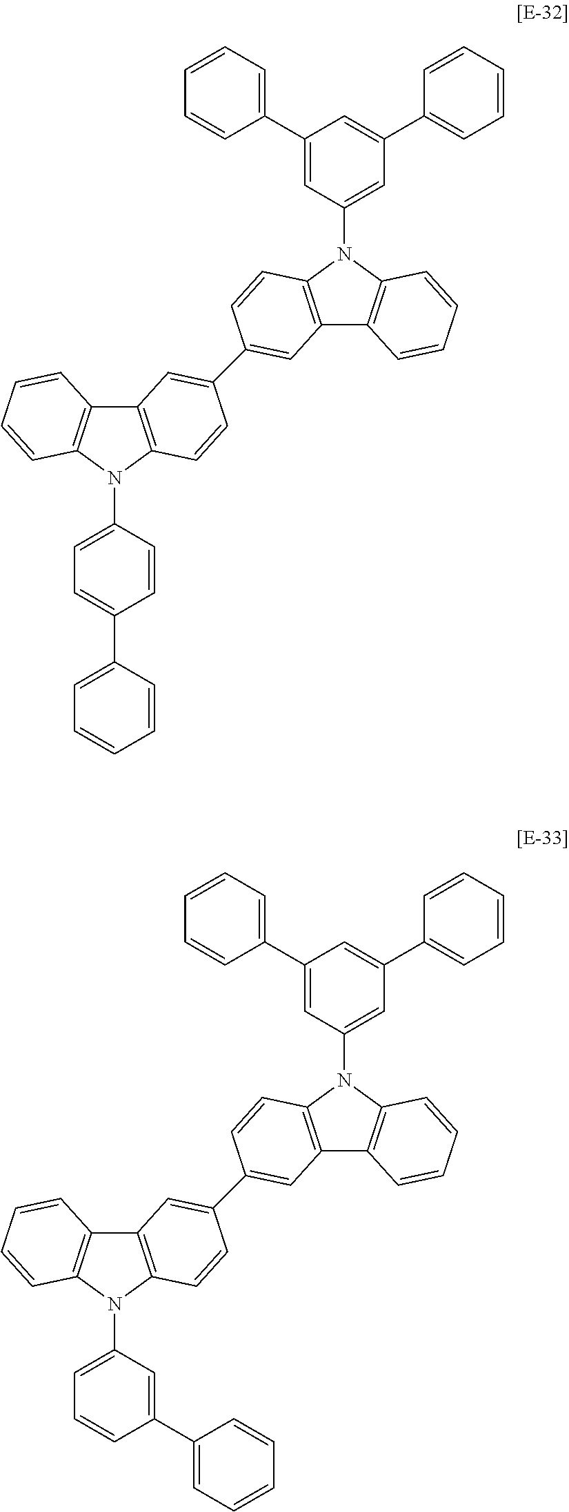

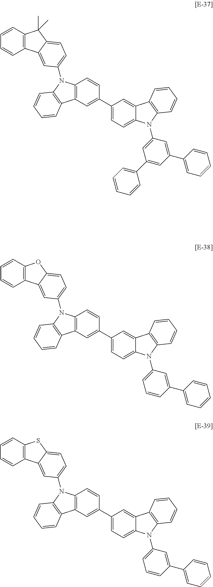

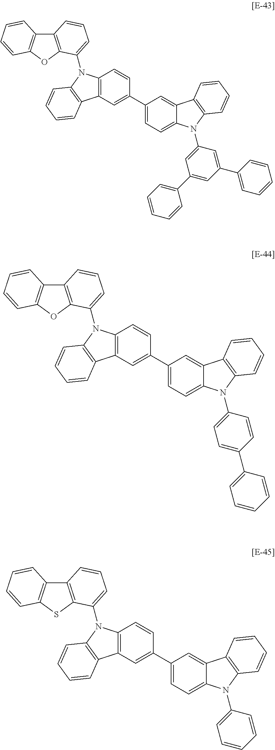

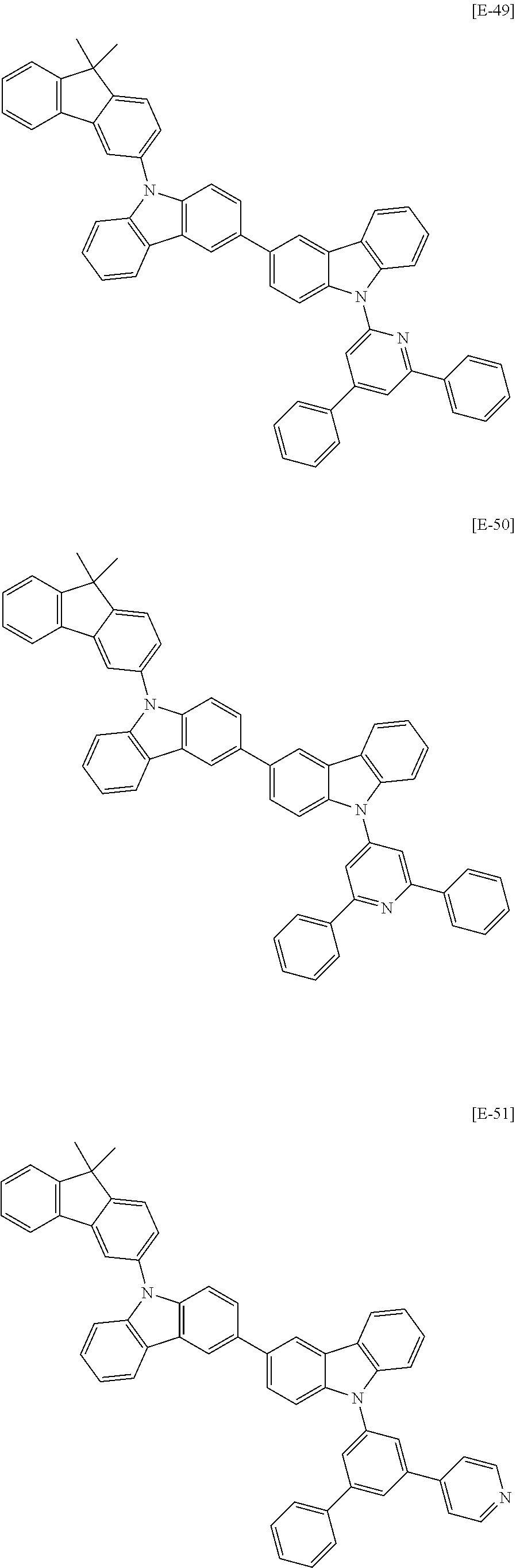


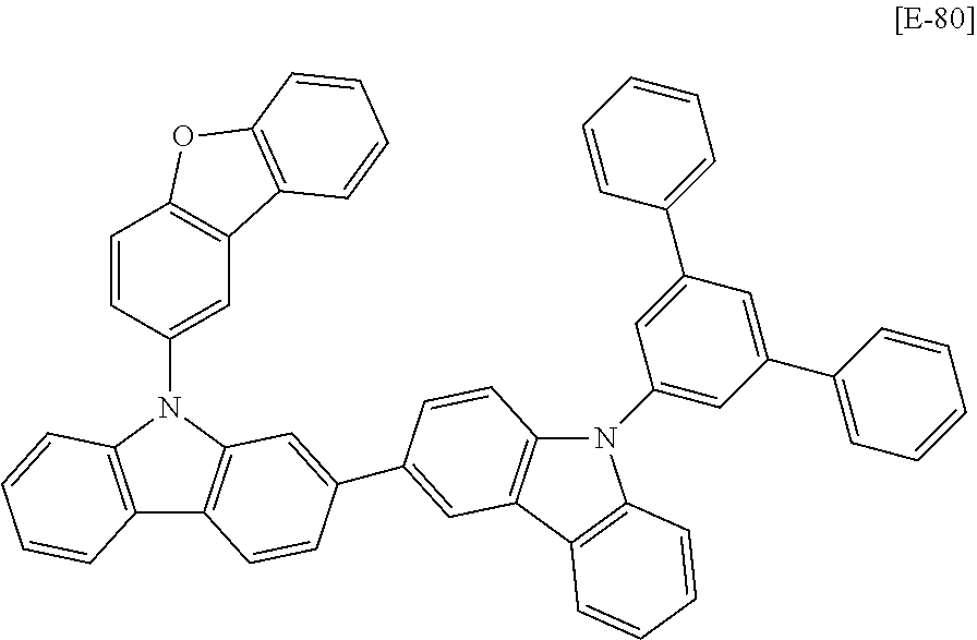


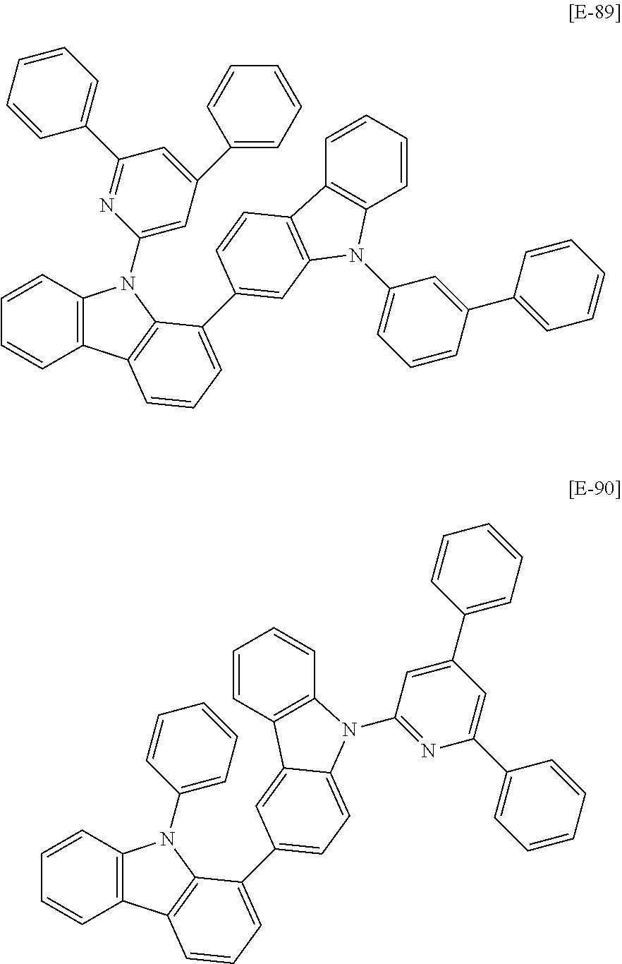

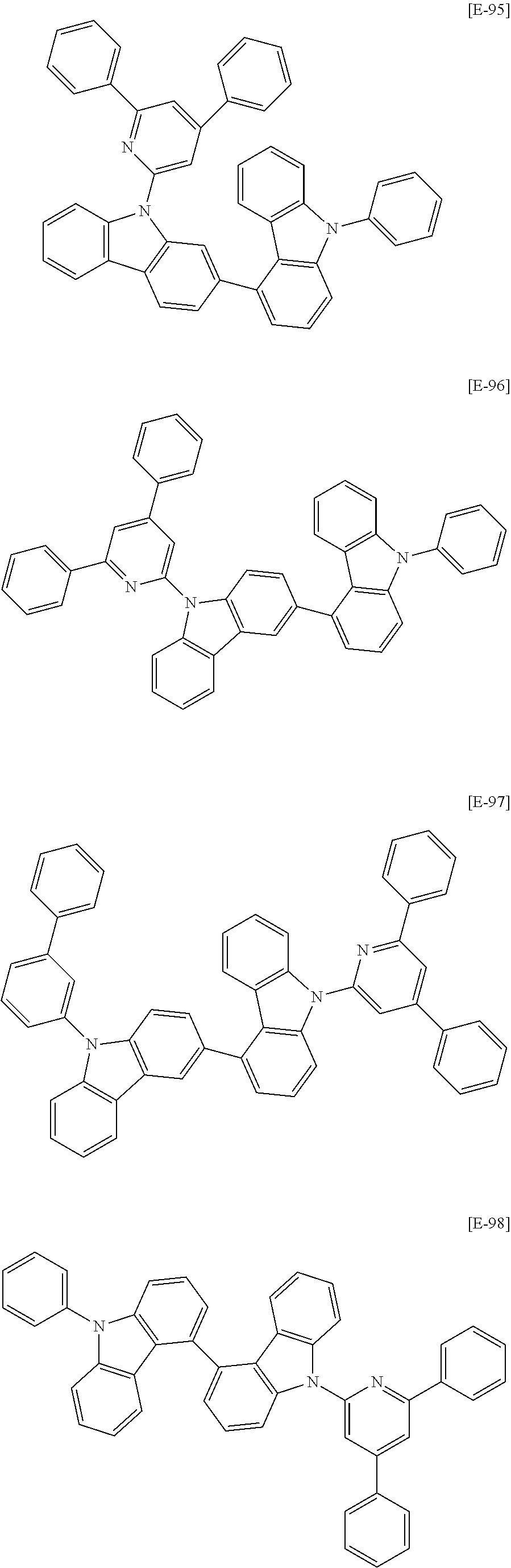
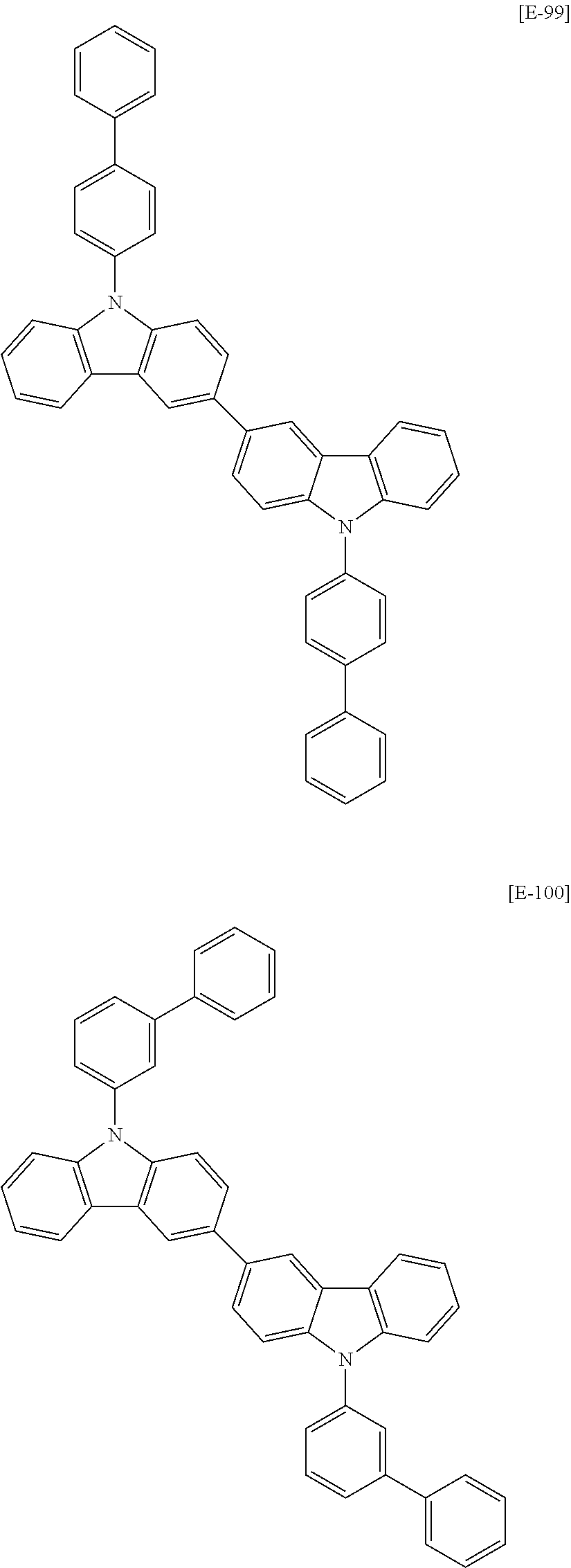


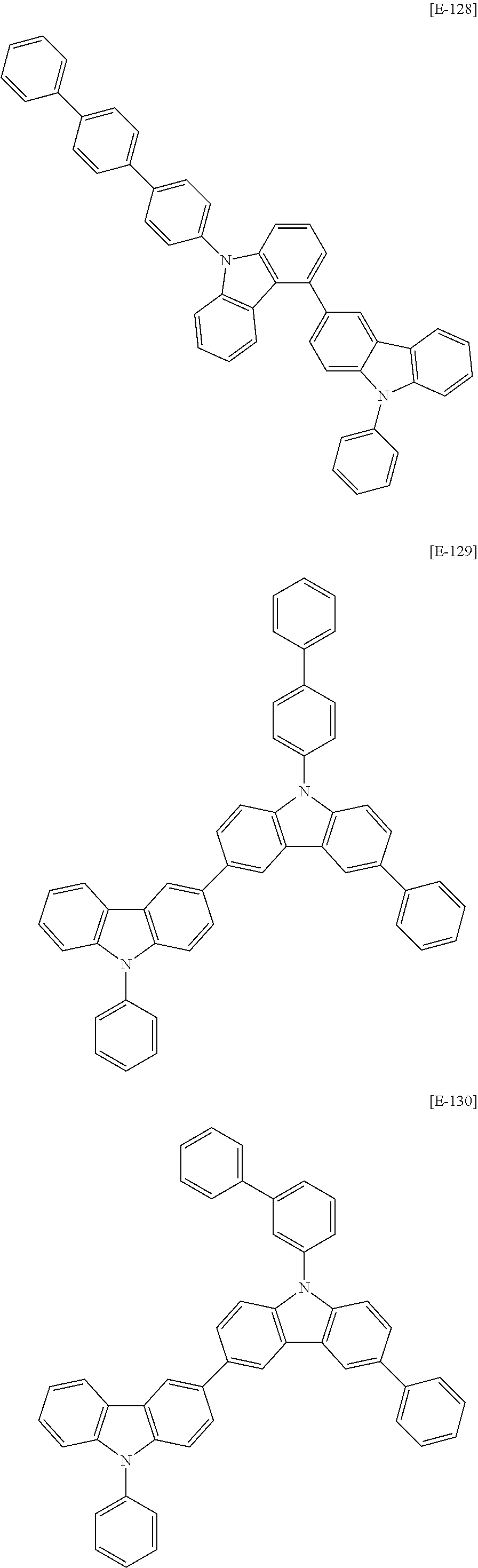


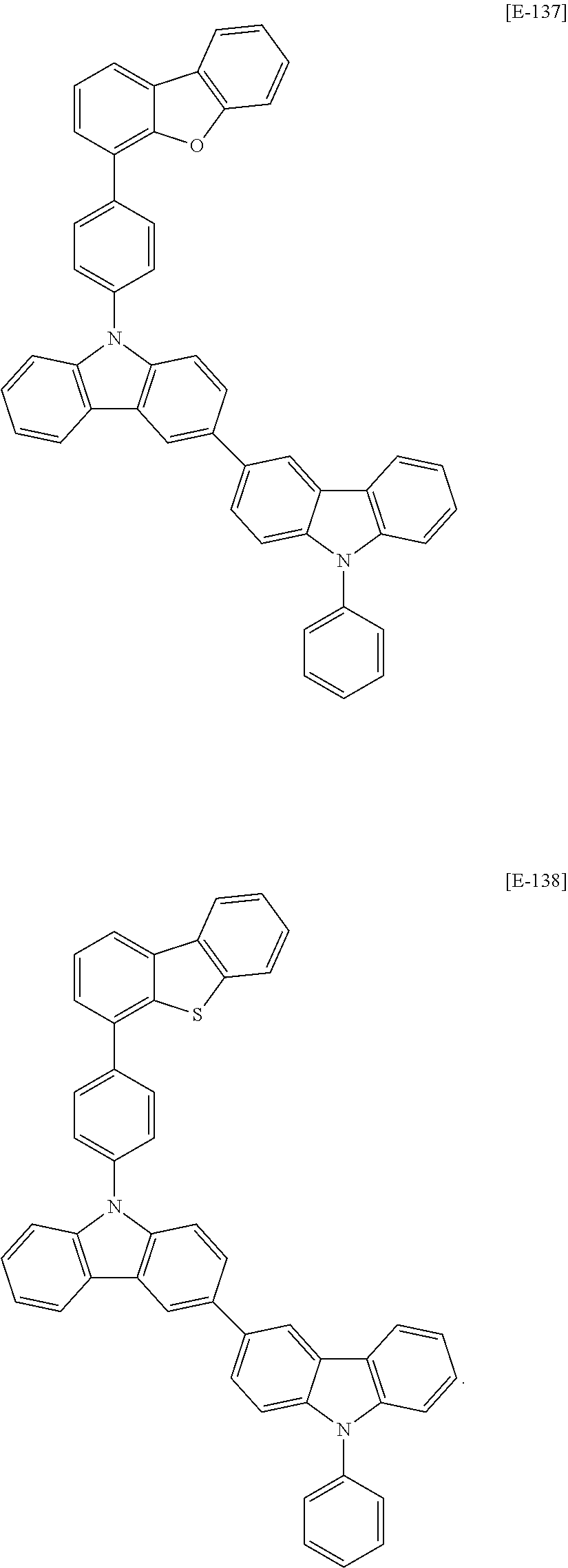
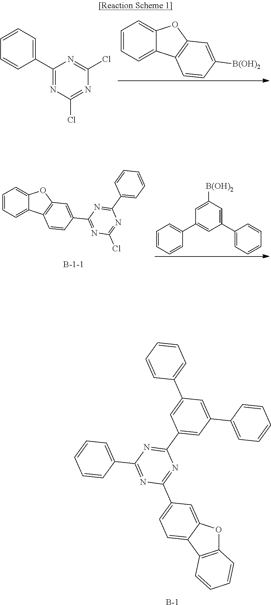


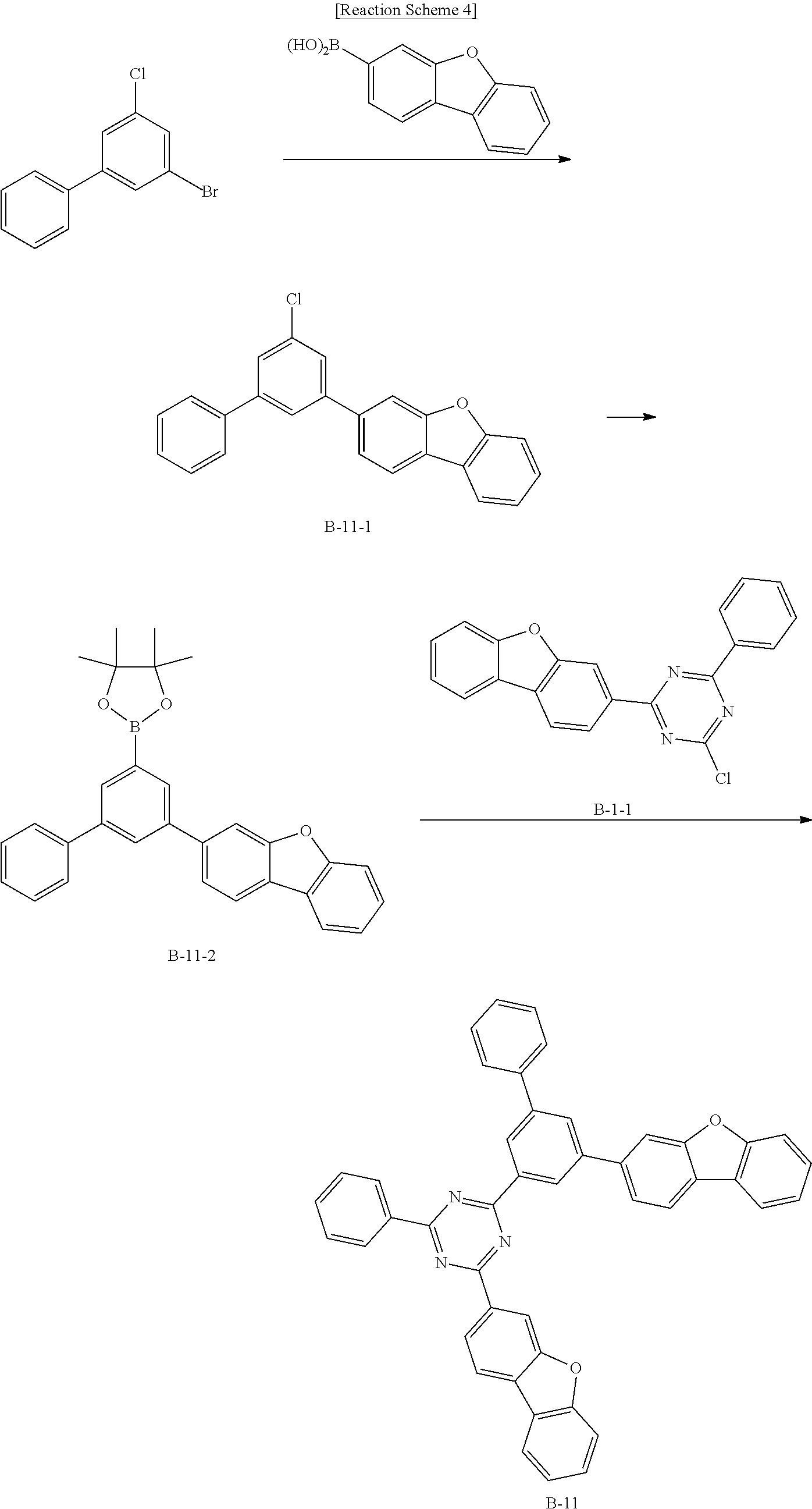
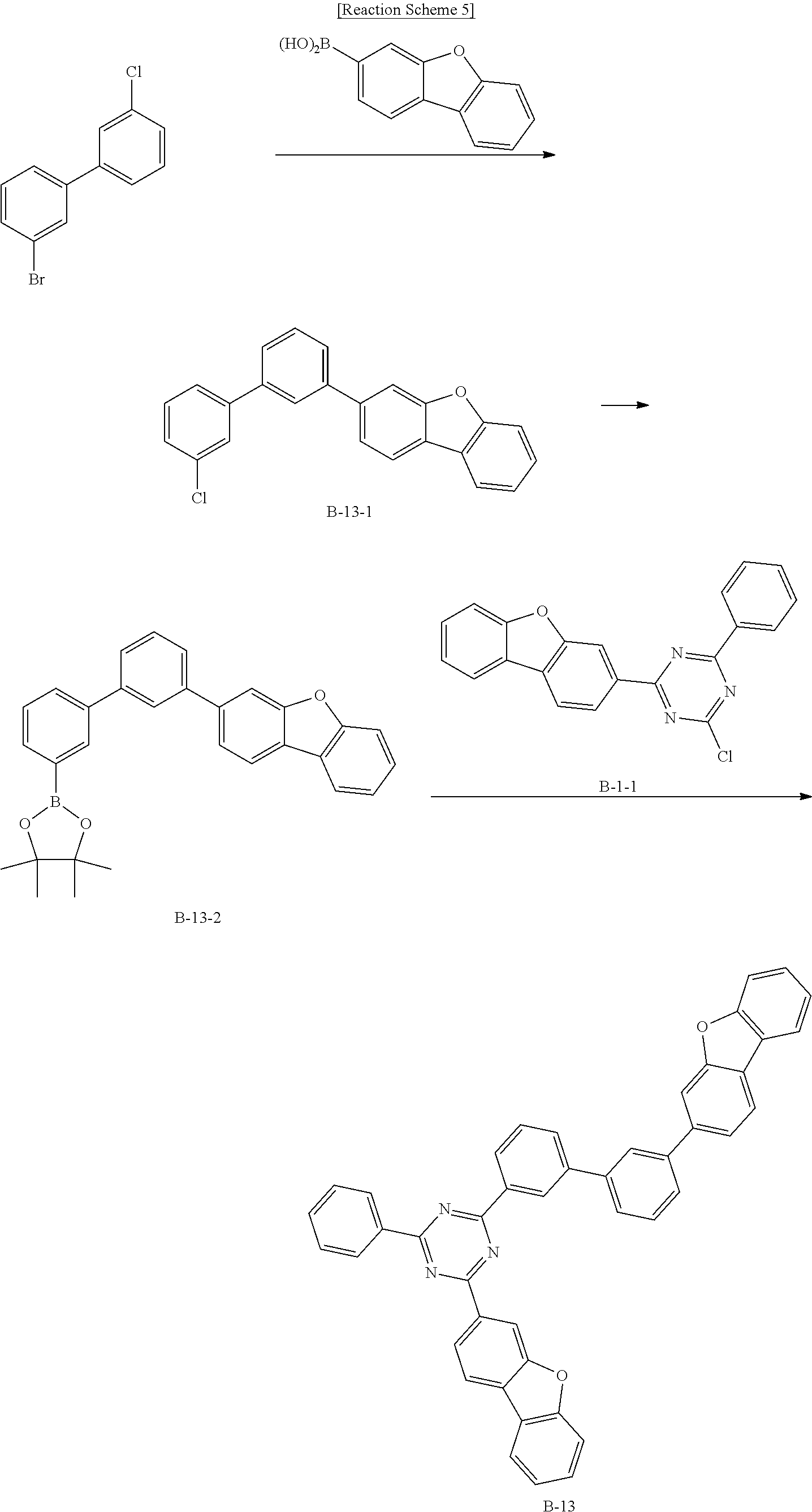

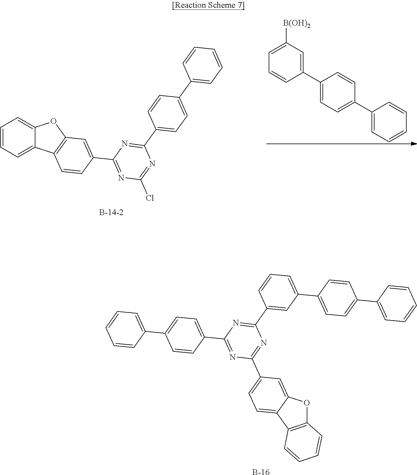

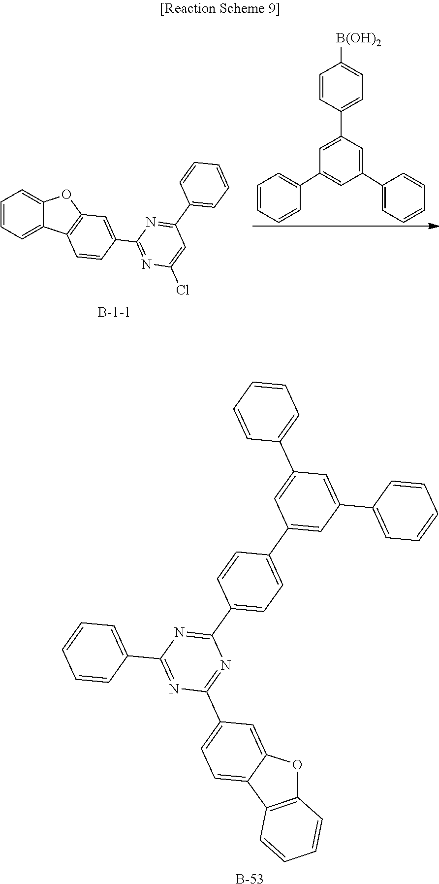


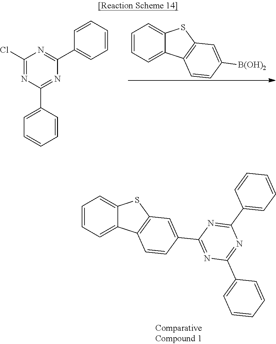
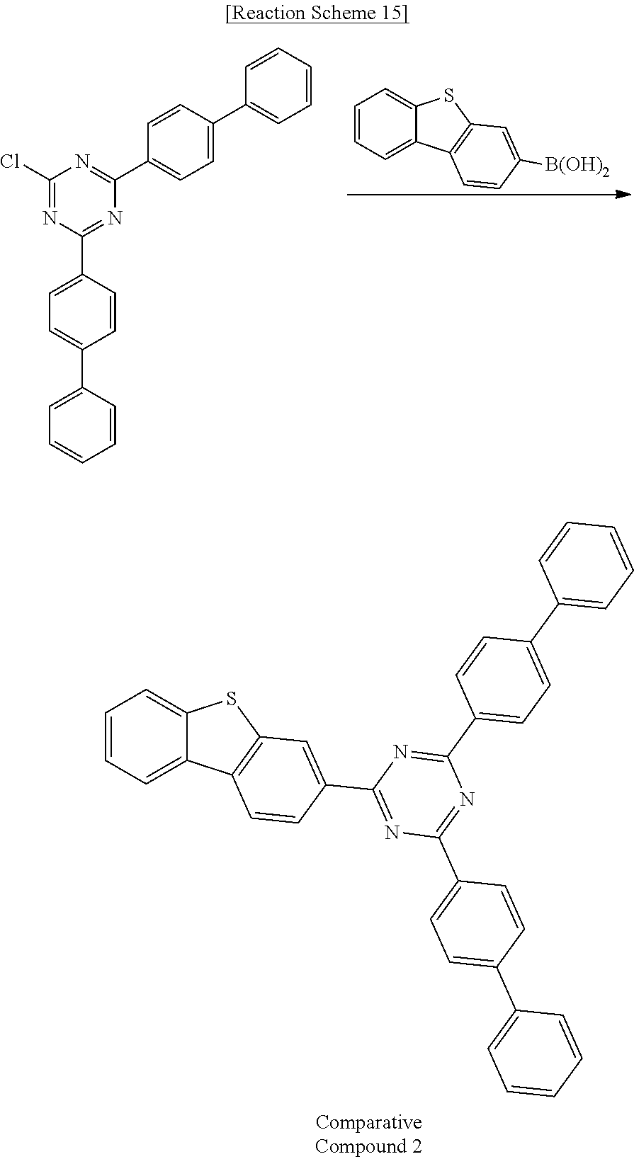

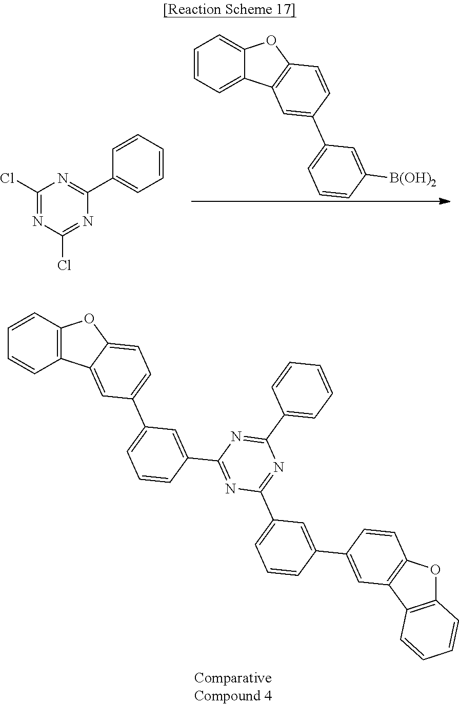


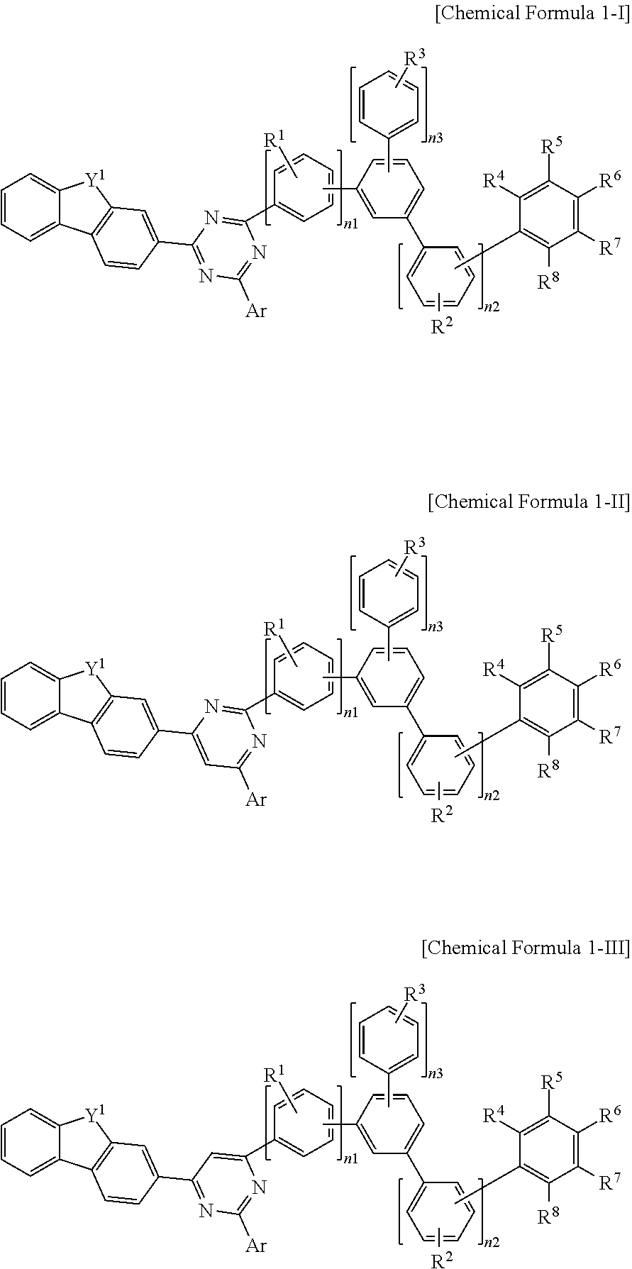


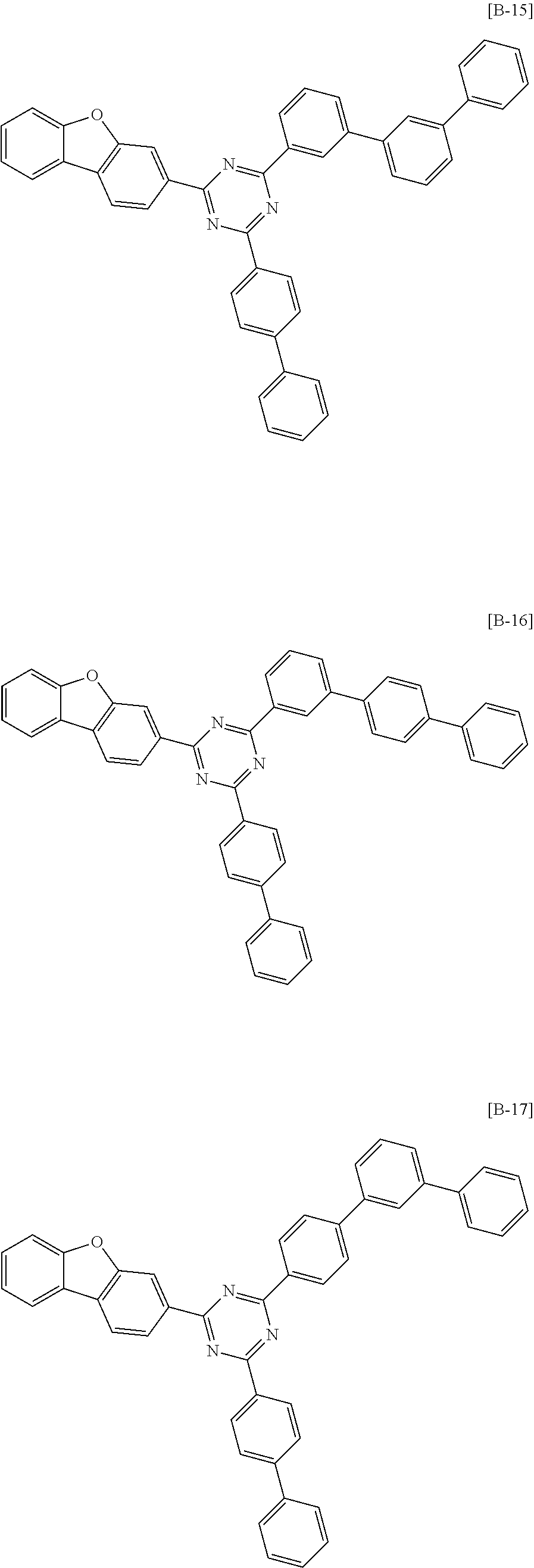
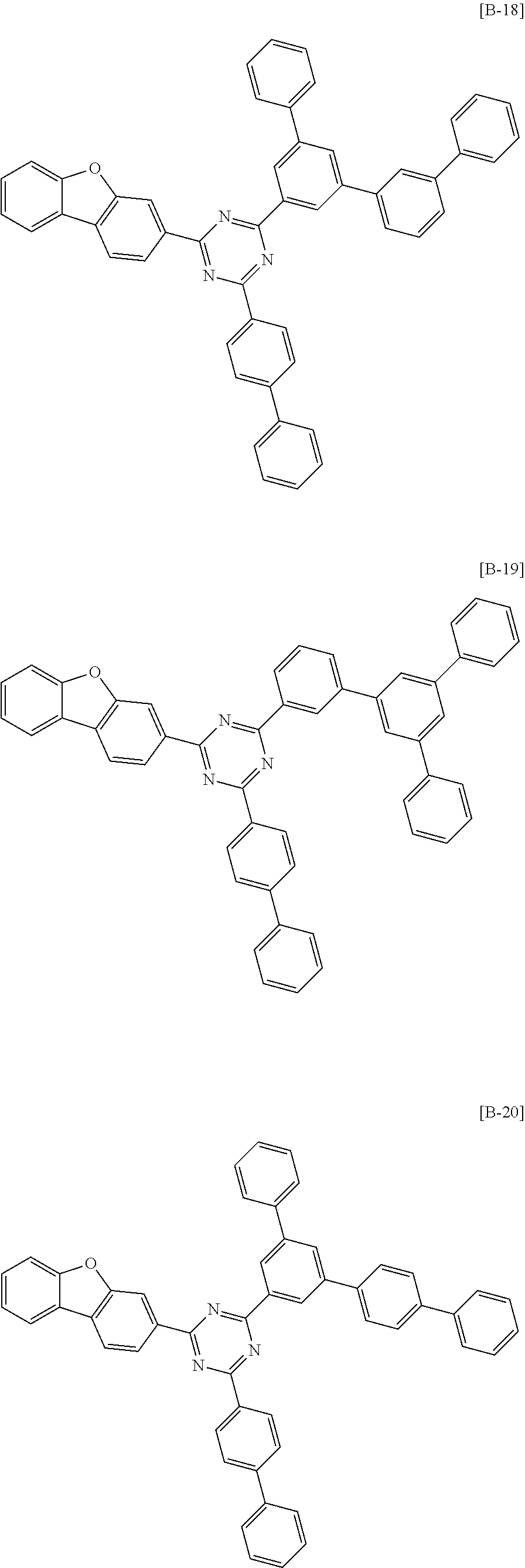

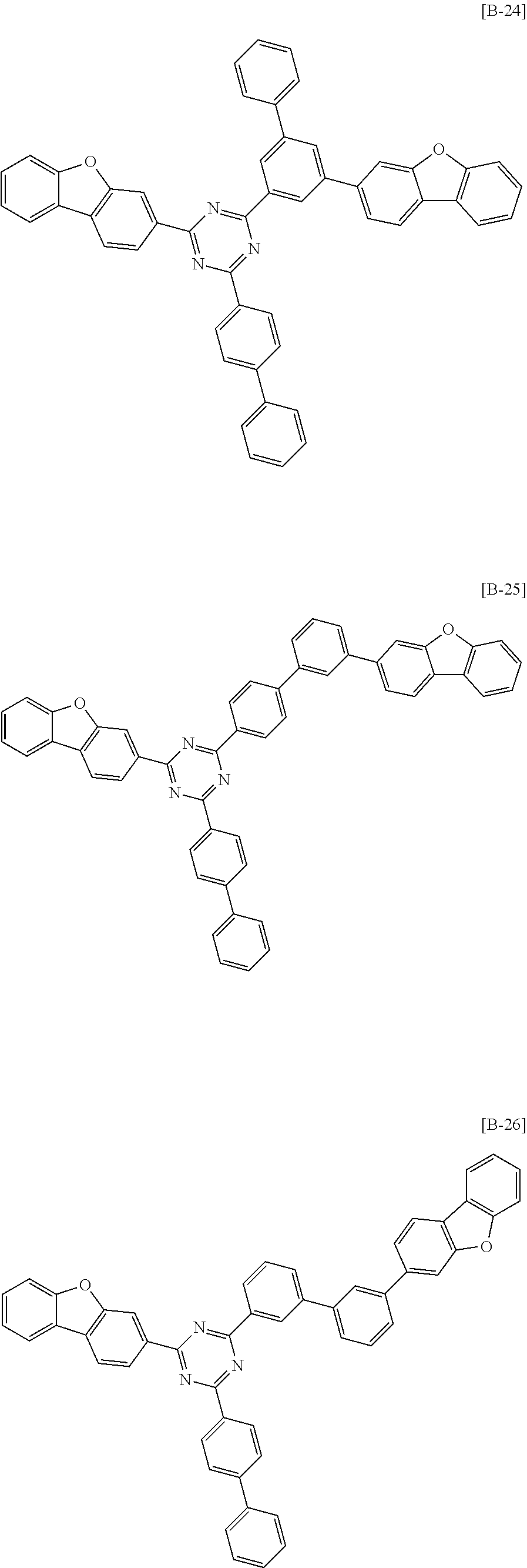
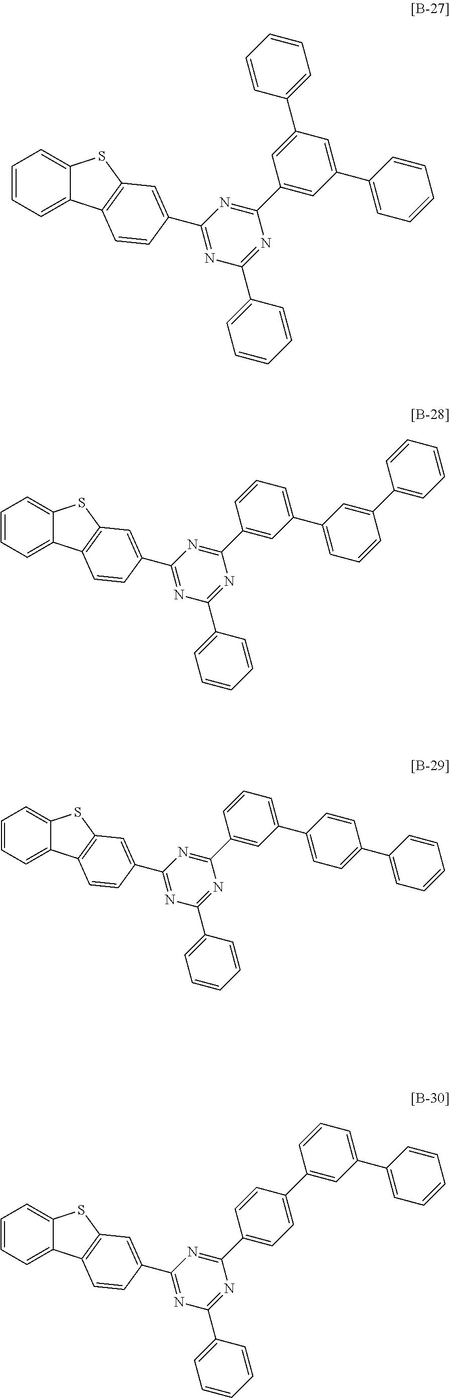


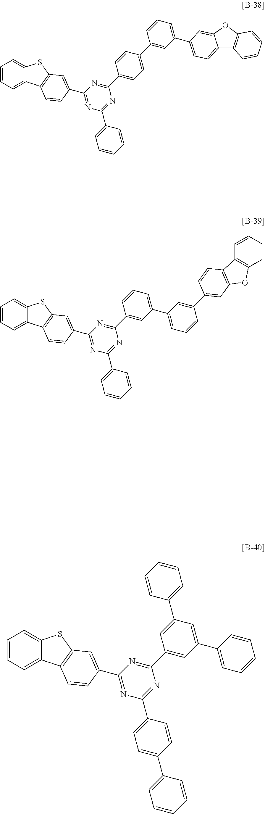


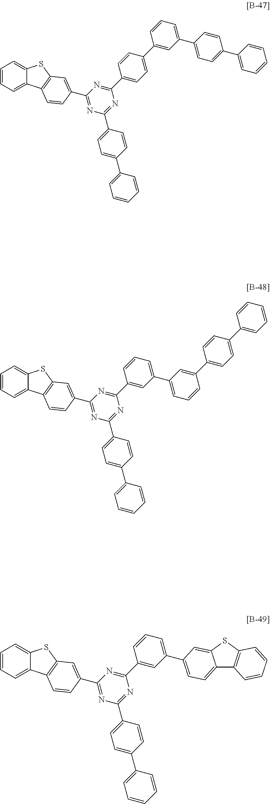
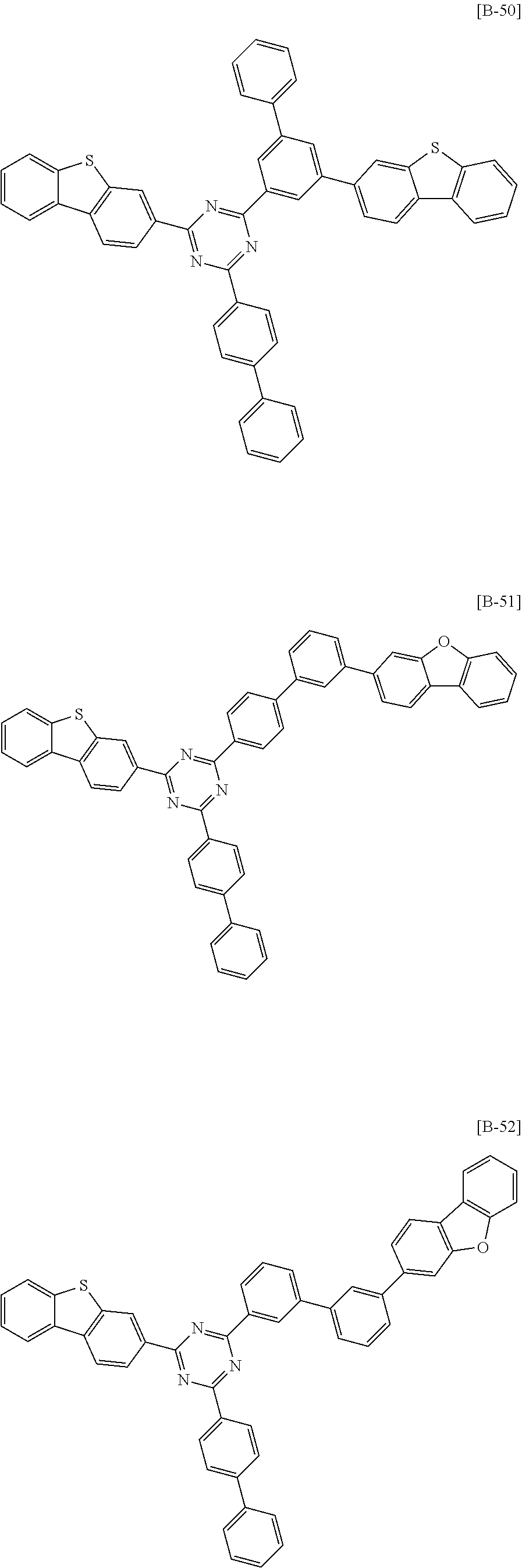

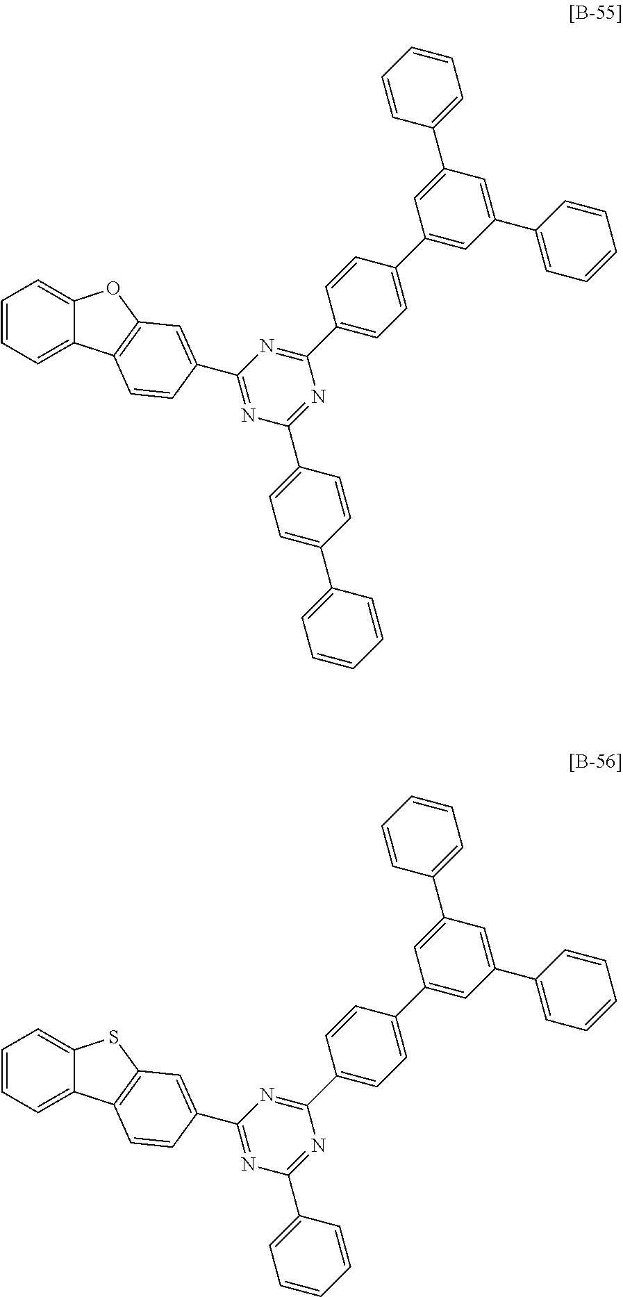
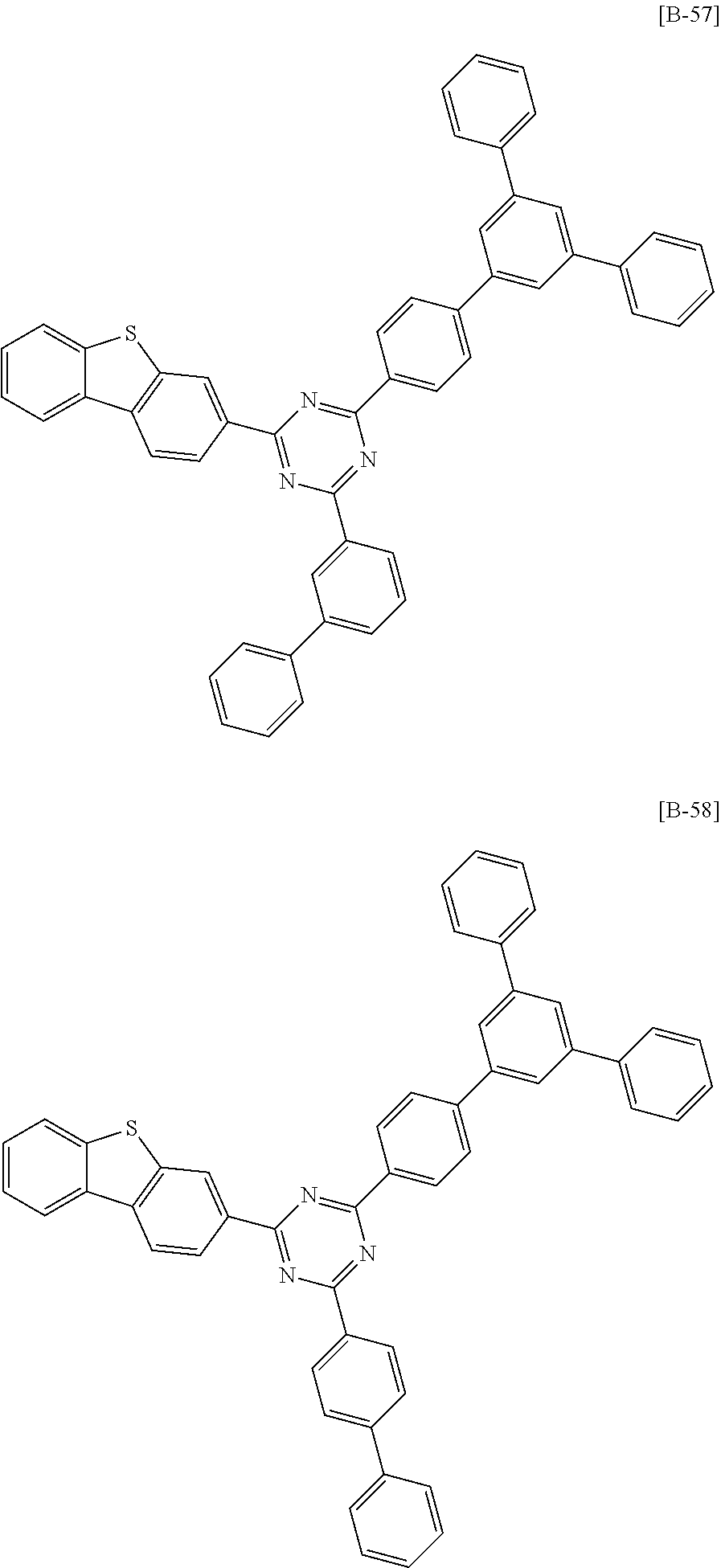
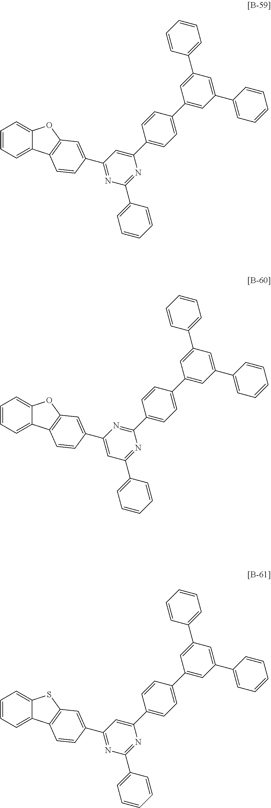


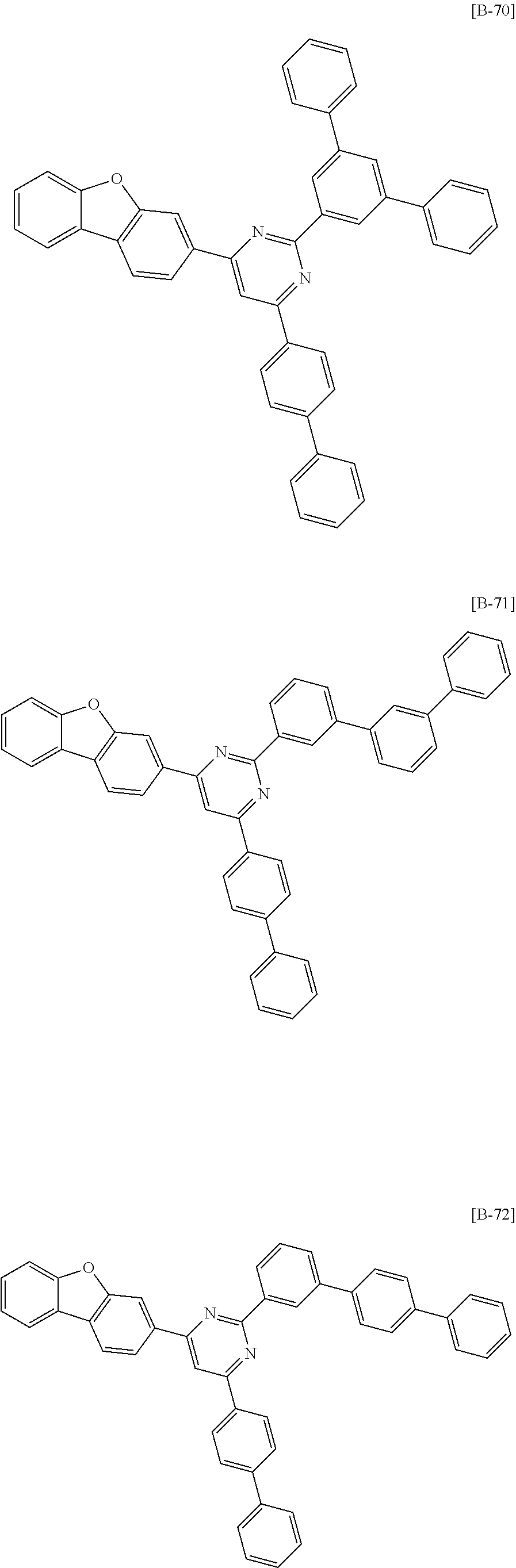

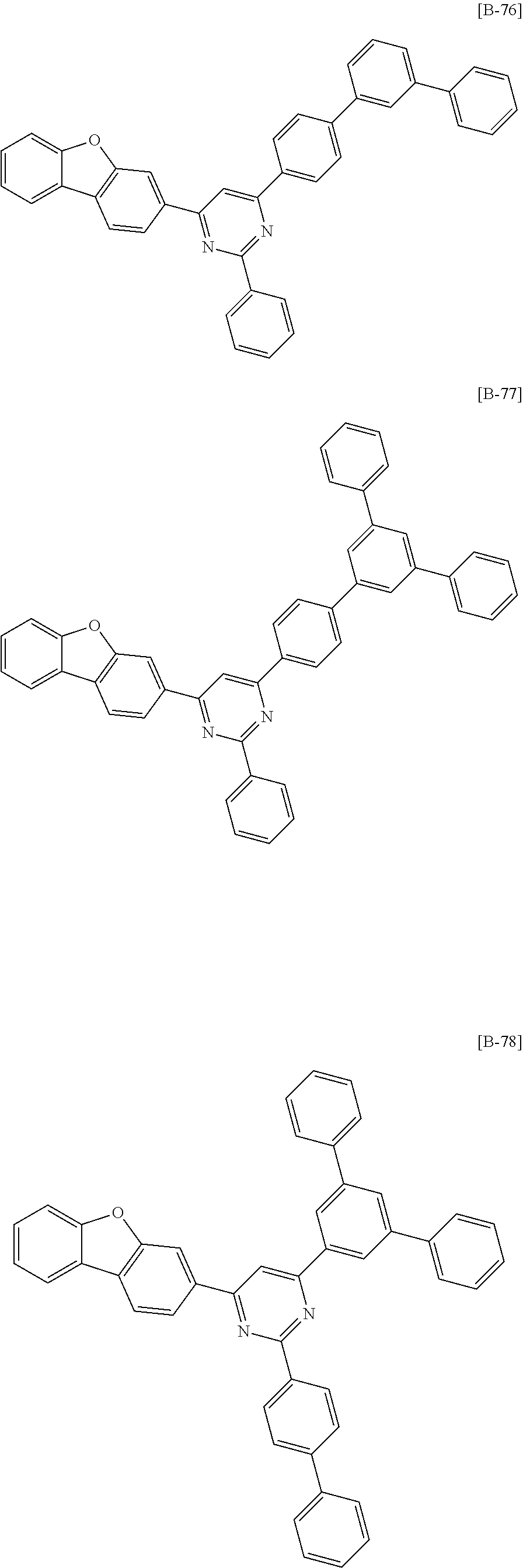
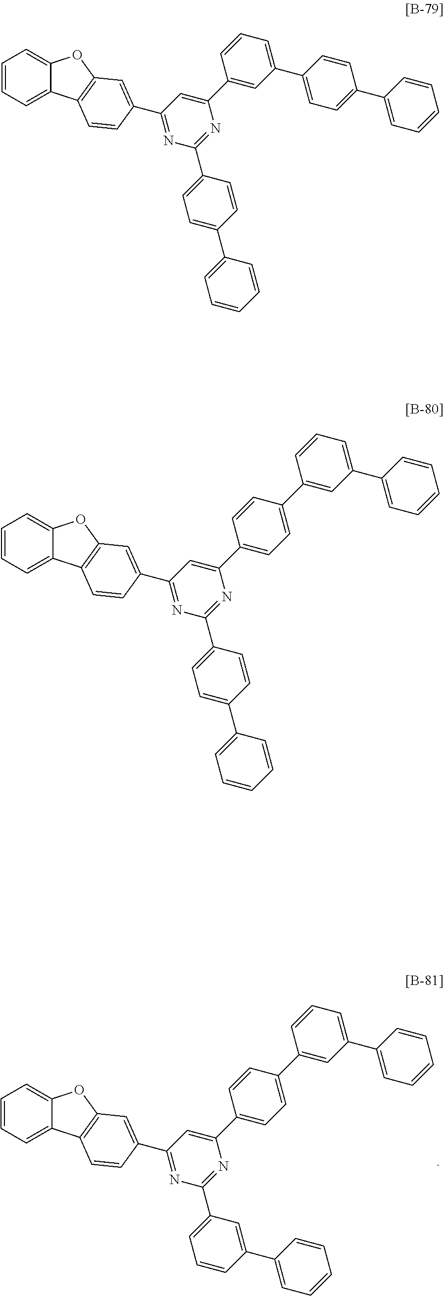

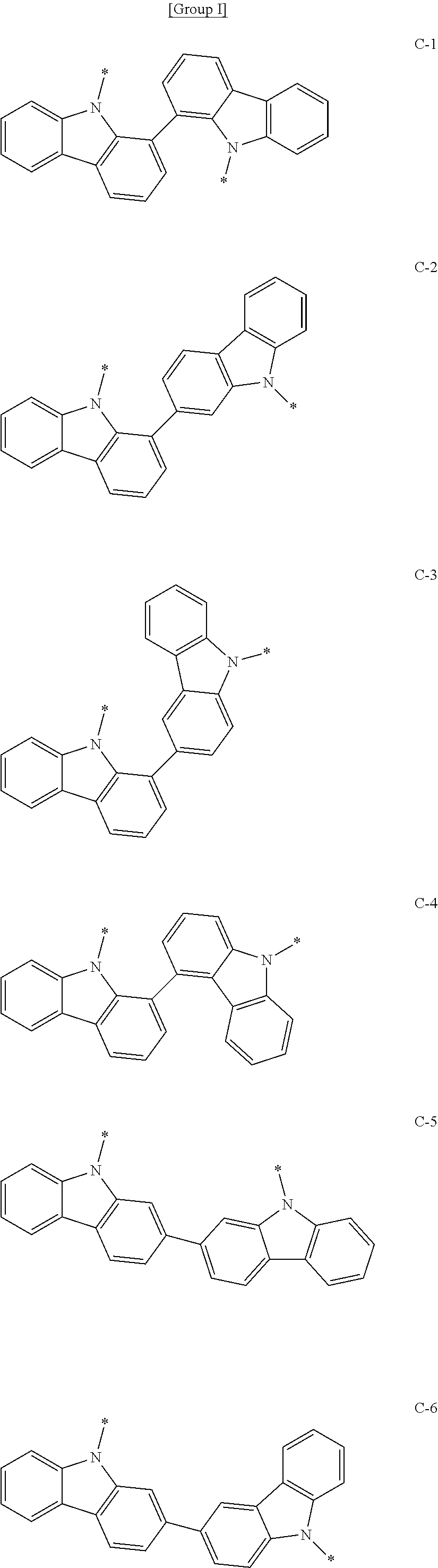
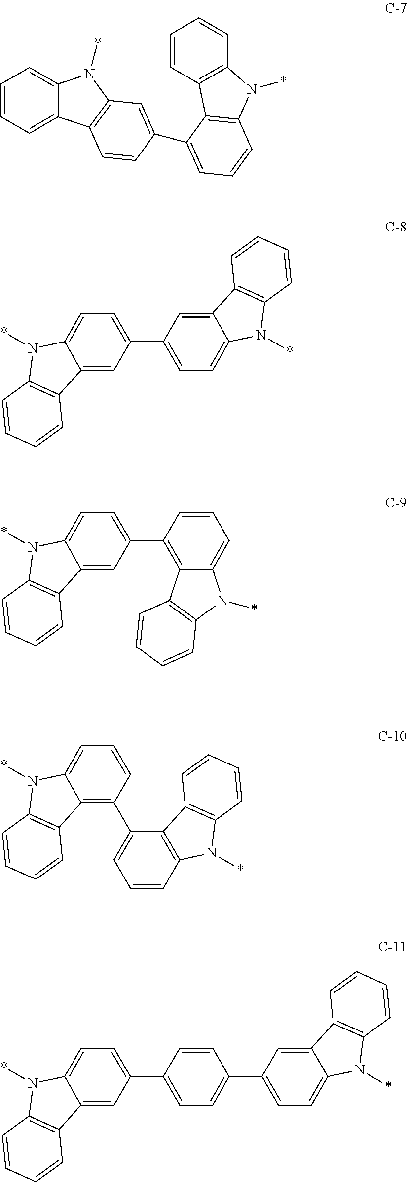
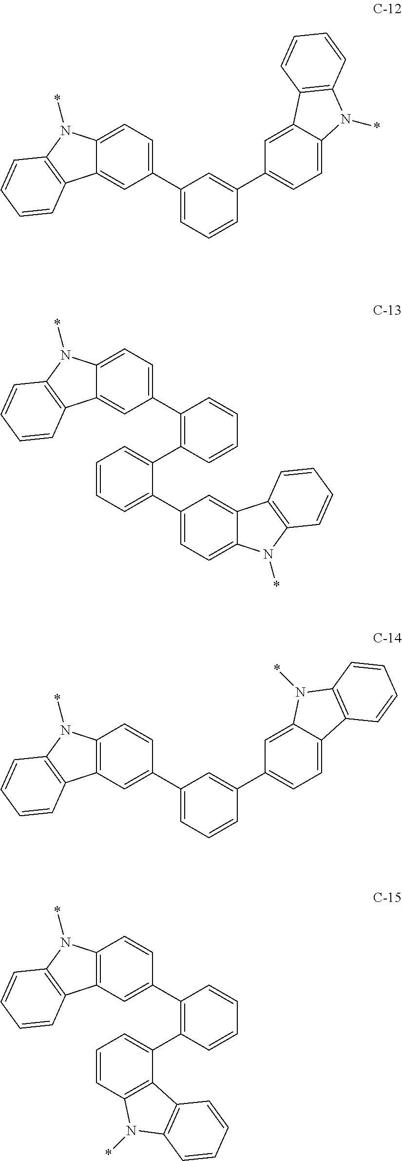


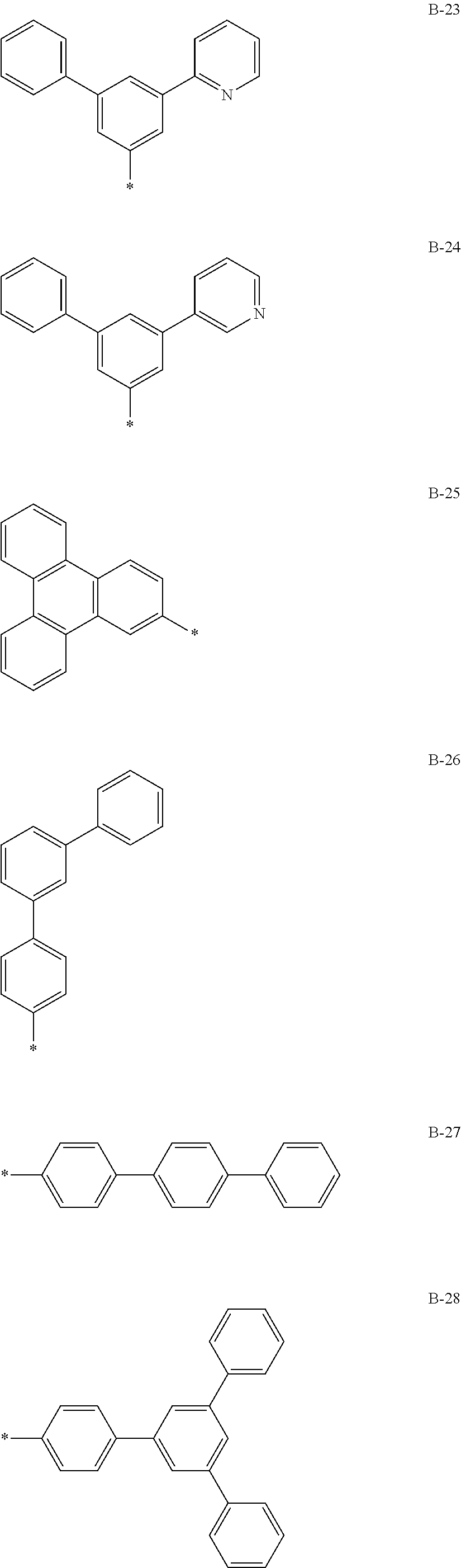
D00000
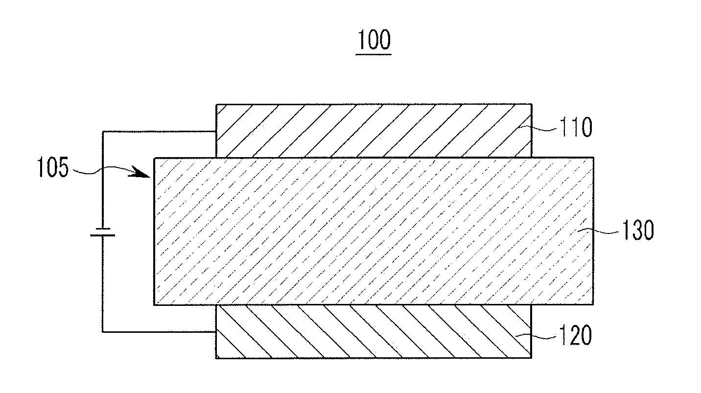
D00001

XML
uspto.report is an independent third-party trademark research tool that is not affiliated, endorsed, or sponsored by the United States Patent and Trademark Office (USPTO) or any other governmental organization. The information provided by uspto.report is based on publicly available data at the time of writing and is intended for informational purposes only.
While we strive to provide accurate and up-to-date information, we do not guarantee the accuracy, completeness, reliability, or suitability of the information displayed on this site. The use of this site is at your own risk. Any reliance you place on such information is therefore strictly at your own risk.
All official trademark data, including owner information, should be verified by visiting the official USPTO website at www.uspto.gov. This site is not intended to replace professional legal advice and should not be used as a substitute for consulting with a legal professional who is knowledgeable about trademark law.