Light Emitting Device And Method Of Forming The Same
HSIEH; Min-Hsun ; et al.
U.S. patent application number 16/254342 was filed with the patent office on 2019-05-23 for light emitting device and method of forming the same. The applicant listed for this patent is EPISTAR CORPORATION. Invention is credited to Min-Hsun HSIEH, Chih-Chiang LU, Ching-Pu TAI.
| Application Number | 20190157498 16/254342 |
| Document ID | / |
| Family ID | 38321383 |
| Filed Date | 2019-05-23 |


| United States Patent Application | 20190157498 |
| Kind Code | A1 |
| HSIEH; Min-Hsun ; et al. | May 23, 2019 |
LIGHT EMITTING DEVICE AND METHOD OF FORMING THE SAME
Abstract
A light-emitting device includes a transparent substrate, a transparent adhesive layer on the transparent substrate, a first transparent conductive layer on the transparent adhesive layer, a multi-layer epitaxial structure and a first electrode on the transparent conductive layer, and a second electrode on the multi-layer epitaxial structure. The multi-layer epitaxial structure includes a light-emitting layer. The transparent substrate has a first surface facing the transparent adhesive layer and a second surface opposite to the first surface, wherein the area of the second surface is larger than that of the light-emitting layer, and the area ratio thereof is not less than 1.6.
| Inventors: | HSIEH; Min-Hsun; (Hsinchu, TW) ; LU; Chih-Chiang; (Hsinchu, TW) ; TAI; Ching-Pu; (Hsinchu, TW) | ||||||||||
| Applicant: |
|
||||||||||
|---|---|---|---|---|---|---|---|---|---|---|---|
| Family ID: | 38321383 | ||||||||||
| Appl. No.: | 16/254342 | ||||||||||
| Filed: | January 22, 2019 |
Related U.S. Patent Documents
| Application Number | Filing Date | Patent Number | ||
|---|---|---|---|---|
| 14100999 | Dec 9, 2013 | 10224455 | ||
| 16254342 | ||||
| 12717558 | Mar 4, 2010 | 8602832 | ||
| 14100999 | ||||
| 11626742 | Jan 24, 2007 | |||
| 12717558 | ||||
| 13730130 | Dec 28, 2012 | 8932885 | ||
| 14100999 | ||||
| 13114384 | May 24, 2011 | 8344353 | ||
| 13730130 | ||||
| 11724310 | Mar 15, 2007 | RE42422 | ||
| 13114384 | ||||
| 09683959 | Mar 6, 2002 | 6867426 | ||
| 11724310 | ||||
| Current U.S. Class: | 1/1 |
| Current CPC Class: | H01L 33/10 20130101; H01L 33/005 20130101; H01L 33/42 20130101; Y10T 156/1062 20150115; H05B 33/26 20130101; H01L 33/0093 20200501; Y10T 29/49995 20150115 |
| International Class: | H01L 33/00 20060101 H01L033/00; H05B 33/26 20060101 H05B033/26; H01L 33/10 20060101 H01L033/10 |
Foreign Application Data
| Date | Code | Application Number |
|---|---|---|
| Jun 27, 2001 | TW | 090115871 |
| Jan 27, 2006 | TW | 95103659 |
Claims
1. A light-emitting device, comprising: an epitaxial structure comprising an active layer; a substrate, passable to light from the epitaxial structure, and having a top surface being not less than 1.6 times an area of the active layer; a first transparent layer, directly connected to the substrate and comprising a widest width smaller than that of the substrate and larger than that of the epitaxial structure; a second transparent layer, made of oxygen and only one metallic element, arranged between the first transparent layer and the epitaxial structure; and a first electrode arranged on the first transparent layer and the second transparent layer which are not covered by the active layer, wherein the second transparent layer and the substrate have outmost sidewalls which are not coplanar with each other.
2. The light-emitting device of claim 1, wherein the substrate comprises an inclined side surface.
3. The light-emitting device of claim 1, wherein the substrate has a bottom surface being not less than 1.6 times the area of the active layer.
4. The light-emitting device of claim 3, wherein the top surface and the bottom surface have different widths.
5. The light-emitting device of claim 3, wherein the top surface and the bottom surface substantially have the same width.
6. The light-emitting device of claim 1, wherein the active layer is narrower than the second transparent layer.
7. The light-emitting device of claim 1, wherein the substrate is made of a non-semiconductor material.
8. The light-emitting device of claim 1, wherein the second transparent layer comprises a metal oxide.
9. The light-emitting device of claim 1, wherein the first transparent layer has a thickness is smaller than that of the second transparent layer.
10. The light-emitting device of claim 1, wherein the first electrode is separated from the active layer.
11. The light-emitting device of claim 1, further comprising a second electrode arranged on the epitaxial structure.
12. The light-emitting device of claim 11, wherein the first electrode and the second electrode disposed on an opposite side of the second transparent layer corresponding to the first transparent layer.
13. The light-emitting device of claim 11, wherein the first electrode and the second electrode have different width.
14. The light-emitting device of claim 1, further comprising a reflective layer associated with the substrate and has a width greater than the epitaxial structure.
15. The light-emitting device of claim 14, wherein the reflective layer is a distributed Bragg reflector (DBR).
16. The light-emitting device of claim 1, further comprising a reflective layer arranged under the active layer.
17. The light-emitting device of claim 1, wherein the substrate has a thickness between 50 to 200 microns.
18. The light-emitting device of claim 1, wherein the first transparent layer comprising the silicone.
19. The light-emitting device of claim 1, further comprising a trench between the first electrode and the active layer.
20. The light-emitting device of claim 1, wherein the first transparent layer has a thickness which is smaller than that of the substrate.
Description
CROSS REFERENCE TO RELATED APPLICATION
[0001] This application is a continuation of co-pending application Ser. No. 14/100,999, filed on Dec. 9, 2013, which is a divisional of application Ser. No. 12/717,558 filed on Mar. 4, 2010 and which issued as U.S. Pat. No. 8,602,832 on Dec. 10, 2013, which is a divisional of application Ser. No. 11/626,742 filed Jan. 24, 2007 and now abandoned. Application Ser. No. 14/100,999 is also a continuation-in-part of application Ser. No. 13/730,130 filed on Dec. 28, 2012 and which issued as U.S. Pat. No. 8,932,885 on Jan. 13, 2015, which is a divisional of application Ser. No. 13/114,384 filed on May 24, 2011 and which issued as U.S. Pat. No. 8,344,353 on Jan. 1, 2013, which is a continuation of application Ser. No. 11/724,310 filed on Mar. 15, 2007 and which issued on Jun. 7, 2011 as RE42,422, which is a reissue of application Ser. No. 09/683,959 filed on Mar. 6, 2002 and which issued as U.S. Pat. No. 6,867,426 on Mar. 15, 2005.
TECHNICAL FIELD
[0002] The present invention relates to a light-emitting device, and more particularly to a light-emitting device having a multi-layer epitaxial structure and a method of forming the same.
BACKGROUND
[0003] Light-emitting diodes have different light-emitting principles and structures from conventional light sources and advantage of small volume and high reliability, hence they can have versatile applications. For example, light-emitting diodes may form a variety of large-scale components on demand to apply to indoor or outdoor displays. Therefore, the brightness enhancement is always an important issue in the manufacture of light-emitting diodes.
[0004] FIG. 1A is a schematic diagram of a conventional light-emitting diode. As shown in FIG. 1A, the light-emitting diode includes a substrate 110, a multi-layer epitaxial structure 130 having a light-emitting layer 131 on the substrate 110, and a reflective layer 150 between the multi-layer epitaxial structure 130 and the substrate 110. The reflective layer 150 is configured to reflect the light downward from the light-emitting layer 131 back above the light-emitting layer 131. However, the light beams with larger incident angles, such as light R1 and light R2, would be gradually absorbed by the light-emitting layer 131 after passing back and forth through the light-emitting layer 131 due to the total internal reflection, and consequently the brightness and the luminous efficiency of the light-emitting diode would be reduced. FIG. 1B is a schematic diagram of another conventional light-emitting diode. As shown in FIG. 1B, the light-emitting diode includes a transparent substrate 120 and a multi-layer epitaxial structure 130 having a light-emitting layer 131. When the light from the light-emitting layer 131 is reflected at the bottom of the transparent substrate 120 and travels to the sides of the transparent substrate 120, some light beams (such as light R3) would be reflected back inside the light-emitting diode because its incident angle 81 is larger than the critical angle Sc, and have more chances of being absorbed by the light-emitting layer 131. Therefore the brightness and the luminous efficiency of the light-emitting diode are reduced.
[0005] Consequently, it is necessary to provide a light-emitting diode and a method of forming the same capable of reducing the times the light passing through the light-emitting layer.
SUMMARY OF THE INVENTION
[0006] The present invention provides a light-emitting device having a transparent adhesive layer, including a transparent substrate capable of improving the brightness and a first and a second electrodes on the same side.
[0007] In one embodiment, the present invention provides a light-emitting device including a transparent substrate, a transparent adhesive layer on the transparent substrate, a multi-layer epitaxial structure on the transparent adhesive layer, the multi-layer epitaxial structure including a light-emitting layer, a first electrode on the transparent adhesive layer, and a second electrode on the multi-layer epitaxial structure. The transparent substrate has a first surface facing the transparent adhesive layer and a second surface opposite to the first surface, and the ratio of the area of the second surface to the area of the light-emitting layer is not less than 1.6.
[0008] In another embodiment, the present invention provides a light-emitting device including a transparent substrate, a transparent adhesive layer on the transparent substrate, a multi-layer epitaxial structure on the transparent adhesive layer, a first electrode on the transparent adhesive layer, and a second electrode on the multi-layer epitaxial structure, wherein the transparent substrate has a first surface contacting the transparent adhesive layer and a second surface opposite to the first surface, and the area of the second surface is larger than that of the first surface.
[0009] The present invention further provides a method of forming a light-emitting device. The multi-layer epitaxial structure is attached to the transparent substrate through the transparent adhesive layer and then diced to obtain light-emitting devices with improved brightness.
[0010] In one embodiment, the method includes a step of providing a temporary substrate having a multi-layer epitaxial structure and a first transparent conductive layer formed on the temporary substrate, and a step of cutting the temporary substrate to form a first die, the first dice including a portion of the multi-layer epitaxial structure, a portion of the first transparent conductive layer, and a portion of the temporary substrate. The method also includes the step of providing a transparent substrate having a transparent adhesive layer formed on the transparent substrate, and a step of attaching the first die on the transparent adhesive layer. The transparent substrate is then cut to form a second die, the second die includes at least one of the first die, a portion of the transparent adhesive layer, and a portion of the transparent substrate. The transparent substrate of the second die has a first surface contacting the transparent adhesive layer and a second surface opposite to the first surface, and the ratio of the area of the second surface to that of a light-emitting layer of the multi-layer epitaxial structure is not less than 1.6.
[0011] In another embodiment, the method includes the step of providing a transparent substrate having a light-emitting element on the transparent substrate. The light-emitting element includes a transparent adhesive layer on the transparent substrate, a multi-layer epitaxial structure on the transparent adhesive layer, a first electrode on the transparent adhesive layer, and a second electrode on the multi-layer epitaxial structure. The transparent substrate is then cut to make the ratio of the area of a second surface of the transparent substrate distant from the transparent adhesive layer to the area of a light-emitting layer of the multi-layer epitaxial structure is not less than 1.6.
BRIEF DESCRIPTION OF THE DRAWINGS
[0012] FIGS. 1A-1B are schematic diagrams of conventional light emitting diodes;
[0013] FIGS. 2A-2C are schematic diagrams of light emitting devices according to the present invention;
[0014] FIGS. 3-6 are schematic diagrams showing the steps of forming a light emitting devices according to the present invention; and
[0015] FIGS. 7A-7C are schematic diagrams showing different cutting methods implemented in the present invention.
DETAILED DESCRIPTION OF THE PREFERRED EMBODIMENTS
[0016] The preferred embodiments of the present invention would be illustrated with reference to the appended drawings. It should be noticed that, to present this invention clearly, the layers and elements in the drawings are not depicted to scale, and the known components, materials, and processing techniques would be omitted below to avoid obscuring the teachings of the present invention.
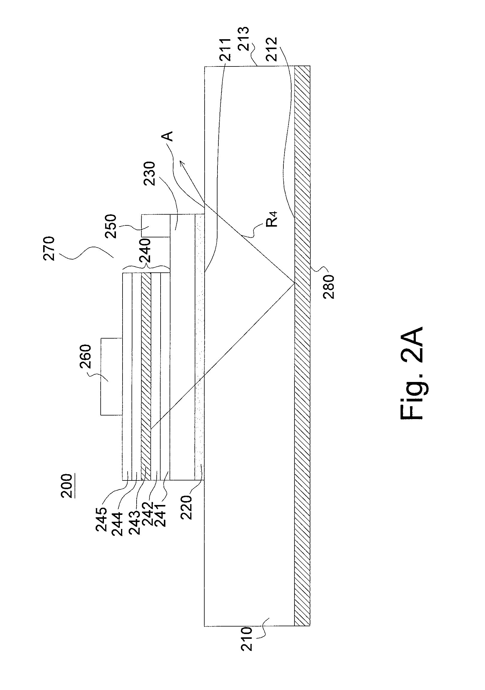
[0017] FIGS. 2A-2C show preferred embodiments of the present invention. A light-emitting device 200 according to the present invention includes a transparent substrate 210, a transparent adhesive layer 220 on the transparent substrate 210, and a first transparent conductive layer 230 on the transparent adhesive layer 220. The material of the transparent substrate 210 includes but not limited to glass, sapphire, SiC, GaP, GaAsP, and ZnSe. The transparent adhesive layer 220 can have a material including but not limited to spin-on glasses, silicone, Benzocyclobutene (BCB), Epoxy, polyimide, and Perfluorocyclobutane (PFCB). The first transparent conductive layer 230 can be made of a material including but not limited to indium tin oxide, cadmium tin oxide, zinc oxide, and zinc tin oxide.
[0018] Moreover, as shown in FIGS. 2A-2C, the light-emitting device 200 according to the present invention further includes a multi-layer epitaxial structure 240 and a first electrode 250 on the first transparent conductive layer 230, and a second electrode 260 on the multi-layer epitaxial structure 240. A trench 270 may be optionally formed between the first electrode 250 and the multi-layer epitaxial structure 240. The multi-layer epitaxial structure 240 includes a first contact layer 241, a first confinement layer 242, a light-emitting layer 243, a second confinement layer 244, and a second contact layer 245. To form a good ohmic contact with the second electrode 260, a second transparent conductive layer 261 capable of spreading currents may be optionally formed between the second electrode 260 and the second contact layer 245. The second transparent conductive layer 261 can be made of a material including but not limited to indium tin oxide, cadmium tin oxide, zinc oxide, and zinc tin oxide. The first contact layer 241 and the second contact layer 245 can be independently made of materials including but not limited to GaP, GaAs, and GaAsP. The first confinement layer 242, the first light-emitting layer 243, and the second confinement layer 244 can be made of materials including AlGaInP. The first electrode 250 and the second electrode 260 can be respectively made of a material including but not limited to Au, Al, Pt, Cr, and Ti. In the structures shown in FIGS. 2A-2C, the transparent substrate 210 has a first surface 211 contacting with the transparent adhesive layer 220 and a second surface 212 opposite to the first surface 211. However, it should be noticed that, the area of the second surface 212 is larger than that of the light-emitting layer 243.
[0019] In the exemplary embodiment of FIG. 2A, the area of the second surface 212 is larger than that of the light-emitting layer 243. As shown in FIG. 2A, the second surface 212 of the transparent substrate has an area essentially equal to that of the first surface 211, and the areas of the first surface 211 and the second surface 212 are larger than the area of the light-emitting layer 243. Therefore, the first surface 211 of the transparent substrate would form an exposed portion, "A", not covered with the light-emitting layer 243. The exposed portion, "A", should at least not be covered with the light-emitting layer 243. For example, the exposed portion, "A", in the figure is not covered with the multi-layer epitaxial structure 240, the first transparent conductive layer 230, and the transparent adhesive layer 220. The size of the exposed portion "A" can be decided upon the area ratio of the first surface 211 to the light-emitting layer 243, the second surface 212 to the light-emitting layer 243, or both of them, and a preferred area ratio is not less than 1.6. The structure having the exposed portion, "A", can increase the brightness of the light-emitting device 200. As shown in FIG. 2A, the light R4 traveling from the second surface 212 upward to the transparent substrate 210 leaves the light-emitting device 200 through the exposed portion, "A", without passing through the light-emitting layer 243, hence the brightness is increased.
[0020] In another exemplary embodiment of FIG. 2B, the area of the second surface 212 is larger than that of the light-emitting layer 243. As shown in the FIG. 2B, the area of the second surface 212 is greater than that of the first surface 211. More specifically, the cross-section of the transparent substrate 210 is like a trapezoid. This structure can increase the brightness of the light-emitting device 200, because the incident angle S2 of the light Rs traveling from the second surface 212 to a side 213 of the transparent substrate 210 is smaller than the critical angle Sc. In detail, a shown in FIG. 2B is the angle that the side 213 tilts to the multi-layer epitaxial structure 240. The angle, "a", changes the incident angle S2 of the light Rs from S1 in FIG. 1B to S2 (namely S2=S1-a), and makes it smaller the critical angle Sc. Consequently, the light Rs leaves the transparent substrate 210 through the side 213, rather than be reflected back into the multi-layer epitaxial structure 240. Those who are skilled in the art should understand that the critical angle Sc mentioned above depends on the material of the transparent substrate 210 and the environmental medium. Therefore, if the environmental medium is set, Sc can be determined by choosing an suitable transparent substrate 210, and the tilt angle, "a" is adjusted by changing the ratio of the area of the second surface 212 to the area of the first surface 211 of the transparent substrate 210. Taking the transparent sapphire substrate 210 for example, the ratio of the area of the second surface 212 to that of the first surface 211 is not less than 1.6, and preferably ranges between 4 and 20. The thickness of the transparent substrate 210 is preferably between 50 to 200 microns, more preferably between 80 to 150 microns.
[0021] In a further exemplary embodiment of FIG. 2C, the area of the second surface 212 is larger than that of the light-emitting layer 243. In this embodiment, the second surface 212 is larger than the first surface 211, and the first surface 211 has an exposed portion, "A". The ratio of the second surface 212 to the first surface 211 and the ratio of the second surface 212 to the light-emitting layer 243 are similar to those mentioned above.
[0022] Additionally, the light-emitting device 200 may further include a reflective layer 280 on the second surface 212 of the transparent substrate 210 in view of demand. The reflective layer 280 shown in FIGS. 2A-2C is, but not limited to, attached directly to the second surface 212. The reflective layer 280 can be made of a material including but not limited to Sn, Al, Au, Pt, An, Ge, Ag and the like. The reflective layer 280 can also be a distributed Bragg reflector (DBR) consisting of oxides, and the oxides can be Ab03, Si02, or Ti02.
[0023] FIGS. 3-7 show preferred embodiments of forming the light emitting devices according to the present invention.
[0024] As shown in FIG. 3, a temporary substrate 310 is provided, and a multi-layer epitaxial structure 240 is formed on the temporary substrate 310. The steps of forming the multi-layer epitaxial structure 240 includes sequentially forming a second contact layer 245, a second confinement layer 244, a light-emitting layer 243, a first confinement layer 242, and a first contact layer 241 on the temporary substrate 310. Then a first transparent conductive layer 230 covering the multi-layer epitaxial structure 240 is formed. As shown in FIG. 3, an etch stop layer 320 is provided between the multi-layer epitaxial structure 240 and temporary substrate 310 to prevent the multi-layer epitaxial structure 240 from damages caused by over etching in subsequent removal of the temporary substrate 310. Preferably, the etch stop layer 320 has an etching rate lower than that of the temporary substrate 310.
[0025] After forming the multi-layer epitaxial structure 240 and the first transparent conductive layer 230 on the temporary substrate 310, the temporary substrate 310 is cut to form a plurality of first dices 400. As shown in FIG. 4, the first dice 400 includes a portion of the multi-layer epitaxial structure 240, a portion of the first transparent conductive layer 230, and a portion of the temporary substrate 310. The cutting step can be performed by use of a diamond tool or a laser tool.
[0026] Then, as shown in FIG. 5, the first dice 400 is attached to the transparent substrate 210. A transparent adhesive layer 220 is formed in advance on the first surface 211 of the transparent substrate 210 for bonding the first dice 400 to the transparent substrate 210. Moreover, a reflective layer 280 may be optionally disposed on the second surface 212 of the transparent substrate 210. The material of the reflective layer 280 is similar to those mentioned above.
[0027] Subsequently, as shown in FIG. 6, the surplus transparent adhesive layer 220 exposed on the transparent substrate 210 is removed, and the temporary substrate 310 is then removed. If the temporary substrate 310 is made of GaAs, it can be removed by a chemical etchant solution such as 5H.sub.3P0.sub.3:3H.sub.20.sub.2:3H.sub.20 or NH.sub.40H:35H.sub.20.sub.2. After removing the temporary substrate 310, the etch stop layer 320 is further removed.
[0028] Then, structures as shown in FIGS. 7A-7C can be formed by conventional processes, such as deposition, lithography and etching. In detail, the multi-layer epitaxial structure 240 is selectively etched to expose the underlying first transparent conductive layer 230. Subsequently, a trench 270 as shown in FIGS. 7A-7C is formed, a first electrode 250 is formed on the first transparent conductive layer 230, and a second electrode 260 is formed on the multi-layer epitaxial structure 240. The trench 270 isolates the multi-layer epitaxial structure 240 from the first electrode 250. The first electrode 250 and the second electrode 260 are formed on the same side of the transparent substrate 210. Additionally, a second transparent conductive layer 261 capable of spreading currents may be optionally formed between the second electrode 260 and the second contact layer 245. The second transparent conductive layer 261 forms a good ohmic contact with the second electrode 260. The second transparent conductive layer 261 can be made of a material of the first transparent conductive layer 230 as mentioned above.
[0029] Next, the transparent substrate 210 is cut to form a plurality of second dice 200 (namely the light-emitting devices 200). The dotted lines in FIGS. 7A-7C respectively illustrate different cutting manners for obtaining the light-emitting devices 200 shown in FIGS. 2A-2C. After cutting, the second dice 200 includes the first dice 400, a portion of the transparent adhesive layer 220, and a portion of the transparent substrate 210. During cutting, it should be noticed that, the transparent substrate 210 of thus formed second dice 200 has a first surface 211 contacting with the transparent adhesive layer 220 and a second surface 212 opposite to the first surface 211, and the area of the second surface 212 is larger than that of the light-emitting layer 243. The cutting manner of FIG. 7A exposes a portion, "A", of the transparent substrate 210 of the second dice 200. The cutting manner of FIG. 7B makes the second surface 212 of the transparent substrate 210 of the second dice 200 be larger than the first surface 211 without the portion, "A". The cutting manner of FIG. 7C creates the feature that the second surface 212 of the transparent substrate 210 of the second dice 200 is larger than the first surface 211 with the portion, "A". The cutting can be performed by wafer dicing equipments with a diamond tool or a laser tool. To reduce the heat produced by cutting and take away the debris, water with a constant amount at a given pressure may be laterally introduced along the rotating direction of the diamond tool during the cutting step.
[0030] The detailed description of the above preferred embodiments is to describe the features and spirit of the present invention more clearly, and is not intended to limit the scope of the present invention. The scope of the present invention should be most broadly explained according to the foregoing description and includes all possible variations and equivalents.
* * * * *
D00000
D00001
D00002
D00003
D00004
D00005
D00006
D00007
D00008
XML
uspto.report is an independent third-party trademark research tool that is not affiliated, endorsed, or sponsored by the United States Patent and Trademark Office (USPTO) or any other governmental organization. The information provided by uspto.report is based on publicly available data at the time of writing and is intended for informational purposes only.
While we strive to provide accurate and up-to-date information, we do not guarantee the accuracy, completeness, reliability, or suitability of the information displayed on this site. The use of this site is at your own risk. Any reliance you place on such information is therefore strictly at your own risk.
All official trademark data, including owner information, should be verified by visiting the official USPTO website at www.uspto.gov. This site is not intended to replace professional legal advice and should not be used as a substitute for consulting with a legal professional who is knowledgeable about trademark law.