Plasma Processing Apparatus And Method For Forming Semiconductor Device Structure
CHEN; Po-Ju ; et al.
U.S. patent application number 16/104564 was filed with the patent office on 2019-05-23 for plasma processing apparatus and method for forming semiconductor device structure. This patent application is currently assigned to Taiwan Semiconductor Manufacturing Co., Ltd.. The applicant listed for this patent is Taiwan Semiconductor Manufacturing Co., Ltd.. Invention is credited to Chih-Hao CHEN, Po-Ju CHEN, Yi-Wei CHIU, Chun-Hsing WU, Fang-Yi WU.
| Application Number | 20190157048 16/104564 |
| Document ID | / |
| Family ID | 66533298 |
| Filed Date | 2019-05-23 |


View All Diagrams
| United States Patent Application | 20190157048 |
| Kind Code | A1 |
| CHEN; Po-Ju ; et al. | May 23, 2019 |
PLASMA PROCESSING APPARATUS AND METHOD FOR FORMING SEMICONDUCTOR DEVICE STRUCTURE
Abstract
A plasma processing apparatus is provided. The plasma processing apparatus includes a plasma chamber including a housing, and a first electrode array disposed above and outside the housing. The first electrode array includes a plurality of first sub-electrodes. The plasma processing apparatus also includes a number of first matching units outside of the housing, and each of the first matching units is electrically connected to each of the first sub-electrodes.
| Inventors: | CHEN; Po-Ju; (Hsinchu City, TW) ; WU; Chun-Hsing; (Zhubei City, TW) ; WU; Fang-Yi; (Kaohsiung City, TW) ; CHIU; Yi-Wei; (Kaohsiung City, TW) ; CHEN; Chih-Hao; (Hsinchu City, TW) | ||||||||||
| Applicant: |
|
||||||||||
|---|---|---|---|---|---|---|---|---|---|---|---|
| Assignee: | Taiwan Semiconductor Manufacturing
Co., Ltd. Hsinchu TW |
||||||||||
| Family ID: | 66533298 | ||||||||||
| Appl. No.: | 16/104564 | ||||||||||
| Filed: | August 17, 2018 |
Related U.S. Patent Documents
| Application Number | Filing Date | Patent Number | ||
|---|---|---|---|---|
| 62587751 | Nov 17, 2017 | |||
| Current U.S. Class: | 1/1 |
| Current CPC Class: | H01L 21/67103 20130101; H01J 37/32568 20130101; H01L 21/3065 20130101; H01J 37/32541 20130101; H01L 21/6831 20130101; H01L 21/768 20130101; H01L 29/66795 20130101; H01L 21/76816 20130101; H01J 37/32715 20130101; H01L 21/67069 20130101; H01J 37/3255 20130101; H01J 37/32183 20130101; H01J 2237/334 20130101; H01L 21/31116 20130101; H01L 21/6833 20130101 |
| International Class: | H01J 37/32 20060101 H01J037/32; H01L 21/67 20060101 H01L021/67; H01L 21/683 20060101 H01L021/683; H01L 21/3065 20060101 H01L021/3065 |
Claims
1. A plasma processing apparatus, comprising: a plasma chamber comprising a housing and a wafer support; a first electrode array disposed over the wafer support, wherein the first electrode array comprises a plurality of first sub-electrodes; and a plurality of first matching units connected to the first electrode array, wherein each of the first matching units is electrically connected to each of the first sub-electrodes.
2. The plasma processing apparatus as claimed in claim 1, further comprising: a first RF power source connected to the plurality of first sub-electrodes configured to provide energy to the plurality of first sub-electrodes via the plurality of first matching units.
3. The plasma processing apparatus as claimed in claim 1, further comprising: a wafer support disposed in the plasma chamber; and a second electrode array disposed in the wafer support, wherein the second electrode array comprises a plurality of second sub-second electrodes.
4. The plasma processing apparatus as claimed in claim 3, further comprising: a plurality of second matching units connected to the plurality of second sub-electrodes, wherein each of the second matching units is electrically connected to one of the plurality of second sub-electrodes.
5. The plasma processing apparatus as claimed in claim 4, further comprising: a second RF power source connected to the plurality of second sub-electrodes configured to provide energy to the plurality of second sub-electrodes via the plurality of second matching units.
6. The plasma processing apparatus as claimed in claim 3, wherein each of the plurality of first sub-electrodes and the plurality of second sub-electrodes comprises aluminum (Al), nickel (Ni), chromium (Cr), tin (Sn), copper (Cu), platinum (Pt), gold (Au), ceramic or piezoelectric material.
7. The plasma processing apparatus as claimed in claim 1, wherein each of the first sub-electrodes has a distance which is measured from a top surface of the housing to a bottom surface of each of the plurality of first sub-electrodes, and the first sub-electrodes have the same or different heights.
8. The plasma processing apparatus as claimed in claim 1, wherein the first electrode array further comprises an insulating material insulates the adjacent sidewalls of the plurality of first sub-electrodes.
9. The plasma processing apparatus as claimed in claim 1, wherein the plurality of first sub-electrodes is arranged in a spiral shape when seen from a top-view.
10. The plasma processing apparatus as claimed in claim 1, further comprising: a plurality of gas channels disposed in the wafer support, wherein the gas channels are disposed above the second electrode array; an electrostatic electrode disposed in the wafer support; and a cooling plate disposed in the wafer support, wherein the electrostatic electrode is between the gas channels and the cooling plate.
11. A plasma processing apparatus, comprising: a plasma chamber comprising a housing and a wafer support; a top electrode array disposed over the wafer support, wherein the top electrode array comprises a plurality of top sub-electrodes spaced apart from one another; and a bottom electrode array disposed in the wafer support, wherein the bottom electrode comprises a plurality of bottom sub-electrodes spaced apart from one another.
12. The plasma processing apparatus as claimed in claim 11, further comprising: a plurality of top matching units each electrically connected to one of the plurality of top sub-electrodes; and a first RF power source configured to provide energy to the top sub-electrodes via the plurality of top matching units.
13. The plasma processing apparatus as claimed in claim 11, further comprising: a plurality of gas channels disposed in the wafer support, wherein the plurality of gas channels is positioned above the bottom electrode array; and an electrostatic electrode disposed in the wafer support, wherein the electrostatic electrode is positioned above the bottom electrode array.
14. The plasma processing apparatus as claimed in claim 13, further comprising: a plurality of bottom matching units each electrically connected to one of the plurality of bottom sub-electrodes.
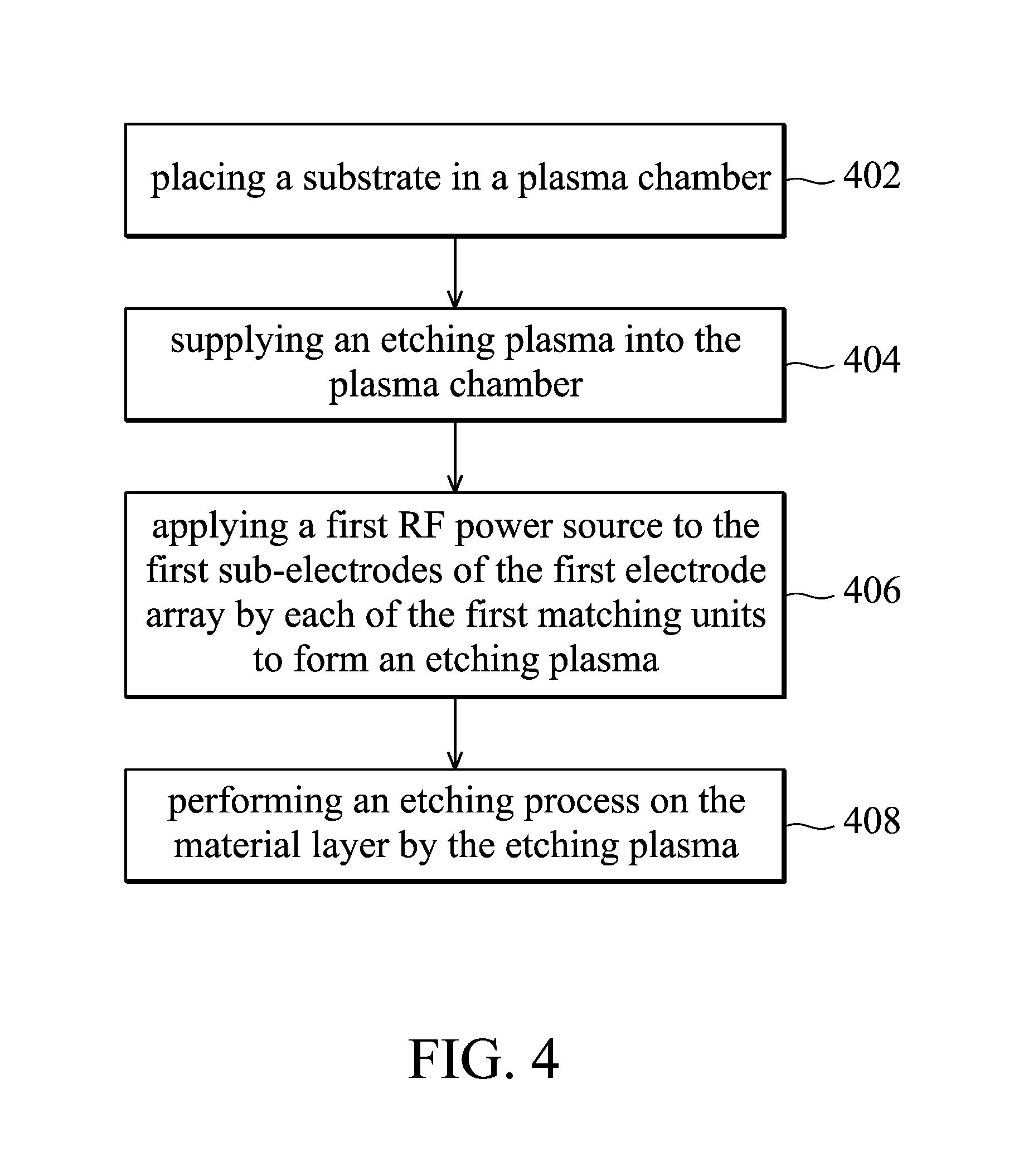
15. The plasma processing apparatus as claimed in claim 11, wherein two adjacent ones of the plurality of top sub-electrodes are separated from each other by a dielectric layer.
16. The plasma processing apparatus as claimed in claim 11, wherein the top electrode array further comprises an insulating material insulates the adjacent sidewalls of the top sub-electrodes.
17. A method for forming a semiconductor device structure, comprising: placing in a plasma chamber a substrate including a material layer thereon, wherein the plasma chamber comprises: a housing; a first electrode array comprising a plurality of first sub-electrodes; a plurality of first matching units each electrically connected to one of the plurality of first sub-electrodes; and a second electrode array disposed in the housing, the second electrode array comprising a plurality of second sub-electrodes; supplying an etching gas into the plasma chamber; applying a first RF power source to the first sub-electrodes of the first electrode array by each of the first matching units to form an etching plasma from the etching gas, adjusting a distance between each of the first sub-electrodes and the substrate to generate a plasma density distribution across the substrate; and performing an etching process on the material layer using the etching plasma.
18. The method of claim 17, further comprising: applying a second RF power source to the plurality of second sub-electrodes of the second electrode array by a plurality of second matching units, wherein the plurality of second sub-electrodes is configured to increase the plasma density near the material layer.
19. The method of claim 18, further comprising: supplying a cleaning gas into the plasma chamber; performing a cleaning process on an edge region of the substrate by applying the first RF power source to a portion of the plurality of first sub-electrodes which is located at an edge region of the first electrode array to increase the plasma density near the edge region of the substrate.
20. The method of claim 17, wherein the etching plasma has different plasma density in different regions above the substrate.
Description
CROSS REFERENCE TO RELATED APPLICATIONS
[0001] This Application claims the benefit of U.S. Provisional Application No. 62/587,751, filed on Nov. 17, 2017, and entitled "Plasma processing apparatus and method for forming semiconductor device structure", the entirety of which is incorporated by reference herein.
BACKGROUND
[0002] Semiconductor devices are used in a variety of electronic applications, such as personal computers, cell phones, digital cameras, and other electronic equipment. Semiconductor devices are typically fabricated by sequentially depositing insulating or dielectric layers, conductive layers, and semiconductive layers of material over a semiconductor substrate, and patterning the various material layers using lithography to form circuit components and elements thereon. Many integrated circuits are typically manufactured on a single semiconductor wafer, and individual dies on the wafer are singulated by sawing between the integrated circuits along a scribe line. The individual dies are typically packaged separately, in multi-chip modules, for example, or in other types of packaging.
[0003] A plasma processing (dry etching) process offers better critical dimension control than conventional wet chemical etching in the fabrication of semiconductor devices.
[0004] Although existing plasma processing apparatuses have generally been adequate for their intended purpose, they have not been entirely satisfactory in all respects.
BRIEF DESCRIPTION OF THE DRAWINGS
[0005] Aspects of the present disclosure are best understood from the following detailed description when read with the accompanying figures. It should be noted that, in accordance with the standard practice in the industry, various features are not drawn to scale. In fact, the dimensions of the various features may be arbitrarily increased or reduced for clarity of discussion.
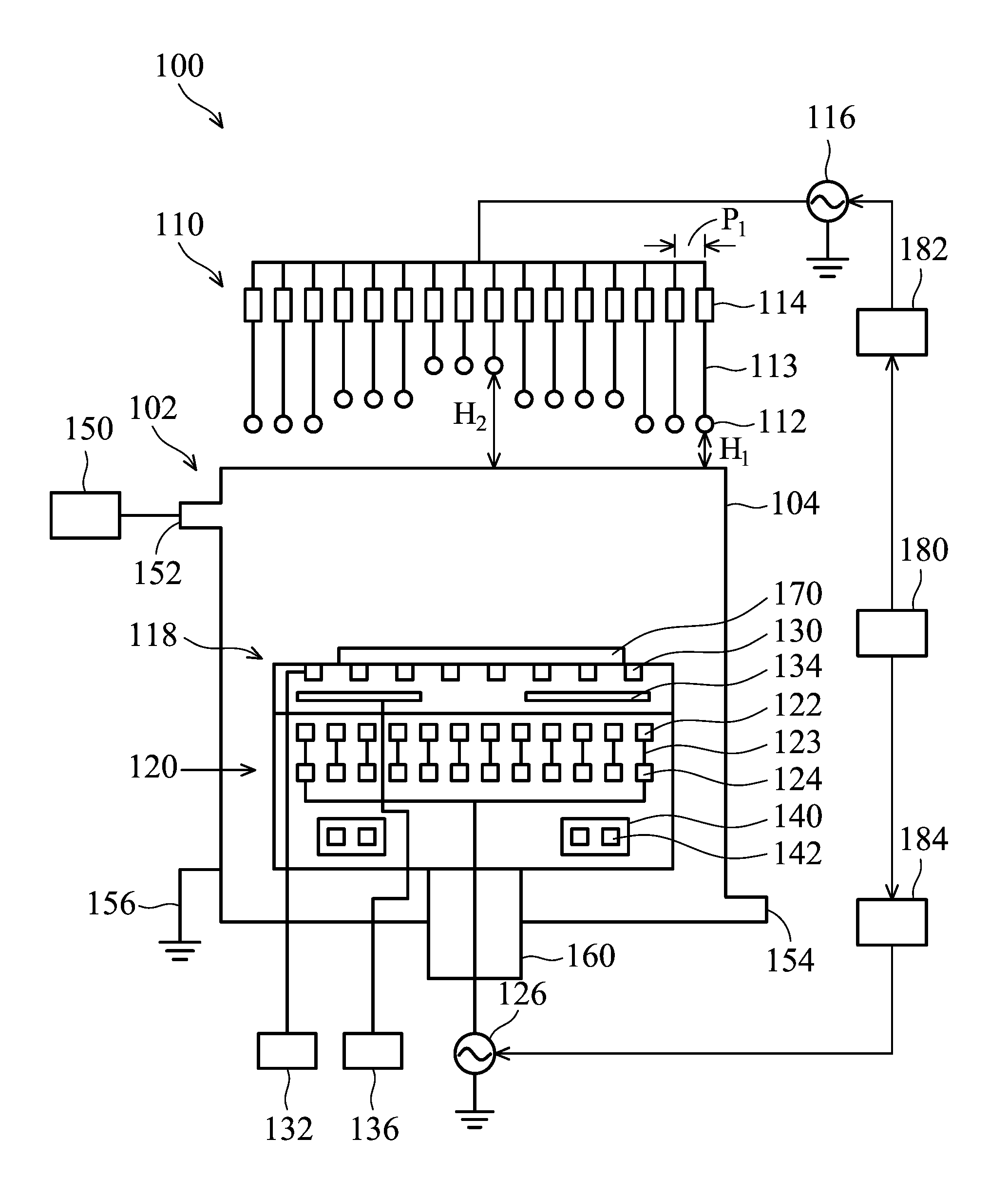
[0006] FIG. 1 shows a schematic view of a plasma processing apparatus, in accordance with some embodiments of the disclosure.
[0007] FIG. 2A shows a top-view of the first sub-electrodes, in accordance with some embodiments of the disclosure.
[0008] FIG. 2A' shows a top-view of the first sub-electrodes, in accordance with some embodiments of the disclosure.
[0009] FIGS. 2B and 2B' show top-views of the first sub-electrodes in accordance with some embodiments of the disclosure.
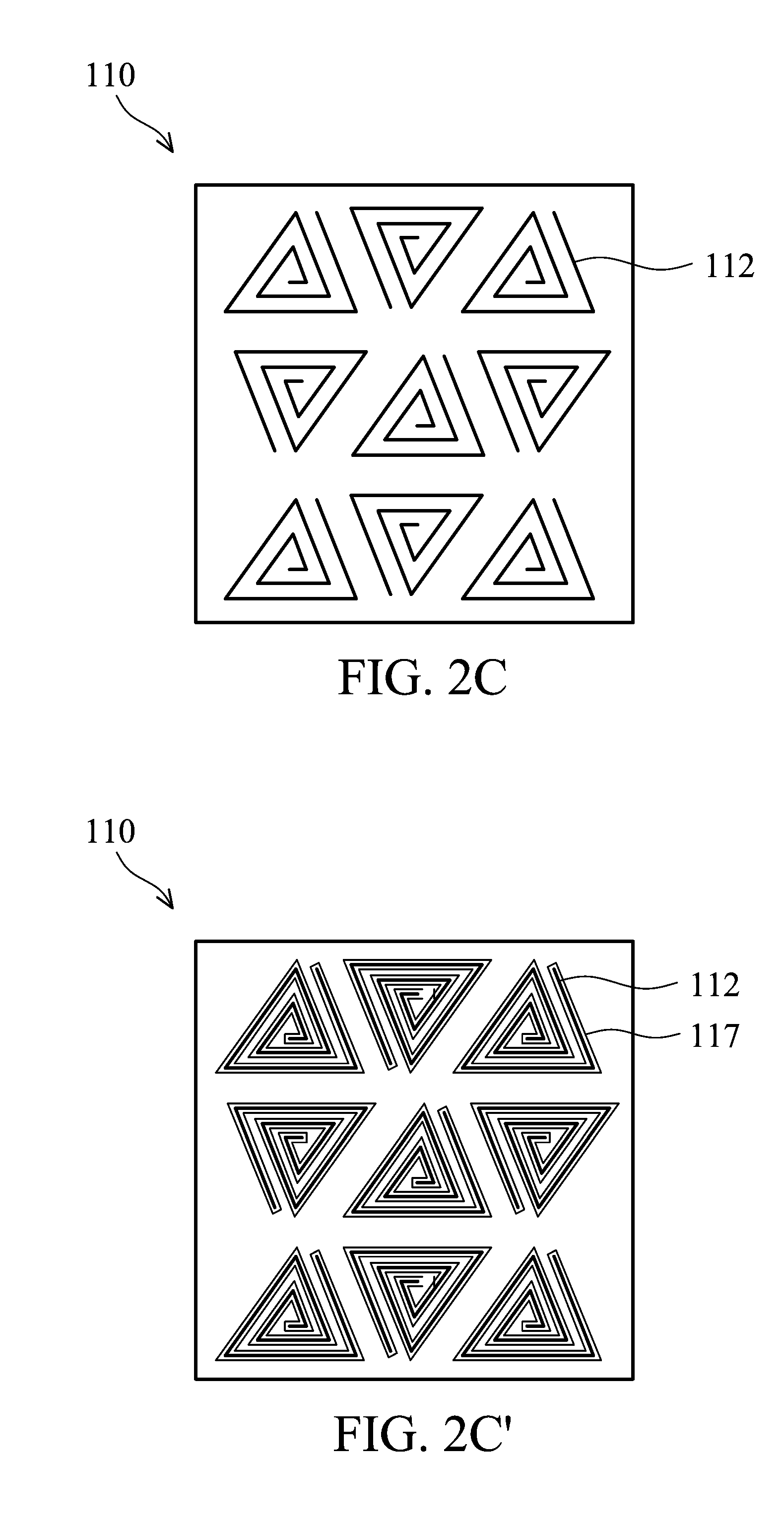
[0010] FIGS. 2C and 2C' show top-views of the first sub-electrodes, in accordance with some embodiments of the disclosure.
[0011] FIGS. 2D and 2D' show top-views of the first sub-electrodes, in accordance with some embodiments of the disclosure.
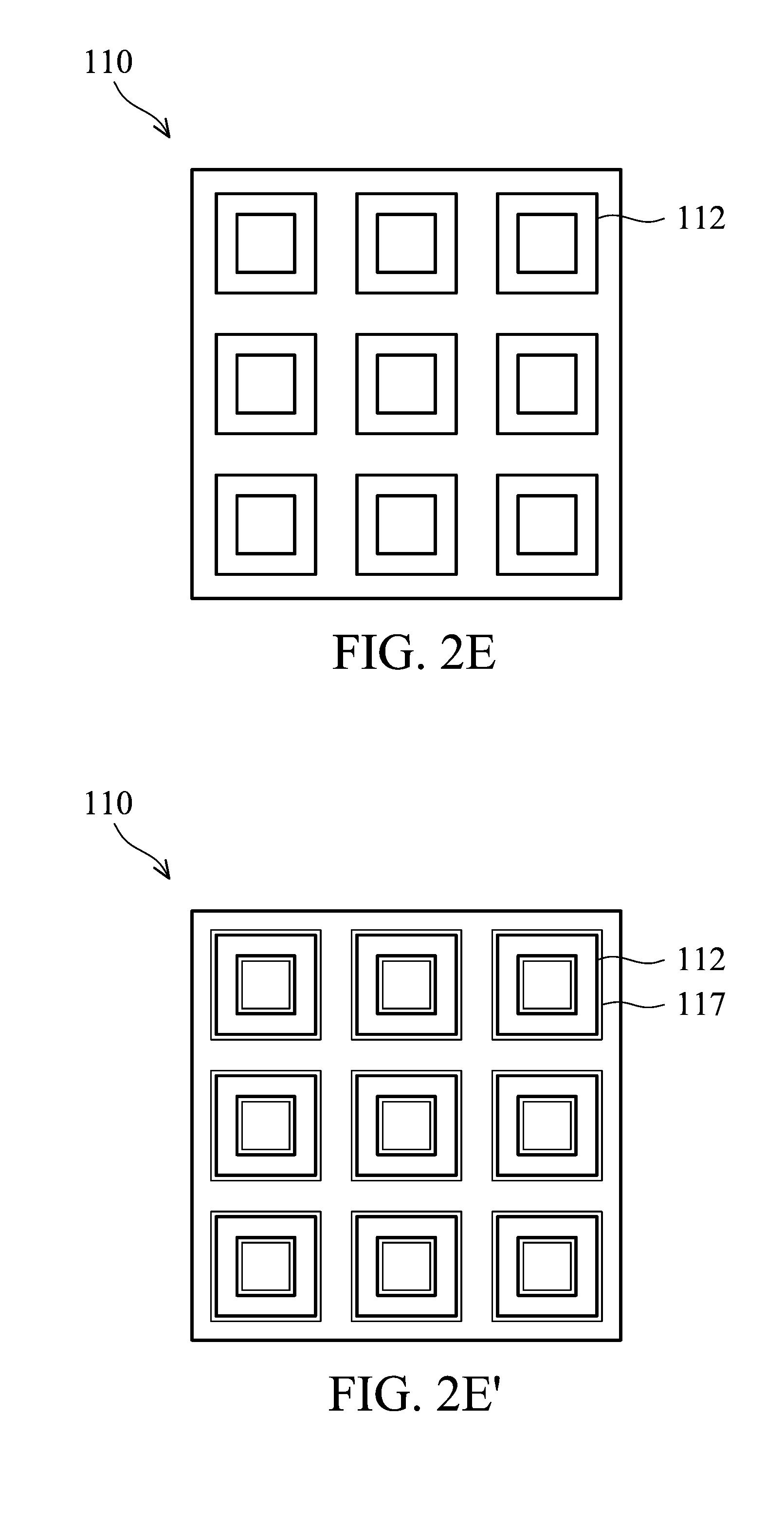
[0012] FIGS. 2E and 2E' show top-views of the first sub-electrodes, in accordance with some embodiments of the disclosure.
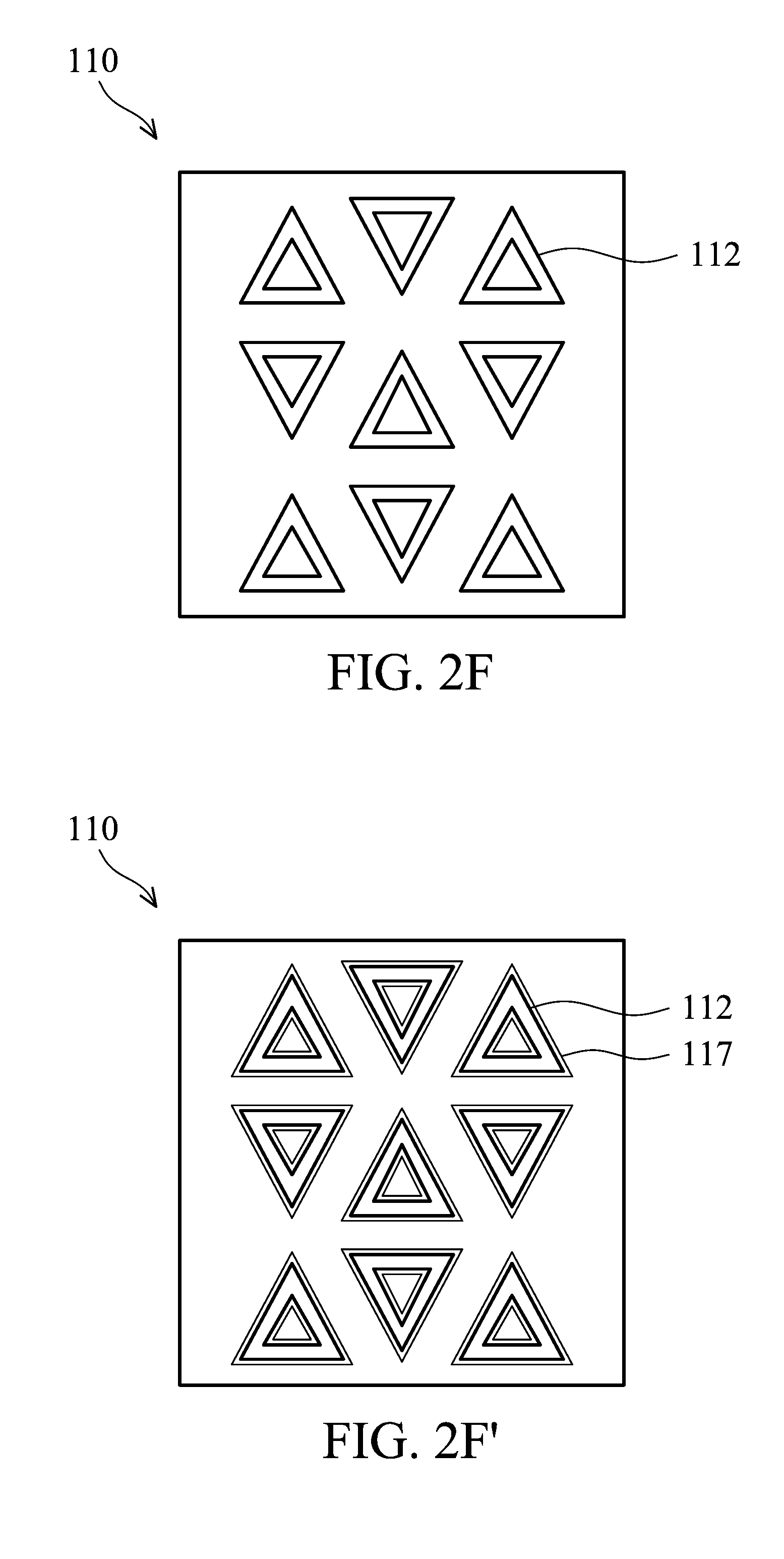
[0013] FIGS. 2F and 2F' show top-views of the first sub-electrodes, in accordance with some embodiments of the disclosure.
[0014] FIGS. 3A-3C shows top-views of the second sub-electrodes, in accordance with some embodiments of the disclosure.
[0015] FIG. 4 shows a flow-chart of a method for forming a semiconductor device structure, in accordance with some embodiments.
[0016] FIGS. 5A-5C show cross-sectional views of various stages of forming a semiconductor device structure, in accordance with some embodiments of the disclosure.
[0017] FIGS. 6A-6C show cross-sectional views of various stages of forming a semiconductor device structure, in accordance with some embodiments of the disclosure.
[0018] FIGS. 7A-7E show cross-sectional views of various stages of forming a semiconductor device structure, in accordance with some embodiments of the disclosure.
DETAILED DESCRIPTION
[0019] The following disclosure provides many different embodiments, or examples, for implementing different features of the subject matter provided. Specific examples of components and arrangements are described below to simplify the present disclosure. These are, of course, merely examples and are not intended to be limiting. For example, the formation of a first feature over or on a second feature in the description that follows may include embodiments in which the first and second features are formed in direct contact, and may also include embodiments in which additional features may be formed between the first and second features, such that the first and second features may not be in direct contact. In addition, the present disclosure may repeat reference numerals and/or letters in the various examples. This repetition is for the purpose of simplicity and clarity and does not in itself dictate a relationship between the various embodiments and/or configurations discussed.
[0020] Some variations of the embodiments are described. Throughout the various views and illustrative embodiments, like reference numbers are used to designate like elements. It should be understood that additional operations can be provided before, during, and after the method, and some of the operations described can be replaced or eliminated for other embodiments of the method.
[0021] The fins may be patterned using any suitable method. For example, the fins may be patterned using one or more photolithography processes, including double-patterning or multi-patterning processes. Generally, double-patterning or multi-patterning processes combine photolithography and self-aligned processes, allowing patterns to be created that have, for example, pitches smaller than what is otherwise obtainable using a single, direct photolithography process. For example, in one embodiment, a sacrificial layer is formed over a substrate and patterned using a photolithography process. Spacers are formed alongside the patterned sacrificial layer using a self-alignment process. The sacrificial layer is then removed, and the remaining spacers may then be used to pattern the fins.
[0022] Embodiments for a plasma processing apparatus are provided. FIG. 1 shows a schematic view of a plasma processing apparatus 100, in accordance with some embodiments of the disclosure. The plasma processing apparatus 100 includes a plasma chamber 102, a first electrode array 110 (or top electrode array) and a second electrode array 120 (or bottom electrode array). The plasma chamber 102 includes a housing 104 (or wall portions). The housing 104 is configured to maintain a vacuum environment during processing. The housing 104 is grounded through a ground 156.
[0023] The housing 104 includes a gas inlet 152 and a gas outlet 154. The gas inlet 152 is connected to the plasma chamber 102. A gas supply 150 is coupled to the plasma chamber 102. The gas from the gas supply 150 is supplied to the plasma chamber 102 through the gas inlet 152. The gas supply 150 may supply a single gas or a gas mixture of more than one gas. The gas outlet 154 is connected to the plasma chamber 102. The chemical byproducts and unwanted reagents from the plasma chamber 102 are evacuated via gas outlet 154.
[0024] The first electrode array 110 is disposed above and outside the housing 104. The first electrode array 110 includes a number of first sub-electrodes 112 (or top sub-electrodes). In some embodiments, the first sub-electrodes 112 are made of low-resistivity material. In some embodiments, the first sub-electrodes 112 are made of conductive materials, such as aluminum (Al), nickel (Ni), chromium (Cr), tin (Sn), copper (Cu), platinum (Pt), gold (Au), ceramic or piezoelectric material.
[0025] A number of first matching units 114 are outside the housing 104. The first matching units 114 are used to perform an impedance matching function. Each of the first matching units 114 are electrically connected to corresponding first sub-electrodes 112 by a number of first conductive lines 113. The first conductive lines 113 may have different lengths. Therefore, the first sub-electrodes 112 have different heights H.sub.1, H.sub.2. The heights H.sub.1, H.sub.2 is measured from the top surface of the housing 104 to the bottom surface of each of the first sub-electrodes 112. The plasma density in the plasma chamber 102 can be controlled by adjusting the height H.sub.1, H.sub.2 of each of the first sub-electrodes 112. In some embodiments, a first portion of the first sub-electrodes 112 in the edge region of the first electrode array 110 has a first height H.sub.1, and a second portion of the first sub-electrodes 112 in the middle region of the first electrode array 110 has a second height H.sub.2. The second height H.sub.2 is greater than the first height H.sub.1. When the first portion of the first sub-electrodes 112 is closer to the housing 104 than the second portion of the first sub-electrodes 112, a first plasma density of a first region which is directly below the first portion of the first sub-electrodes 112 will be higher than a second plasma density of a second region which is directly below the second portion of the first sub-electrodes 112. In some embodiments, the first height H.sub.1 is in a range from about 0.1 cm to about 20 cm. There is a first pitch P.sub.1 between two adjacent first sub-electrodes 112. In some embodiments, the first pitch P.sub.1 is in a range from about 0.05 mm to about 10 mm.
[0026] A first RF power source 116 is electrically connected to the number of the first matching units 114. The first RF power source 116 is configured to provide a RF power (or RF energy) to each of the first sub-electrodes 112 via each of the first matching units 114. The first RF power source 116 is configured to supply an RF power for plasma generation to the first sub-electrodes 112 through the first matching units 114. The first matching units 114 are disposed on the transmission path between the first RF power source 116 and the first sub-electrodes 112, and the first matching units 114 are configured to perform an impedance matching function. More specifically, through the help of the number of the first matching units 114, the first RF power source 116 can provide different levels of RF power to the first sub-electrodes 112 to form a desired plasma density distribution in the different regions of the plasma chamber 102.
[0027] The first sub-electrodes 112 are separately controlled by a number of first matching units 114. In some embodiments, the first RF power generated from the first RF power source 116 applies a high-frequency in a range from about 1 MHz to about 100 MHz.
[0028] A wafer support 118 is disposed in the plasma chamber 102. The wafer support 118 is configured to support a wafer or substrate 170. The second electrode array 120 (or bottom electrode array) is disposed in the wafer support 118 in the plasma chamber 102. A number of gas channels 130 are disposed in the wafer support 118. The gas channels 130 are connected to a gas supply 132. The gas channels 130 are configured to transfer the heat to provide uniform temperature distribution. The heat may be generated from the electrostatic electrode 134 or from the etching process. An electrostatic electrode 134 is disposed in the wafer support 118 and is configured to hold the substrate 170 by an electrostatic attracting force. The electrostatic electrode 134 is connected to a chuck power 136.
[0029] The second electrode array 120 includes a number of second sub-electrodes 122 (or bottom sub-electrodes). A number of second matching units 124 are electrically connected to corresponding the second sub-electrodes 122. Each of the second matching units 124 are electrically connected to corresponding second sub-electrodes 122 by a number of second conductive lines 123. In some embodiments, the second sub-electrodes 122 are made of low-resistivity material. In some embodiments, the second sub-electrodes 122 are made of conductive materials, such as aluminum (Al), nickel (Ni), chromium (Cr), tin (Sn), copper (Cu), platinum (Pt), gold (Au), ceramic or piezoelectric material.
[0030] A second RF power source 126 is disposed outside the housing 104 and the plasma chamber 102. The second RF power source 126 is configured to provide a RF power (or RF energy) to each of the second sub-electrodes 122 via each of the second matching units 124. More specifically, the second RF power source 126 is configured to provide different RF powers to the second sub-electrodes 122 through the number of the second matching units 124 to form a desired plasma density distribution in the different regions of the plasma chamber 102. The second sub-electrodes 122 are separately controlled by a number of second matching units 124.
[0031] A cooling plate 140 is disposed in the wafer support 118 to form a built-in cooling mechanism, and a cooling fluid 142 are disposed in the cooling plate 140. The cooling plate 140 is configured to cool the temperature of the substrate 170. A moving mechanism 160 is below the wafer support 118 and enables the wafer support 118 assembly to move up or down.
[0032] A controller 180 is coupled to the plasma chamber 102. The controller 180 sets the operational parameters of the plasma chamber 102, including which RF power sources are turned on or turned off, their voltages and power settings. The controller 180 is coupled to a first power controller 182 and a second power controller 184. The first power controller 182 provides the control signals to the first RF generator 116 to control the amount of power from the first RF generator 116. The second power controller 184 provides the control signals to the second RF generator 126 to control the amount of power from the second RF generator 126. In some embodiments, the controller 180 sends instructions to the first power controller 182 for the configuration of the power on the first sub-electrodes 112, which includes setting switch to connect the first sub-electrodes 112 to ground or to RF power. In some other embodiments, the controller 180 sends instructions to the first power controller 182 and the second power controller 184, which includes switching to connect the first sub-electrodes 112 to ground or to RF power, and switching to connect the second sub-electrodes 122 to ground or to RF power.
[0033] The plasma is generated between the top surface of the plasma chamber 102 and the wafer support 118. For example, the first sub-electrodes 112 are independently or separately powered by the first RF power source 116 through the number of the first matching units 114 to produce inductively coupled plasma (ICP) in the plasma chamber 102. In some embodiments, an electric field is generated by the first RF power source 116 to excite the reaction gas into the plasma chamber 102 while the etching gas or the cleaning gas is supplied into the plasma chamber 102 via the gas inlet 152. Afterwards, the reaction gas is excited into plasma by the electric field. After generation the plasma, the material layer 506 (shown in FIG. 5B) is etched by the plasma.
[0034] In some embodiments, the etching gas is supplied by the gas supply 150 into the plasma chamber 102. The etching gas includes fluorine-containing gas that includes nitrogen trifluoride (NF.sub.3), hexafluoroethane (C.sub.2F.sub.6), tetrafluoromethane (CF.sub.4), fluoroform (CHF.sub.3), fluorine (F.sub.2), hydrogen fluoride (HF), or a combination thereof. In some other embodiments, the etching gas further includes another additive gas, such as oxygen (O.sub.2) or ozone (O.sub.3).
[0035] In some embodiments, the cleaning gas is supplied by the gas supply 150 into the plasma chamber 102. The cleaning gas includes fluorine-containing gas, inert gas, or a combination thereof. The fluorine-containing gas includes nitrogen trifluoride (NF.sub.3), hexafluoroethane (C.sub.2F.sub.6), tetrafluoromethane (CF.sub.4), fluoroform (CHF.sub.3), fluorine (F.sub.2), hydrogen fluoride (HF), or a combination thereof. The inert gas includes argon (Ar), helium (He), neon (Ne), krypton (Kr), xenon (Xe), or a combination thereof.
[0036] FIG. 2A shows a top-view of the first sub-electrodes 112, in accordance with some embodiments of the disclosure.
[0037] The first sub-electrodes 112 include a number of parts. In some embodiments, the first sub-electrodes 112 include a first part 112a, a second part 112b, a third part 112c, a fourth part 112d, a fifth part 112e, a sixth part 112f, a seventh part 112g, an eighth part 112h and a ninth part 112i. These parts 112a, 112b, 112c, 112d, 112e, 112f, 112g, 112h, 112i are separate from each other and arranged in a matrix. The first sub-electrodes 112 are separated from each other by a dielectric layer 115 between two adjacent first sub-electrodes 112. In some embodiments, each of the first sub-electrodes 112 has a spiral shape when seen from a top-view. In some embodiments, each of the parts of the first sub-electrodes 112 has a size in a range from about 0.1 cm.sup.2 to about 1 cm.sub.2.
[0038] FIG. 2A' shows a top-view of the first sub-electrodes 112, in accordance with some embodiments of the disclosure. FIG. 2A' is similar to FIG. 2A, the difference being that the adjacent sidewalls of the parts 112a, 112b, 112c, 112d, 112e, 112f, 112g, 112h, 112i of the first sub-electrodes 112 in FIG. 2A' are insulated by the insulating material 117.
[0039] FIGS. 2B and 2B' show top-views of the first sub-electrodes 112 in accordance with some embodiments of the disclosure. Each of the first sub-electrodes 112 has a squared spiral shape when seen from a top-view. FIG. 2B' is similar to FIG. 2B, with the difference between them being the insulating material 117 that covers the outer surface of each of the first sub-electrodes 112.
[0040] FIGS. 2C and 2C' show top-views of the first sub-electrodes 112, in accordance with some embodiments of the disclosure. Each of the first sub-electrodes 112 has a triangular spiral shape when seen from a top-view. FIG. 2C' is similar to FIG. 2C, the difference between them being that an insulating material 117 covers the outer surface of each of the first sub-electrodes 112.
[0041] FIGS. 2D and 2D' show top-views of the first sub-electrodes 112, in accordance with some embodiments of the disclosure. Each of the first sub-electrodes 112 has a concentric ring shape when seen from a top-view. FIG. 2D' is similar to FIG. 2D, the difference between is that an insulating material 117 is covering the outer surface of each of the first sub-electrodes 112.
[0042] FIGS. 2E and 2E' show top-views of the first sub-electrodes 112, in accordance with some embodiments of the disclosure. Each of the first sub-electrodes 112 has a rectangular concentric shape when seen from a top-view. FIG. 2E' is similar to FIG. 2E, the difference between is that an insulating material 117 covers the outer surface of each of the first sub-electrodes 112.
[0043] FIGS. 2F and 2F' show top-views of the first sub-electrodes 112, in accordance with some embodiments of the disclosure. Each of the first sub-electrodes 112 has a triangular concentric shape when seen from a top-view. FIG. 2F' is similar to FIG. 2F, the difference between them being that there is an insulating material 117 covering the outer surface of each of the first sub-electrodes 112.
[0044] It should be noted that the number of first sub-electrodes 112 is not limited to nine, and that the number of first sub-electrodes 112 can be adjusted according to actual application.
[0045] FIGS. 3A-3C show top-views of the second sub-electrodes 122, in accordance with some embodiments of the disclosure. The second sub-electrodes 122 include a number of parts. In some embodiments, the second sub-electrodes 122 include a first part 122a, a second part 122b, a third part 122c, a fourth part 122d, a fifth part 122e, a sixth part 122f, a seventh part 122g, an eighth part 122h and a ninth part 122i. These parts 122a, 122b, 122c, 122d, 122e, 122f, 122g, 122h, 122i are separate from each other and arranged in a matrix. The second sub-electrodes 122 are separated from each other by a dielectric layer 125 between two adjacent second sub-electrodes 122. In FIG. 3A, each of the second sub-electrodes 122 has a circular shape when seen from a top-view.
[0046] In FIG. 3B, each of the second sub-electrodes 122 has a rectangular shape when seen from a top-view. In FIG. 3C, each of the second sub-electrodes 122 has a triangular shape when seen from a top-view.
[0047] FIG. 4 shows a flow-chart of a method for forming a semiconductor device structure, in accordance with some embodiments.
[0048] In operation 402, the substrate 170 as shown in FIG. 1 is placed in the plasma chamber 102. In some embodiments, a material layer 506 (as shown in FIG. 5A) is formed over the substrate 502.
[0049] In operation 404, an etching gas is supplied into the plasma chamber 102. In some embodiments, the etching gas includes fluorine-containing gas that includes nitrogen trifluoride (NF.sub.3), hexafluoroethane (C.sub.2F.sub.6), tetrafluoromethane (CF.sub.4), fluoroform (CHF.sub.3), fluorine (F.sub.2), hydrogen fluoride (HF), or a combination thereof. In some other embodiments, the etching gas further includes another additive gas, such as oxygen (O.sub.2) or ozone (O.sub.3).
[0050] In operation 406, a first RF power source 116 is applied to the first sub-electrodes 112 of the first electrode array 110 by each of the first matching units 114 to produce an etching plasma. Therefore, the process gas supplied in the plasma chamber 102 is excited and dissociated to form a plasma. In some embodiments, the etching plasma has different plasma densities in different regions above the substrate 170 or 502 by applying a different levels of RF power to every first sub-electrode 112. In some embodiments, the density of the plasma in the central region is increased by increasing the RF power of the corresponding first sub-electrode 112 in the central region.
[0051] In some other embodiments, a second RF power source 126 is applied to the second sub-electrodes 122 of the second electrode array 120. Therefore, an etchant or the etching plasma in the plasma chamber 102 is guided onto a surface of the substrate 170.
[0052] It should be noted that the first RF power source 116 and the second RF power source 126 are controlled separately to obtain stable plasma. The plasma in the housing 104 is controlled by the first RF power source 116, and the bombardment is controlled by the second RF power source 126. In some embodiments, only the first RF power source 116 is operated. For example, when a photoresist layer is removed, only the first RF power source 116 is operated. In some other embodiments, the first RF power source 116 and the second RF power source 126 are operated simultaneously using the controller 180. For example, when substrate 102 is made of silicon (Si), the first RF power source 116 and the second RF power source 126 are operated simultaneously in the etching process. The first RF power source 116 is used to remove the silicon material and the second RF power source 126 is used to remove the silicon oxide formed over the silicon.
[0053] In operation 408, an etching process is performed on the material layer 506 (shown in FIG. 5B) using the plasma. The etched depth of the material layer 506 is controlled by the plasma density of the plasma, and the plasma density is determined by separately controlling each of the first sub-electrodes 112 and/or the second sub-electrodes 122.
[0054] In some other embodiments, the first height H.sub.1 of each of the first sub-electrodes 122 may be adjusted by adjusting the length of the first conductive liner 113. The first height H.sub.1 is the distance between one of the first sub-electrodes 112 to the top surface of the plasma chamber 102. When one of the first sub-electrodes 112 is close to the plasma chamber 102, a higher electric field directly below the one of the first sub-electrodes 112 is generated to form a higher plasma density. The plasma densities in different regions of the plasma chamber 102 may be different by controlling the first height H.sub.1.
[0055] Reference is now made to FIG. 1. In some instances, contamination of the substrate 170 is more prominent on edge region than on central region of the substrate 170. In those instances, a cleaning process can be performed on the edge region of the substrate 170. In some embodiments, a cleaning process is performed after the etching process. In some other embodiments, a cleaning process is performed between two etching processes. A cleaning gas is supplied into the plasma chamber 102. Afterwards, a cleaning process is performed on an edge region of the substrate 170 by applying the first RF power source 116 to a portion of the first sub-electrodes 112 which is located at an edge region of the first electrode array 110. In some other embodiments, a cleaning process is performed on an edge region of the substrate 170 by applying the first RF power source 116 to a portion of the first sub-electrodes 112 and simultaneously applying the second RF power source 126 to a portion of the second sub-electrodes 122. The portion of the first sub-electrodes 112 is configured to increase the plasma density near the edge region of the substrate.
[0056] It should be noted that the cleaning process is performed in-situ after the etching process without transferring the substrate 170 to another chamber. Therefore, the risk of the substrate pollution is reduced. Furthermore, the size of edge region of the first electrode array 110 may be tunable according to the size of the first sub-electrodes 112.
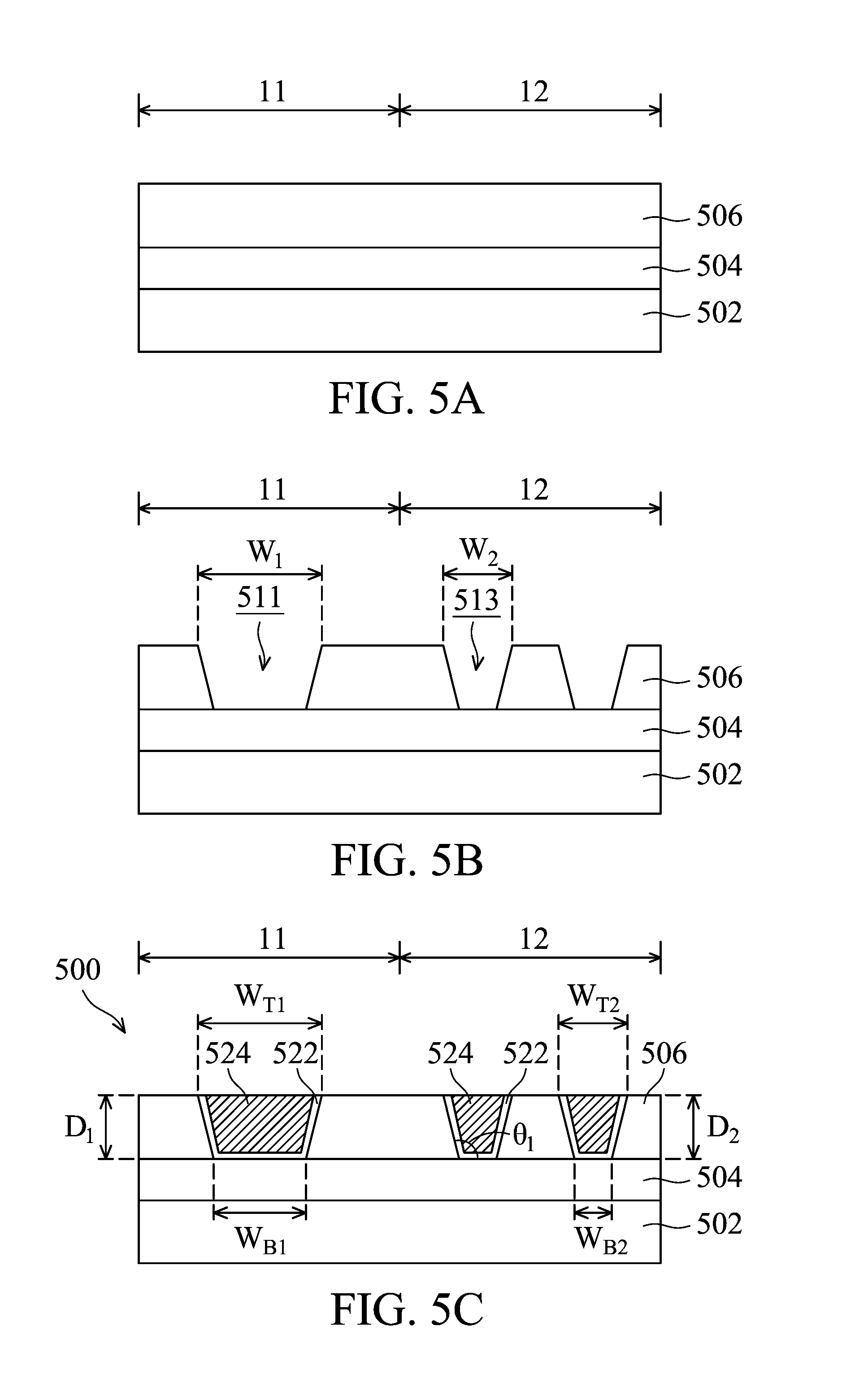
[0057] FIGS. 5A-5C show cross-sectional views of various stages of forming a semiconductor device structure 500, in accordance with some embodiments of the disclosure.
[0058] As shown in FIG. 5A, a substrate 502 is provided. An etching stop layer 504 is formed over the substrate 502. A material layer 506 is formed over the etching stop layer 504. The substrate 502 has a first region 11 and a second region 12.
[0059] Afterward, as shown in FIG. 5B, the material layer 506 is etched by performing an etching process on the material layer 506 to form a first trench 511 in the first region 11 and a second trench 513 in the second region, in accordance with some embodiments of the disclosure. The first trench 511 has a first top width W.sub.1, and the second trench 513 has a second top width W.sub.2. The first top width W.sub.1 is greater than the second top width W.sub.2.
[0060] For regions with different exposed areas (or etched areas), it is difficult to control etch uniformity due to the loading effect. Depending on the etching strategy, the loading effect is the etch rate for a high pattern density area being either faster or slower than it is for a low pattern density area. In other words, the loading effect is that the etch rate in a large area is mismatched to the etch rate in a small area. This means that the loading effect may be affected by pattern density.
[0061] In order to reduce the loading effect, by applying different first RF powers to the number of first sub-electrodes 112, the regions in the plasma chamber 102 may be controlled to have different plasma density. In some embodiments, the plasma density of the etching gas in the first region 11 is different from the plasma density of the etching gas in the second region 12. That is, although the pattern density in the first region 11 is different from that in the second region 12, the depth of the first trench 511 is substantially equal to the depth of the second trench 513 by separately controlling the first sub-electrodes 112 and the second sub-electrodes 122. In some embodiments, the density of the plasma is affected by the layout and the controller, and the etched depth and the critical dimension (CD) of the etched structure are determined by the density of the plasma. According to feedback of the etched depth, the critical dimension (CD) of the etched structure, the layout and the controller are controlled to obtain desirable etched profile.
[0062] Next, as shown in FIG. 5C, a diffusion barrier layer 522 is deposited in the first trench 511 and the second trench 513, and then a conductive layer 524 is formed on the diffusion barrier layer 522, in accordance with some embodiments of the disclosure. As a result, a first conductive structure 526 is constructed by the first diffusion barrier layer 522 and the conductive layer 524 in the first region 11. A second conductive structure 528 is constructed by the diffusion barrier layer 522 and the conductive layer 524 in the second region 12.
[0063] The first conductive structure 526 has a first depth D.sub.1 which is measured from a top surface of the conductive layer 524 to a bottom surface of the diffusion barrier layer 522. The second conductive structure 528 has a second depth D.sub.2 which is measured from a top surface of the conductive layer 524 to a bottom surface of the diffusion barrier layer 522. In some embodiments, a depth ratio (D.sub.1/D.sub.2) of the first depth D.sub.1 to the second depth D.sub.2 is in a range from about 0.8 to about 1.2.
[0064] In the first region 11, the first conductive structure 526 has a first top width W.sub.T1 and a first bottom width W.sub.B1. In some embodiments, a width ratio (W.sub.T1/W.sub.B1) of the first top width W.sub.T1 to the first bottom width W.sub.B1 is in a range from about 0.8 to about 1.2. In the second region 12, the second conductive structure 528 has a second top width W.sub.T2 and a second bottom width W.sub.B2. In some embodiments, a width ratio (W.sub.T/W.sub.B) of the second top width W.sub.T2 to the second bottom width W.sub.B2 is in a range from about 0.8 to about 1.2. A first angle .theta..sub.1 is between the bottom surface of the diffusion barrier layer 522 and a sidewall surface of the conductive layer 524. In some embodiments, the first angle .theta..sub.1 is in a range from about 70 degrees to about 90 degrees.
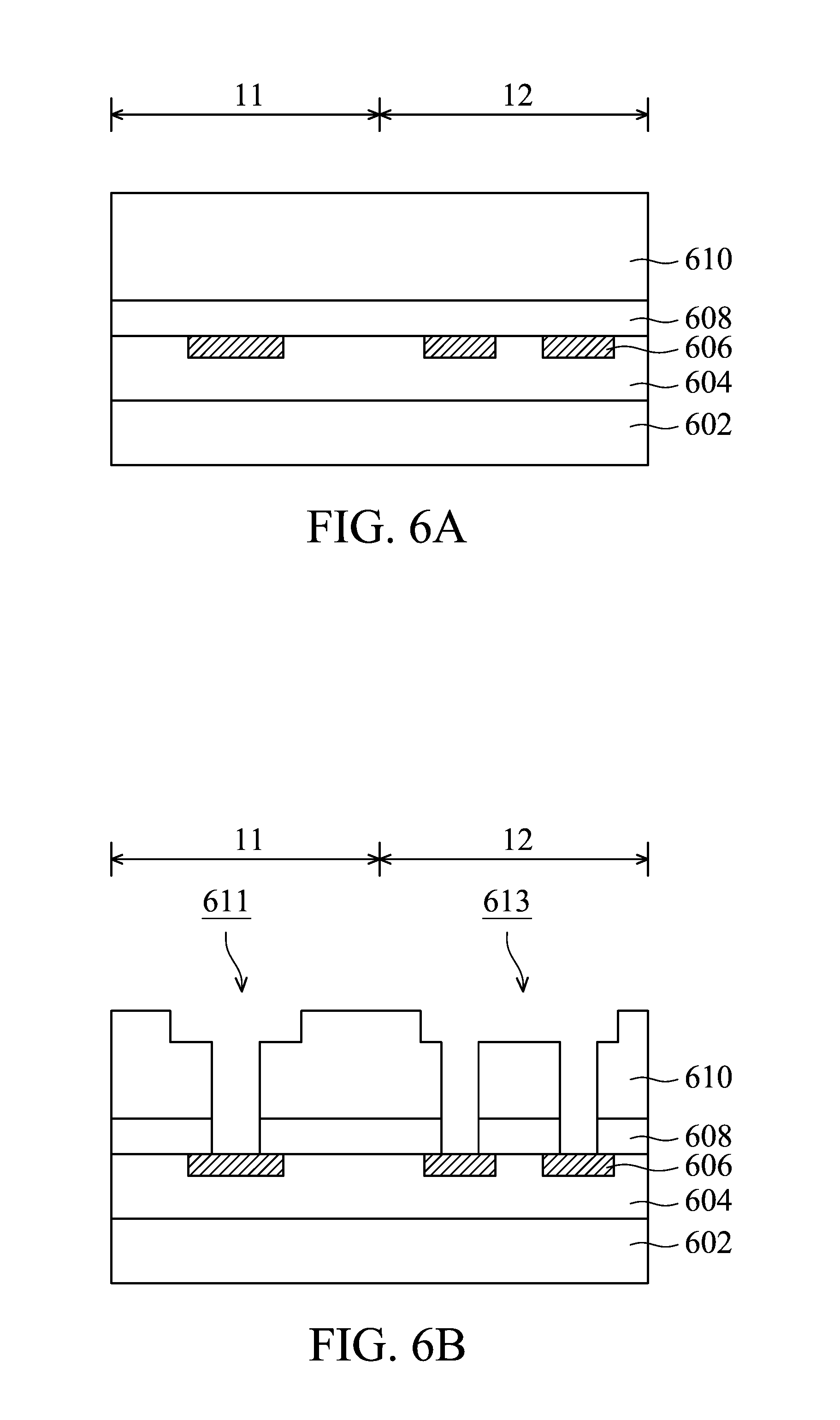
[0065] FIGS. 6A-6C show cross-sectional views of various stages of forming a semiconductor device structure 600, in accordance with some embodiments of the disclosure.
[0066] As shown in FIG. 6A, a first dielectric layer 604 is formed over a substrate 602, and a conductive layer 606 is formed in the first dielectric layer 604. An etching stop layer 608 is formed over the first dielectric layer 604, and a second dielectric layer 610 is formed over the etching stop layer 608.
[0067] Next, as shown in FIG. 6B, a first opening 611 is formed in the first region 11 and a second opening 613 is formed in the second region 12, in accordance with some embodiments of the disclosure. The first opening 611 is a first trench-via cavity for use as a dual damascene cavity. The second opening 613 is a second trench-via cavity for use as a dual damascene cavity.
[0068] The first opening 611 and the second opening 613 are formed by performing an etching process. The etching process is performed in the plasma processing apparatus 100 in FIG. 1. It should be noted that although the pattern density in the first region 11 is different from that in the second region 12, and the depth of the first opening 611 is substantially equal to the depth of the second opening 613 by using a number of first sub-electrodes 112 and a number of second sub-electrodes 122. The plasma density in the first region 11 and the second region 12 can be controlled by separately controlling each of the first sub-electrodes 112 and each of the second sub-electrodes 122 via the first matching units 114 and the second matching units 124.
[0069] Subsequently, as shown in FIG. 6C, a diffusion barrier layer 622 is deposited in the first opening 611 and the second opening 613, and then a conductive layer 624 is formed on the diffusion barrier layer 622, in accordance with some embodiments of the disclosure. As a result, a first trench-via structure 626 is formed in the first region 11 and a second trench-via structure 628 is formed in the second region 12. The first trench-via structure 626 is electrically connected to the conductive layer 606 in the first region 11, and the second trench-via structure 628 is electrically connected to the conductive layer 606 in the second region 12.
[0070] In the first region 11, the first trench-via structure 626 has a third top width W.sub.T3 and a third bottom width W.sub.B3. In some embodiments, a width ratio (W.sub.T3/W.sub.B3) of the third top width W.sub.T3 to the third bottom width W.sub.B3 is in a range from about 0.8 to about 1.2. In the second region 12, the second trench-via structure 628 has a fourth top width W.sub.T4 and a fourth bottom width W.sub.B4. In some embodiments, a width ratio (W.sub.T4/W.sub.B4) of the fourth top width W.sub.T4 to the fourth bottom width W.sub.B4 is in a range from about 0.8 to about 1.2. A second angle .theta..sub.2 is between the bottom surface of the diffusion barrier layer 622 and a sidewall surface of the conductive layer 624. In some embodiments, the second angle .theta..sub.2 is in a range from about 70 degrees to about 90 degrees.
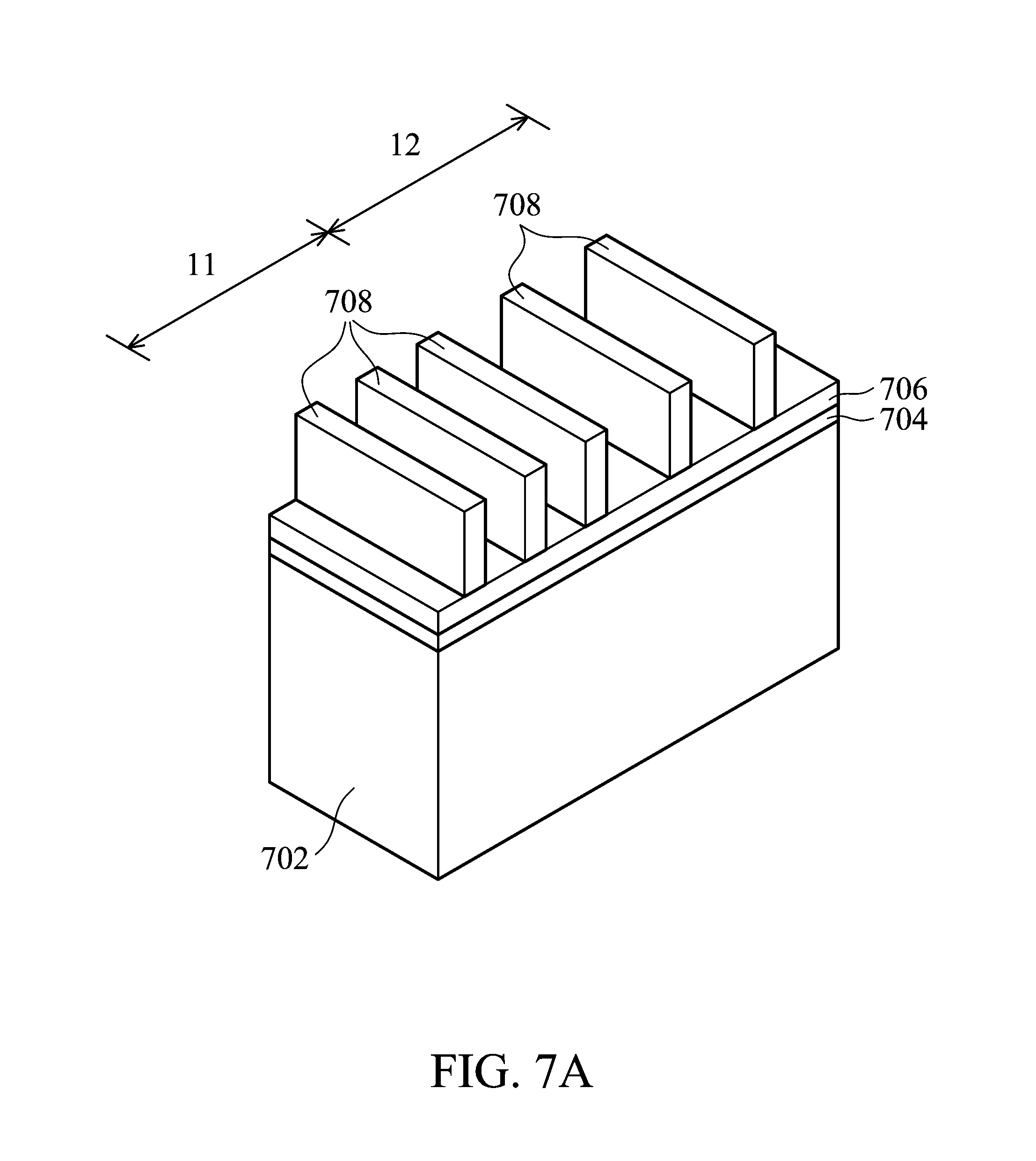
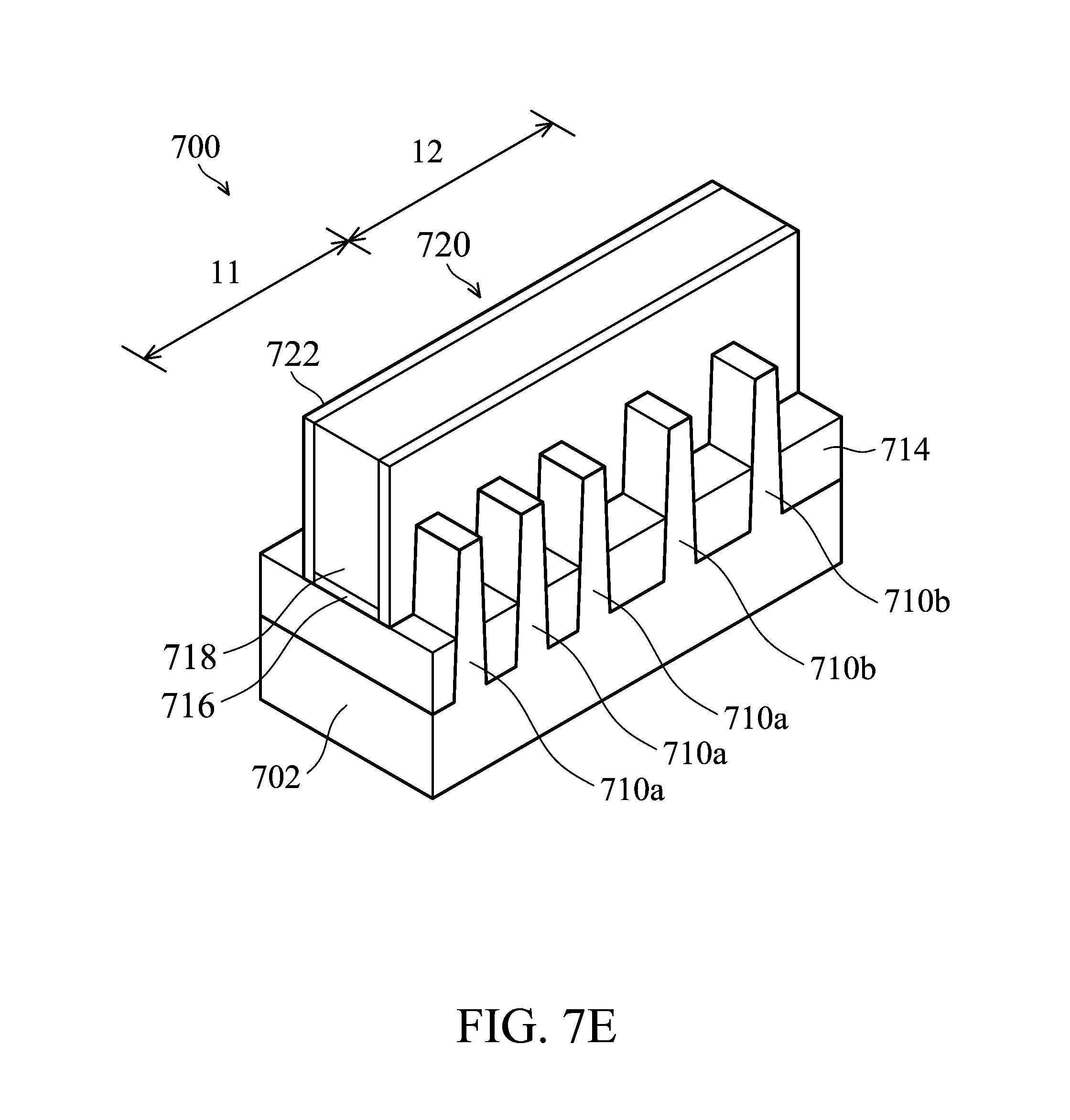
[0071] FIGS. 7A-7C show cross-sectional views of various stages of forming a semiconductor device structure 700, in accordance with some embodiments of the disclosure.
[0072] As shown in FIG. 7A, a substrate 702 is provided. The substrate 702 includes a first region 11 and a second region 12. Afterwards, a dielectric layer 704 and a mask layer 706 are formed over the substrate 702, and a photoresist layer 708 is formed over the mask layer 706. The photoresist layer 708 is patterned by a patterning process.
[0073] Next, as shown in FIG. 7B, after the photoresist layer 708 is patterned, the dielectric layer 704 and the mask layer 706 are patterned by using the patterned photoresist layer 708 as a mask, in accordance with some embodiments. As a result, a patterned dielectric layer 704 and a patterned mask layer 706 are obtained. Afterwards, the patterned photoresist layer 708 is removed.
[0074] Afterwards, an etching process is performed on the substrate 702 to form a number of fin structures 710a, 710b by using the patterned dielectric layer 704 and the patterned mask layer 706 as a mask. The fin structures 710a, 710b include first fin structures 710a in the first region 11 and second fin structures 710b in the second region 12. In some embodiments, each of the fin structures 710a, 710b has a width that gradually increases from the top portion to the bottom portion. In other words, each of the fin structures 710a, 710b has a tapered fin width which is gradually tapered from the bottom portion to the top portion. A first pitch P.sub.1 is between two adjacent fin structures 710a in the first region 11, and a second pitch P.sub.2 is between two adjacent fin structures 710b in the second region 12. The second pitch P.sub.2 is greater than the first pitch P.sub.1.
[0075] Each of the first fin structures 710a has a fifth top width W.sub.T5 and a fifth bottom width W.sub.B5. In some embodiments, a width ratio (W.sub.T5/W.sub.B5) of the fifth top width W.sub.T5 to the fifth bottom width W.sub.B5 is in a range from about 0.8 to about 1.2. A third angle .theta..sub.3 is between the bottom surface of the first fin structure 710a and a sidewall surface of the first fin structure 710a. In some embodiments, the third angle .theta..sub.3 is in a range from about 70 degrees to about 90 degrees.
[0076] Afterwards, as shown in FIG. 7C, after the fin structures 710a, 710b are formed, the isolation layer 712 is formed to cover the fin structures 710a, 710b over the substrate 702, in accordance with some embodiments.
[0077] Next, as shown in FIG. 7D, the isolation layer 712 is thinned or planarized to expose the top surface of the patterned mask layer 706. In some embodiments, the insulating layer 712 is thinned by a chemical mechanical polishing (CMP) process. Afterwards, a portion of the insulating layer 712 is removed to form an isolation structure 714, in accordance with some embodiments.
[0078] Afterwards, as shown in FIG. 7E, a gate dielectric layer 716 is formed on the fin structures 710a, 710b, the isolation structures 714a, 714b, and a gate electrode layer 718 is formed on the gate dielectric layer 716, in accordance with some embodiments. A gate structure 720 is constructed by the gate dielectric layer 716 and the gate electrode layer 718.
[0079] The disclosure provides a plasma processing apparatus. The first RF power source 116 is configured to provide different RF powers to the first sub-electrodes 112 to form a desired plasma density distribution in the plasma chamber 102. In addition, the second RF power source 126 is configured to provide different RF powers to the second sub-electrodes 122 to form a desired plasma density distribution in the plasma chamber 102.
[0080] The methods for forming the semiconductor device structures 500, 600,700 include using the plasma processing apparatus 100. In some embodiments, the substrate 502 with the material layer 506 (as shown in FIG. 5A) is positioned in the plasma chamber 102. A processing gas is supplied into the plasma chamber 102, and then the first RF power source 116 is applied to the first sub-electrodes 112 by the first matching units 114 to form a plasma. The material layer 506 is etched by using the plasma. In some other embodiments, in addition to applying the first RF power source 116 to the first sub-electrodes 112, the second RF power source 126 is simultaneously applied to the second sub-electrodes 122 by the second matching units 124.
[0081] The plasma density in the plasma chamber 102 can be controlled by adjusting the first height H.sub.1 of each of the first sub-electrodes 112. Furthermore, the cleaning process is performed in-situ after the etching process without transferring the substrate 170 to another chamber. Therefore, the risk of substrate pollution is reduced.
[0082] Embodiments for a plasma processing apparatus and method for formation a semiconductor device structure are provided. The plasma processing apparatus includes a plasma chamber including a housing, a first electrode array disposed outside the housing, and a number of first matching units outside the housing. The first electrode array includes a number of first sub-electrodes. The first sub-electrodes may be separately controlled by a number of first matching units. The plasma processing apparatus further includes a wafer support disposed in the plasma chamber. A second electrode array is disposed in the wafer support, and the second electrode array includes a number of second sub-second electrodes. The second sub-second electrodes may be separately controlled by a number of second matching units.
[0083] The first RF power source is configured to provide different RF powers to the first sub-electrodes to form a desired plasma density distribution in the different regions of the plasma chamber. The second RF power source is configured to provide different RF powers to the second sub-electrodes to form a desired plasma density distribution in the different regions of the plasma chamber. As a result, the etched depths or etched widths of the trench in different regions are controlled well by using the first sub-electrodes and the second sub-electrodes. Therefore, the quality and yield of the semiconductor device structure is improved.
[0084] In some embodiments, a plasma processing apparatus is provided. The plasma processing apparatus includes a plasma chamber including a housing, and a first electrode array disposed above and outside the housing. The first electrode array includes a plurality of first sub-electrodes. The plasma processing apparatus also includes a number of first matching units outside of the housing, and each of the first matching units is electrically connected to each of the first sub-electrodes.
[0085] In some embodiments, a plasma processing apparatus is provided. The plasma processing apparatus includes a plasma chamber including a housing and a wafer support. The plasma processing apparatus includes a top electrode array disposed above and outside the housing, and the top electrode array includes a plurality of top sub-electrodes. The top sub-electrodes are separate from each other. The plasma processing apparatus further includes a bottom electrode array disposed in the wafer support, and the bottom electrode includes a plurality of bottom sub-electrodes. The bottom sub-electrodes are separate from each other.
[0086] In some embodiments, a method for forming a semiconductor device structure is provided. The method includes placing a substrate with a material layer above the substrate in a plasma chamber. The plasma chamber includes a housing, a first electrode array disposed above and outside the housing, the first electrode array includes a plurality of first sub-electrodes, a number of first matching units electrically connected to each of the first sub-electrodes and a second electrode array disposed in the housing. The method includes supplying an etching plasma into the plasma chamber and applying a first RF power source to the first sub-electrodes of the first electrode array by each of the first matching units to form an etching plasma. The etching plasma has different plasma density in different regions above the substrate. The method includes performing an etching process on the material layer by the etching plasma.
[0087] The foregoing outlines features of several embodiments so that those skilled in the art may better understand the aspects of the present disclosure. Those skilled in the art should appreciate that they may readily use the present disclosure as a basis for designing or modifying other processes and structures for carrying out the same purposes and/or achieving the same advantages of the embodiments introduced herein. Those skilled in the art should also realize that such equivalent constructions do not depart from the spirit and scope of the present disclosure, and that they may make various changes, substitutions, and alterations herein without departing from the spirit and scope of the present disclosure.
* * * * *
D00000
D00001
D00002
D00003
D00004
D00005
D00006
D00007
D00008
D00009
D00010
D00011
D00012

D00013
D00014

D00015

D00016

D00017
XML
uspto.report is an independent third-party trademark research tool that is not affiliated, endorsed, or sponsored by the United States Patent and Trademark Office (USPTO) or any other governmental organization. The information provided by uspto.report is based on publicly available data at the time of writing and is intended for informational purposes only.
While we strive to provide accurate and up-to-date information, we do not guarantee the accuracy, completeness, reliability, or suitability of the information displayed on this site. The use of this site is at your own risk. Any reliance you place on such information is therefore strictly at your own risk.
All official trademark data, including owner information, should be verified by visiting the official USPTO website at www.uspto.gov. This site is not intended to replace professional legal advice and should not be used as a substitute for consulting with a legal professional who is knowledgeable about trademark law.