Method Of Selectively Depositing A Capping Layer Structure On A Semiconductor Device Structure
Kuroda; Aurelie ; et al.
U.S. patent application number 15/815483 was filed with the patent office on 2019-05-16 for method of selectively depositing a capping layer structure on a semiconductor device structure. The applicant listed for this patent is ASM IP Holding B.V.. Invention is credited to Dai Ishikawa, Akiko Kobayashi, Aurelie Kuroda.
| Application Number | 20190148224 15/815483 |
| Document ID | / |
| Family ID | 66433517 |
| Filed Date | 2019-05-16 |


| United States Patent Application | 20190148224 |
| Kind Code | A1 |
| Kuroda; Aurelie ; et al. | May 16, 2019 |
METHOD OF SELECTIVELY DEPOSITING A CAPPING LAYER STRUCTURE ON A SEMICONDUCTOR DEVICE STRUCTURE
Abstract
A method of selectively depositing a capping layer structure on a semiconductor device structure is disclosure. The method may include; providing a partially fabricated semiconductor device structure comprising a surface including a metallic interconnect material, a metallic barrier material, and a dielectric material. The method may also include; selectively depositing a first metallic capping layer over the metallic barrier material and over the metallic interconnect material relative to the dielectric material; and selectively depositing a second metallic capping layer over the first metallic capping layer relative to the dielectric material. Semiconductor device structures including a capping layer structure are also disclosed.
| Inventors: | Kuroda; Aurelie; (Tokyo, JP) ; Kobayashi; Akiko; (Tokyo, JP) ; Ishikawa; Dai; (Tokyo, JP) | ||||||||||
| Applicant: |
|
||||||||||
|---|---|---|---|---|---|---|---|---|---|---|---|
| Family ID: | 66433517 | ||||||||||
| Appl. No.: | 15/815483 | ||||||||||
| Filed: | November 16, 2017 |
| Current U.S. Class: | 438/653 |
| Current CPC Class: | H01L 21/76847 20130101; H01L 21/76849 20130101; H01L 21/7685 20130101; H01L 23/53238 20130101; H01L 21/76846 20130101; H01L 21/28562 20130101 |
| International Class: | H01L 21/768 20060101 H01L021/768; H01L 21/285 20060101 H01L021/285; H01L 23/532 20060101 H01L023/532 |
Claims
1. A method of selectively depositing a capping layer structure on a semiconductor device structure, the method comprising; providing a partially fabricated semiconductor device structure comprising a surface including a metallic interconnect material, a metallic barrier material, and a dielectric material; using a selective cyclical deposition process, selectively depositing a first metallic capping layer over the metallic barrier material and over the metallic interconnect material relative to the dielectric material; and using a selective chemical vapor deposition process, selectively depositing a second metallic capping layer over the first metallic capping layer relative to the dielectric material.
2. The method of claim 1, wherein the metallic barrier material comprises at least one of tantalum, tantalum nitride, titanium, titanium nitride, ruthenium, or manganese.
3. The method of claim 1, wherein selectively depositing a first metallic capping layer further comprises contacting the partially fabricated semiconductor device structure with a metal halide precursor.
4. The method of claim 3, wherein the metal halide precursor comprises at least one of a tungsten halide precursor, a titanium halide precursor, or a tantalum halide precursor.
5. The method of claim 1, wherein selectively depositing a first metallic capping layer comprises performing one or more sequential deposition cycles, each deposition cycle comprising alternating contacting the partially fabricated semiconductor device structure with a metal halide precursor and a reducing agent precursor.
6. The method of claim 5, wherein the metal halide precursor comprises at least one of tungsten hexafluoride (WF.sub.6), tungsten pentachloride (WCl.sub.5), titanium tetrachloride (TiCl.sub.4), or tantalum pentafluoride (TaF.sub.5).
7. The method of claim 5, wherein the reducing agent precursor comprises at least one of hydrogen (H.sub.2), a hydrogen (H.sub.2) plasma, ammonia (NH.sub.3), an ammonia (NH.sub.3) plasma, hydrazine (N.sub.2H.sub.4), silane (SiH.sub.4), disilane (Si.sub.2H.sub.6), trisilane (Si.sub.3H.sub.8), germane (GeH.sub.4), digermane (Ge.sub.2H.sub.6), or diborane (B.sub.2H.sub.6).
8. The method of claim 5, wherein the deposition cycle further comprises a purging cycle performed after contacting the partially fabricated semiconductor device structure with the metal halide.
9. The method of claim 5, wherein the deposition cycle further comprises a purging cycle performed after contacting the partially fabricated semiconductor device structure with the reducing agent precursor.
10. The method of claim 1, wherein the first metallic capping layer comprises at least one of tungsten, titanium, or tantalum.
11. The method of claim 1, wherein selectively depositing a first metallic capping layer comprises a selectivity greater than about 99%.
12. The method of claim 1, further comprising a purging cycle performed after selectively depositing the first metallic capping layer.
13. (canceled)
14. The method of claim 1, wherein the selective chemical vapor deposition process further comprises, simultaneously contacting the partially fabricated semiconductor device structure with at least a metal halide precursor and a reducing agent precursor.
15. The method of claim 14, wherein the metal halide precursor comprises at least one of tungsten hexafluoride (WF.sub.6), tungsten pentachloride (WCl.sub.5), titanium tetrachloride (TiCl.sub.4), or tantalum pentafluoride (TaF.sub.5).
16. The method of claim 14, wherein the reducing agent precursor comprises at least one of hydrogen (H.sub.2), a hydrogen (H.sub.2) plasma, ammonia (NH.sub.3), an ammonia (NH.sub.3) plasma, silane (SiH.sub.4), disilane (Si.sub.2H.sub.6), trisilane (Si.sub.3H.sub.8), germane (GeH.sub.4), digermane (Ge.sub.2H.sub.6), or diborane (B.sub.2H.sub.6).
17. The method of claim 1, wherein the selective chemical vapor deposition process has a selectivity greater than 90%.
18. The method of claim 1, wherein the second metallic capping layer comprises at least one of tungsten, tantalum, tantalum nitride, titanium, or titanium nitride.
19. The method of claim 1, further comprising selectively depositing the first metallic capping layer and selectively depositing the second metallic capping layer in the same reaction chamber.
20. The method of claim 1, further comprising selectively depositing the first metallic capping layer in a first reaction chamber and selectively depositing the second metallic capping in a second reaction chamber, wherein the first reaction chamber and the second reaction chamber are different reaction chambers of a cluster tool.
21. A method of selectively depositing a capping layer structure on a semiconductor device structure, the method comprising; providing a partially fabricated semiconductor device structure comprising a surface including a metallic interconnect material, a metallic barrier material, and a dielectric material, into a reaction chamber; contacting the partially fabricated semiconductor device structure with a first metal halide precursor, purging the reaction chamber; and simultaneously contacting the partially fabricated semiconductor device structure with a second metal halide precursor and a first reducing agent precursor.
22. The method of claim 21, wherein contacting the partially fabricated semiconductor device structure with a first metal halide precursor further comprises, contacting the partially fabricated semiconductor device structure with a second reducing agent precursor.
23. The method of claim 22, wherein contacting the partially fabricated semiconductor device structure with the first metal halide precursor and the second reducing agent precursor comprises one deposition and the method further comprises performing one or more deposition cycles.
24. The method of claim 21, further comprising performing a pre-treatment process on the partially fabricated semiconductor device structure prior to contacting the partially fabricated semiconductor device structure with the first metal halide, wherein the pre-treatment process is utilized to remove at least one of a passivation layer, a surface oxide, or a surface contaminant, from a surface of the metallic interconnect material.
25. A semiconductor device structure comprising a capping layer structure deposited by the method of claim 1.
Description
FIELD OF INVENTION
[0001] The present disclosure relates generally to methods for selectively depositing a capping layer structure on a semiconductor device structure and particularly methods for selectively depositing a metallic capping layer structure over a partially fabricated semiconductor device structure comprising a surface including a metallic interconnect material, a metallic barrier material, and a dielectric material.
BACKGROUND OF THE DISCLOSURE
[0002] Aluminum as a metallic interconnect material in integrated semiconductor circuits has essentially been replaced with alternative metallic interconnect materials primarily due to aluminums high electrical resistivity. One metallic interconnect material that is currently utilized is copper, due to copper's low electrical resistivity and durability. However, copper has certain disadvantages, particularly the capability of copper to diffuse into adjacent materials, such as adjacent, surrounding dielectric materials. Due to the diffusion ability of copper, a barrier material may be deposited over the dielectric material prior to copper deposition, the barrier material having properties enabling it to prevent copper diffusion. For example, the barrier material may comprise a metallic barrier material, such as, for example, tantalum based barrier materials and titanium based barrier materials. After the deposition of the copper interconnect the exposed copper line may require a capping layer, wherein the capping layer prevents oxidation of the copper interconnect and importantly prevents diffusion of the copper into an overlying dielectric material. In order to minimize the electrical resistivity of the interconnect, it is common to utilize metallic capping layers, such as, for example, tungsten (W), titanium (Ti), or tantalum (Ta).
[0003] In metallic interconnect applications it may be desirable to deposit a metallic capping layer selectively over the metallic interconnect. As a non-limiting example, it may be desirable to selectively deposit a tungsten capping layer over a copper interconnect, without depositing tungsten over the surrounding dielectric material. Typically, such discriminating results are achieved by depositing a continuous metallic film and subsequently patterning the metallic film using lithography and etch steps. Such lithography and etch processes may be time consuming and expensive, and do not offer the precision required in many interconnect applications. A possible solution is the use of selective deposition processes, whereby a metallic film is deposited only in the desired areas, thereby eliminating the need for subsequent patterning steps. Selective deposition processes for semiconductor device structure may take a number of forms, including, but not limited to, selective dielectric deposition on dielectric surfaces (DoD), selective dielectric deposition on metallic surfaces (DoM), selective metal deposition on dielectric surfaces (MoD), and selective metal deposition on metallic surfaces (MoM).
[0004] Selective metal deposition on metallic surfaces is of particular interest for interconnect applications as it may enable efficient selective deposition of a metallic capping layer structure over a metallic interconnect material. Accordingly, methods are desired for selectively depositing a metallic film on a metallic surface relative to a dielectric surface and particularly methods for selectively depositing a metallic capping layer structure over a metallic interconnect material.
SUMMARY OF THE DISCLOSURE
[0005] This summary is provided to introduce a selection of concepts in a simplified form. These concepts are described in further detail in the detailed description of example embodiments of the disclosure below. This summary is not intended to identify key features or essential features of the claimed subject matter, nor is it intended to be used to limit the scope of the claimed subject matter.
[0006] In some embodiments, a method for selectively depositing a capping layer structure on a semiconductor device structure is provided. The method may comprise: providing a partially fabricated semiconductor device structure comprising a surface including a metallic interconnect material, a metallic barrier material, and a dielectric material. The method may also comprise; selectively depositing a first metallic capping layer over the metallic barrier material and over the metallic interconnect material relative to the dielectric material; and selectively depositing a second metallic capping layer over the first metallic capping layer relative to the dielectric material.
[0007] In some embodiments, an additional method for selectively depositing a capping layer structure on a semiconductor device structure is provided. The method may comprise: providing a partially fabricated semiconductor device structure comprising a surface including a metallic interconnect material, a metallic barrier material, and a dielectric material, into a reaction chamber. The method may also comprise; contacting the partially fabricated semiconductor device structure with a first metal halide precursor, purging the reaction chamber, and simultaneously contacting the partially fabricated semiconductor device structure with a second metal halide precursor and a first reducing agent precursor.
[0008] For purposes of summarizing the invention and the advantages achieved over the prior art, certain objects and advantages of the invention have been described herein above. Of course, it is to be understood that not necessarily all such objects or advantages may be achieved in accordance with any particular embodiment of the invention. Thus, for example, those skilled in the art will recognize that the invention may be embodied or carried out in a manner that achieves or optimizes one advantage or group of advantages as taught or suggested herein without necessarily achieving other objects or advantages as may be taught or suggested herein.
[0009] All of these embodiments are intended to be within the scope of the invention herein disclosed. These and other embodiments will become readily apparent to those skilled in the art from the following detailed description of certain embodiments having reference to the attached figures, the invention not being limited to any particular embodiment(s) disclosed.
BRIEF DESCRIPTION OF THE DRAWING FIGURES
[0010] While the specification concludes with claims particularly pointing out and distinctly claiming what are regarded as embodiments of the invention, the advantages of embodiments of the disclosure may be more readily ascertained from the description of certain examples of the embodiments of the disclosure when read in conjunction with the accompanying drawings, in which:
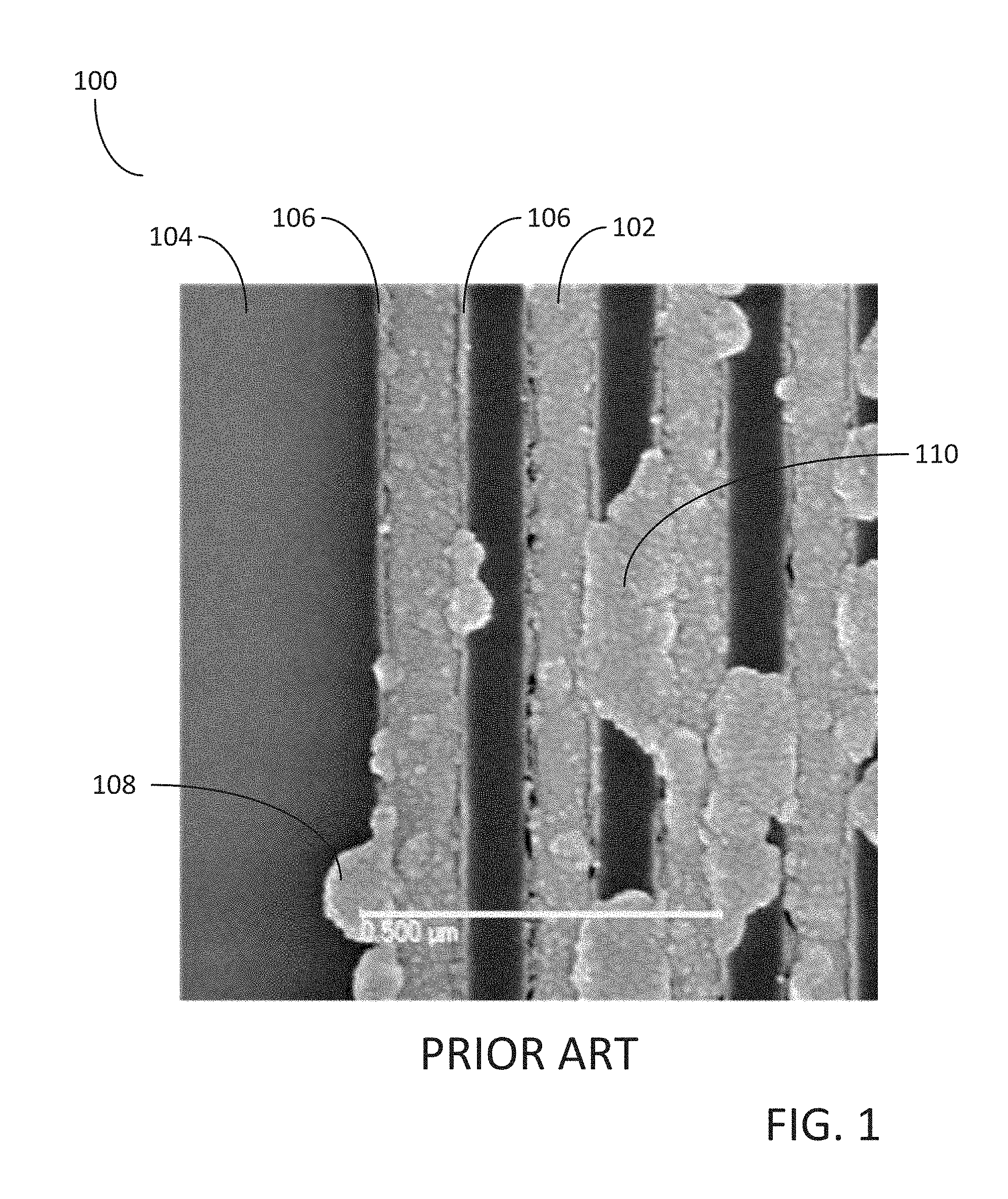
[0011] FIG. 1 illustrates a plan view scanning electron microscope image of a partially fabricated semiconductor device structure including a capping layer deposited utilizing prior art methods;
[0012] FIG. 2A illustrates a process flow diagram for an exemplary method of selectively depositing a metallic capping layer structure according to the embodiments of the disclosure;
[0013] FIG. 2B illustrates a portion of a process flow diagram for an exemplary method of selectively depositing a first metallic capping layer according to the embodiments of the disclosure;
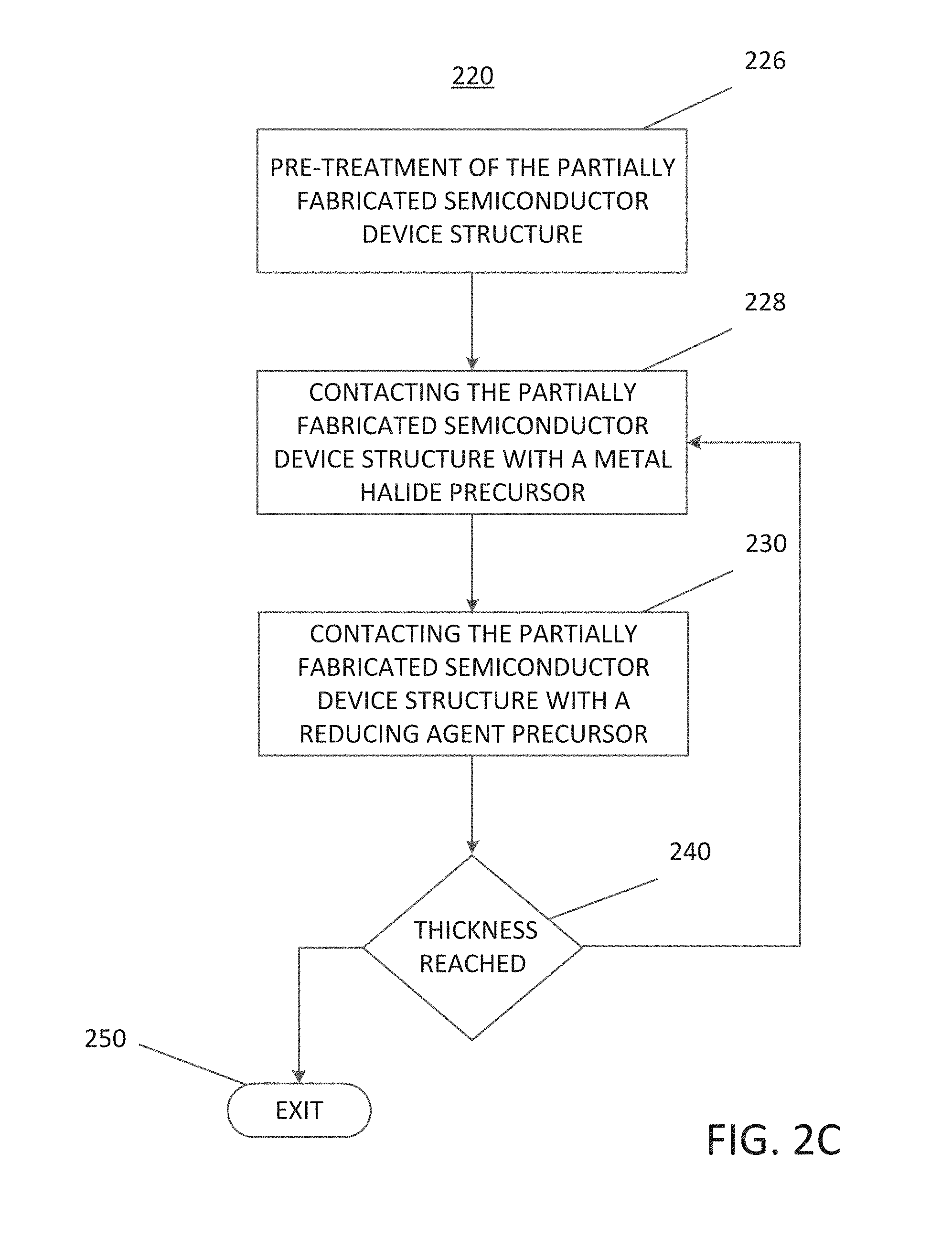
[0014] FIG. 2C illustrates a portion of a process flow diagram for an additional exemplary method of selectively depositing a first metallic capping layer according to the embodiments of the disclosure;
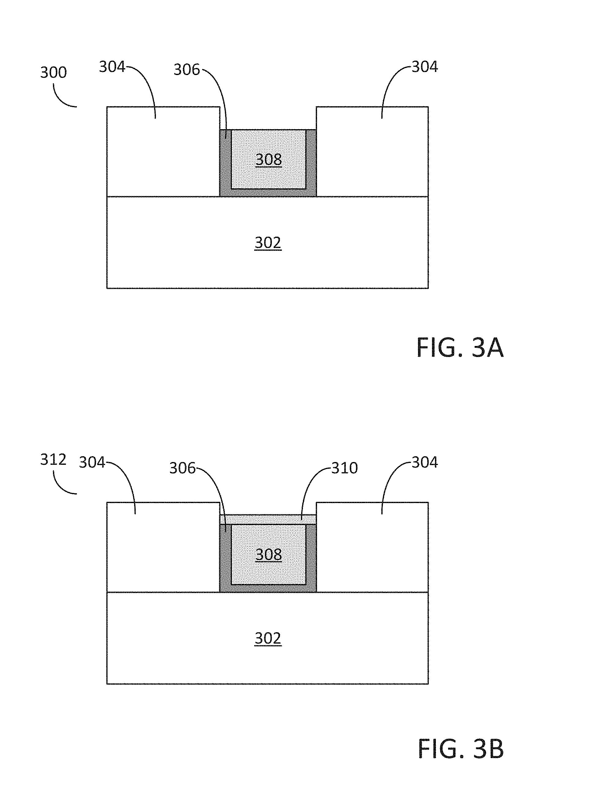
[0015] FIGS. 3A-C illustrate schematic cross section views of a process flow for selectively depositing a capping layer structure on a semiconductor device structure according to the embodiments of the disclosure;
[0016] FIG. 4A-B illustrate plan view scanning electron microscope images of partially fabricated semiconductor device structures including a metallic capping layer structure deposited according to the embodiments of the disclosure;
[0017] FIG. 5 illustrates a plan view scanning electron microscope image of an additional partially fabricated semiconductor device structure including a metallic capping layer structure deposited according to the embodiments of the disclosure.
DETAILED DESCRIPTION OF EXEMPLARY EMBODIMENTS
[0018] Although certain embodiments and examples are disclosed below, it will be understood by those in the art that the invention extends beyond the specifically disclosed embodiments and/or uses of the invention and obvious modifications and equivalents thereof. Thus, it is intended that the scope of the invention disclosed should not be limited by the particular disclosed embodiments described below.
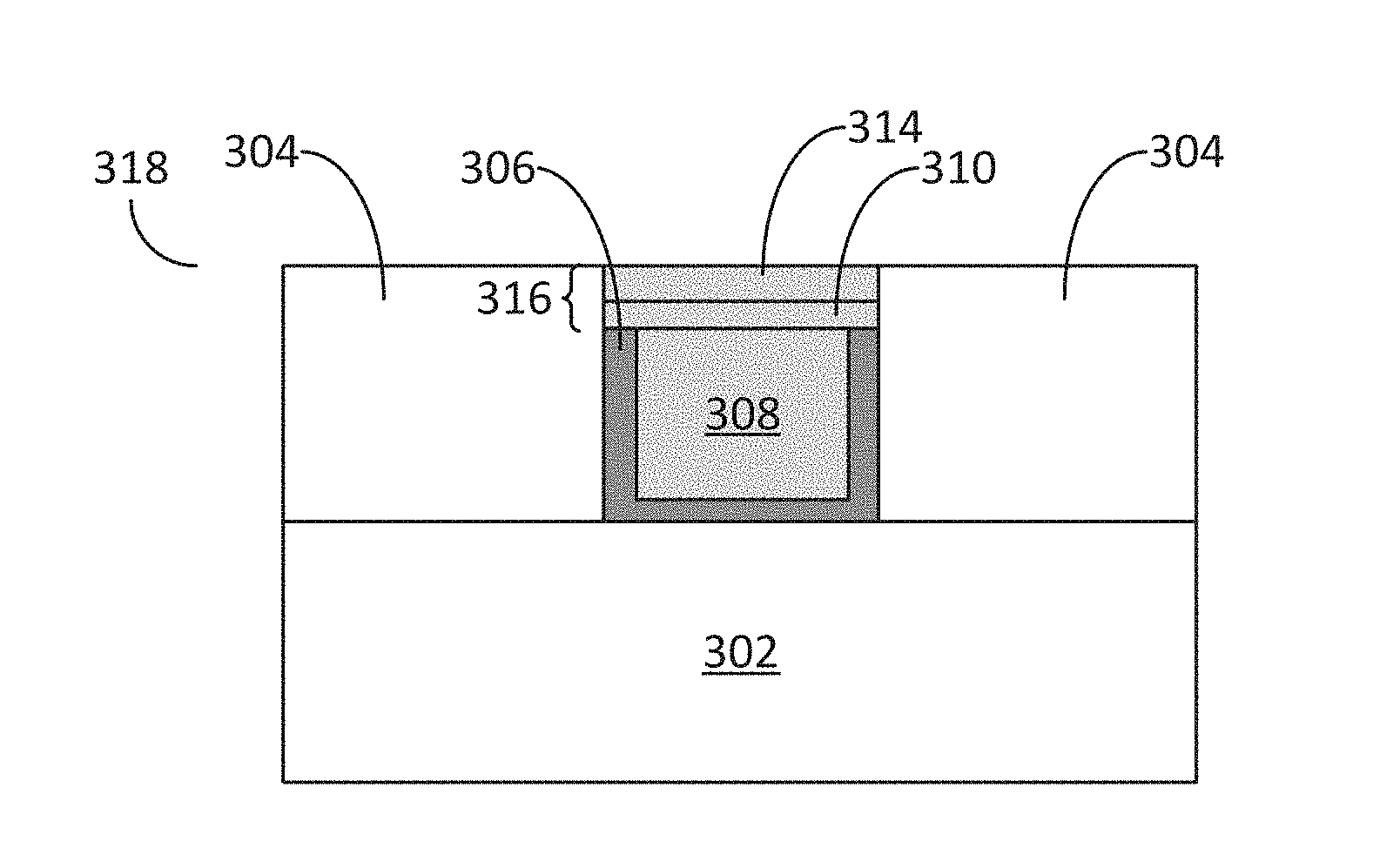
[0019] The illustrations presented herein are not meant to be actual views of any particular material, structure, or device, but are merely idealized representations that are used to describe embodiments of the disclosure.
[0020] As used herein, the term "semiconductor device structure" may refer to any portion of a processed semiconductor structure that is, includes, or defines at least a portion of an active or passive component of a semiconductor device to be formed on or in a semiconductor substrate. For example, semiconductor device structures may include, active and passive components of integrated circuits, such as, for example, transistors, memory elements, transducers, capacitors, resistors, conductive lines, conductive vias, and conductive contact pads.
[0021] As used herein, the terms "metallic interconnect material" and "metallic barrier materials" may refer to materials and surfaces including a metallic component, including, but not limited to, elemental metals, metal oxides, metal silicides, metal nitrides and metal carbides.
[0022] As used herein, the term "film" and "thin film" may refer to any continuous or non-continuous structures and materials deposited by the methods disclosed herein. For example, "film" and "thin-film" could include 2D materials, nanorods, nanotubes, or nanoparticles, or even partial or full molecular layers or partial or full atomic layers or clusters of atoms and/or molecules. "Film" and "thin-film" may comprise material or a layer with pinholes, but still be at least partially continuous.
[0023] As used herein, the term "chemical vapor deposition" may refer to any process wherein a substrate is exposed to one or more volatile precursors, which react and/or decompose on a substrate to produce a desired deposition.
[0024] As used herein, the term "cyclic deposition" may refer to the sequential introduction of precursors (reactants) into a reaction chamber to deposit a film over a substrate and includes deposition techniques such as atomic layer deposition and cyclical chemical vapor deposition.
[0025] As used herein, the term "cyclical chemical vapor deposition" may refer to any process wherein a substrate is sequentially exposed to two or more volatile precursors, which react and/or decompose on a substrate to produce a desired deposition.
[0026] As used herein, the term "substrate" may refer to any underlying material or materials that may be used, or upon which, a device, a circuit or a film may be formed.
[0027] As used herein, the term "atomic layer deposition" (ALD) may refer to a vapor deposition process in which deposition cycles, preferably a plurality of consecutive deposition cycles, are conducted in a process chamber. Typically, during each cycle the precursor is chemisorbed to a deposition surface (e.g., a substrate surface or a previously deposited underlying surface such as material from a previous ALD cycle), forming a monolayer or sub-monolayer that does not readily react with additional precursor (i.e., a self-limiting reaction). Thereafter, if necessary, a reactant (e.g., another precursor or reaction gas) may subsequently be introduced into the process chamber for use in converting the chemisorbed precursor to the desired material on the deposition surface. Typically, this reactant is capable of further reaction with the precursor. Further, purging steps may also be utilized during each cycle to remove excess precursor from the process chamber and/or remove excess reactant and/or reaction byproducts from the process chamber after conversion of the chemisorbed precursor. Further, the term "atomic layer deposition," as used herein, is also meant to include processes designated by related terms such as, "chemical vapor atomic layer deposition", "atomic layer epitaxy" (ALE), molecular beam epitaxy (MBE), gas source MBE, or organometallic MBE, and chemical beam epitaxy when performed with alternating pulses of precursor composition(s), reactive gas, and purge (e.g., inert carrier) gas.
[0028] A number of example materials are given throughout the embodiments of the current disclosure, it should be noted that the chemical formulas given for each of the example materials should not be construed as limiting and that the non-limiting example materials given should not be limited by a given example stoichiometry
[0029] The present disclosure includes methods that may be utilized to selectively deposit a capping layer structure over a metallic interconnect material and particular methods for selectively depositing a tungsten, titanium, or tantalum based capping layer structure over a metallic interconnect material surrounded by a metallic barrier material. The present disclosure also discloses methods for preventing selectivity loss originating due to unwanted interactions between the selective deposition precursors and a metallic barrier material.
[0030] In more detail, and as a non-limiting example of the methods of the disclosure, tungsten (W) may be selectively deposited over a metallic interconnect material, such as copper or cobalt, utilizing a selective chemical vapor deposition process. The selective chemical vapor deposition process may utilize tungsten hexafluoride (WF.sub.6) and hydrogen (H.sub.2) as the chemical precursors for the selective deposition of a tungsten film over a metallic material relative to a dielectric material. However, tungsten hexafluoride (WF.sub.6) may react with a metallic barrier material, such as, for example, titanium or tantalum, disposed adjacent to the metallic interconnect material. The reaction of the tungsten hexafluoride (WF.sub.6) with the metallic barrier material may produce metallic fluoride products that are volatiles, such as, for example, titanium fluorides and tantalum fluorides. The volatile metallic fluoride products may migrate into the adjacent dielectric surfaces. The hydrogen (H.sub.2) precursor present in the reaction chamber may reduce the metallic fluoride products to elemental metals, such as, for example, titanium and tantalum, which may be formed on the surface of the dielectric material, i.e., resulting in a loss of deposition selectivity between the metallic surfaces and the dielectric surfaces. The problem is further impacted as the unwanted elemental metal deposition on the dielectric material (e.g., titanium or tantalum) may act as a seed layer for the nucleation of tungsten (W) leading to a further increase in unwanted metal deposition on the dielectric material and a further loss of selectivity in the deposition process.
[0031] An example of such a loss in deposition selectivity between deposition on a metallic material relative to a dielectric material is illustrated in FIG. 1. FIG. 1 illustrates a plan-view scanning electron microscope image of a semiconductor structure 100 including a copper interconnect 102 embedded in a dielectric material 104. Disposed adjacent to and surrounding the copper interconnect is a barrier material 106 comprising tantalum. A selective chemical vapor deposition process was performed on the semiconductor structure to selectively deposit a tungsten capping layer over the copper interconnects. The selective chemical vapor deposition process utilized tungsten hexafluoride (WF.sub.6) and hydrogen (H.sub.2) as the precursor chemicals.
[0032] As evident in FIG. 1, the selective deposition process results in unwanted deposition on the dielectric material as indicated by example deposits 108 and 110, wherein unwanted deposit 110 results in a metal bridge between two copper lines leading to an electrical short. Accordingly methods are desirable for the selective deposition of a metallic capping layer structure on a metallic interconnect material relative to a dielectric material which maintains selectivity throughout the deposition process.
[0033] A selective deposition process may involve depositing a greater amount of material over a first material relative to a second material. In some embodiments of the disclosure, an exposed surface may comprise three materials and the selective deposition process may involve depositing a greater amount of material over a first material and over a second material relative to a third material. As used herein, the term "relative to" may refer to a comparison of the amount of material deposited on a first surface (and an optional second surface) compared to the amount of material deposited on a third surface, i.e., the thickness of material deposited on the first surface (and optional second surface) compared to the thickness of material deposited on the third surface. For example, for a metal on metal selective deposition process, the selective deposition process may deposit a greater amount of a metallic film on a first metallic surface relative to a second dielectric surface. In some embodiments of the disclosure, the selectivity of the deposition process may be expressed as the ratio of material deposited on the first surface relative to the amount of material formed on the first and second surfaces combined. For example, if a selective deposition process deposits 10 nm of tungsten on a first metallic surface and 1 nm of tungsten on a second dielectric surface, the selective deposition process will be considered to have 90% selectivity. In some embodiments, the selectivity of the methods disclosed herein may be above about 80%, above about 90%, above about 95%, or even about 100%. In some embodiments, the selectivity of the deposition process is at least about 80%, which may be selective enough for some particular applications. In some cases the selectivity is at least about 50%, which may be selective enough for some particular applications. In some embodiments of the disclosure, the selective deposition processes disclosed herein are achieved without the use of an etchant, such as, for example, an etchant gas.
[0034] In some embodiments of the disclosure, methods are disclosed which may comprise: providing a partially fabricated semiconductor device structure comprising a surface including a metallic interconnect, a metallic barrier material, and a dielectric material. The methods of the disclosure may also include; selectively depositing a first metallic capping layer over the metallic barrier material and over the metallic interconnect material relative to the dielectric material; and selectively depositing a second metallic capping layer over the first metallic capping layer relative to the dielectric material.
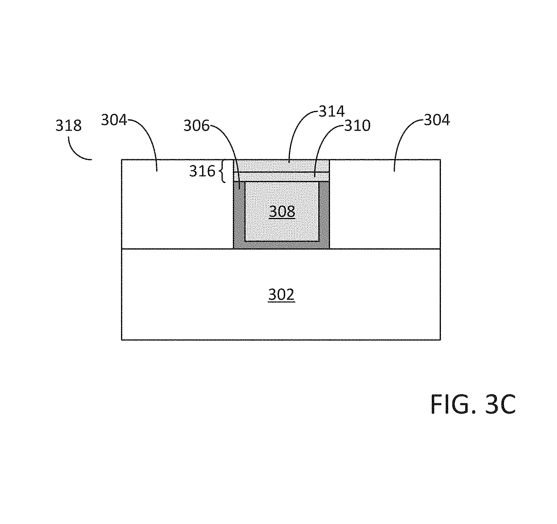
[0035] The methods of the disclosure are described in greater detail with reference to FIGS. 2A-C and FIGS. 3A-C. FIG. 2A illustrates an exemplary overall process flow for the selective deposition of a metallic capping layer structure. FIG. 2B illustrates a portion of the overall process flow and particularly illustrates a method for selectively depositing the first metallic capping layer by exposing a partially fabricated semiconductor device structure to a metal halide precursor. FIG. 2C illustrates a portion of the overall process flow and particularly illustrates an alternative method for selectively depositing the first metallic capping layer by performing a selective cyclical deposition process. FIG. 3A-C illustrate cross sectional schematic diagrams of the process flow of an exemplary selective deposition method according to the embodiments of the disclosure.
[0036] In more detail and with reference to FIG. 2A, an exemplary method 200 may begin with a process block 210 which comprises, providing a partially fabricated semiconductor device structure comprising a surface including a metallic interconnect material, a metallic barrier material, and a dielectric material. The partially fabricated semiconductor device structure 300 is illustrated in FIG. 3A and comprises a substrate 302, a dielectric material 304, a metallic barrier material 306, and a metallic interconnect material 308.
[0037] In some embodiments of the disclosure, the substrate 302 may comprise one or more materials including, but not limited to, silicon, silicon germanium (Si.sub.1-xGe.sub.x), silicon germanium tin (Si.sub.xGe.sub.1-xSn.sub.y), germanium, silicon carbide, and III-V semiconductors. Although not illustrated in FIG. 3A, the substrate 302 may include one or more semiconductor device structures formed into or onto a surface of the substrate 302. For example, the substrate may comprise partially fabricated and/or fabricated semiconductor device structures such as transistors and memory elements.
[0038] In some embodiments of the disclosure, the partially fabricated semiconductor device structure 300 may also include a dielectric material 304 formed over the substrate 302. In some embodiments, the dielectric material 304 may comprise a low dielectric constant material, i.e., a low-k material, which may be defined as a dielectric material having a dielectric constant less than about 4.0. In some embodiments, the dielectric constant of the low-k material may be less than 3.5, or less than 3.0, or less than 2.5, or even less than 2.3. In some embodiments, the dielectric material 304 may comprise a silicon containing dielectric material, including, but not limited to, a silicon oxide, a silicon nitride, a silicon oxynitride, or mixtures thereof. In some embodiments, the dielectric material 304 may comprise a metal oxide material, including, but not limited to, a titanium oxide, a tantalum oxide, or an aluminum oxide.
[0039] In some embodiments of the disclosure, the partially fabricated semiconductor device structure 300 may also include a metallic barrier material 306 which prevents, or substantially prevents, the diffusion of the metallic interconnect material 308 into the surrounding dielectric material 304. In some embodiments, the metallic barrier material 306 may comprise an elemental metal, or a metal nitride. In some embodiments, the metallic barrier material 306 may comprise at least one of tantalum, tantalum nitride, titanium, titanium nitride, ruthenium, or manganese.
[0040] In some embodiments of the disclosure, the partially fabricated semiconductor device structure 300 may also include a metallic interconnect material 308 which may be utilized to electrically connect semiconductor device structures formed in and/or on substrate 302. In some embodiments the metallic interconnect material 308 may comprise at least one of copper (Cu), or cobalt (Co).
[0041] As illustrated in FIG. 3A, the upper exposed surface of the partially fabricated semiconductor device structure 300 may comprise a metallic barrier 306, a metallic interconnect material 308, and a dielectric material 304. In some embodiments and as illustrated in FIG. 3A the upper exposed surfaces of the metallic barrier material 306 and the metallic interconnect material 308 may be recessed relative to the upper exposed surface of the dielectric material 304. In alternative embodiments, the upper exposed surfaces of the metallic barrier material 306, the metallic interconnect material 308 and the dielectric material 304 may be substantially planar.
[0042] In some embodiments of the disclosure, the exemplary selective deposition process 200 may continue with a process block 220 which comprising, selectively depositing a first metallic capping layer and particularly selectively depositing a first metallic capping layer over the metallic barrier material and over the metallic interconnect material relative to the dielectric material, in other words, the first metallic capping layer is deposited over the metallic barrier material and over the metallic interconnect material whereas no deposition, or substantially no deposition, occurs over the dielectric material.
[0043] In more detail and with reference to FIG. 3B, a first metallic capping layer 310 may be selectively deposited over the partially fabricated semiconductor device structure 300 such that the first metallic capping layer 310 may be disposed over the metallic barrier material 306 and over the metallic interconnect material 308. In some embodiments, the first metallic capping layer 310 may be disposed directly over the metallic barrier material 306 and directly over the metallic interconnect material 308. In contrast, and as illustrated in FIG. 3B, the selective deposition process for depositing the first metallic capping layer 300 deposits no metallic material, or substantially no metallic material, over the dielectric material 304, i.e., the surface of the dielectric material 304 is free of, or substantially free of, a deposited first metallic capping layer.
[0044] In some embodiments of the disclosure the process block 220, which comprises selectively depositing a first metallic capping layer, may be described in greater detail with reference to FIG. 2B which illustrates a process flow for selectively depositing the first metallic capping layer. The process block 220 may comprise a sub-process block 222 which comprises performing a pre-treatment process on the partially fabricated semiconductor device structure 300. In some embodiments, the pretreatment process may be utilized to remove any surface passivation layers, contaminants and/or surface oxides from the exposed surface of the metallic interconnect material 308. In some embodiments, the metallic interconnect material 308 may comprise copper and the surface of the copper interconnect may be at least partially covered with one or more of a passivation layer, contaminants, and/or a surface oxide. For example, the passivation layer may comprise benzotriazole (BTA), or a benzotriazole derivative, and the surface oxide may comprise a copper oxide.
[0045] The sub-process block 222 which comprises, performing a pre-treatment process on the partially fabricated semiconductor device, may proceed by loading the partially fabricated semiconductor device structure into a reaction chamber, i.e., into a pre-treatment reaction chamber. In some embodiments, the partially fabricated semiconductor device structure 300 may be heated to a pre-treatment process temperature of less than 500.degree. C., or less than 400.degree. C., or less than 300.degree. C., or even less than 200.degree. C. In some embodiments, the partially fabricated semiconductor device structure 300 is heated to a pre-treatment process temperature of approximately 300.degree. C.
[0046] The pressure within the pre-treatment reaction chamber may be also regulated. For example, the pressure within the pre-treatment reaction chamber may be approximately 300 Pascals.
[0047] In some embodiments of the disclosure, the pre-treatment process may further comprise, contacting the surface of the metallic interconnect material with an etchant gas comprising formic acid (HCOOH) and hydrogen (H.sub.2). For example, the formic acid (HCOOH) maybe introduced into the pre-treatment reaction chamber at a flow rate of 0.1 slm and the hydrogen may introduced into the pre-treatment reaction chamber at a flow rate of 0.5 slm. The annealing of the partially fabricated semiconductor device structure 300 in formic acid and hydrogen may be performed for a time period of less than 10 minute, or less than 5 minutes, or less than 3 minutes. In some embodiments, the partially fabricated semiconductor device structure 300 may be annealed at a temperature of 300.degree. C. in an atmosphere of formic acid and hydrogen for a time period of 5 minutes. Upon completion of the pre-treatment process, the surface of the metallic interconnect 300 may be free of passivating layers, contaminants, and/or metal oxides. In addition, upon completion of the pre-treatment process, the partially fabricated semiconductor device structure may be allowed to cool in a hydrogen atmosphere. For example, the partially fabricated semiconductor device structure may be allowed to cool to room temperature whilst introducing hydrogen into the pre-treatment reaction chamber at a flow rate of 0.5 slm.
[0048] The process for selectively depositing the first metallic capping layer may proceed with a sub-process block 224 (FIG. 2B), which comprises, contacting the partially fabricated semiconductor device structure with a metal halide precursor. In more detail, the partially fabricated semiconductor device structure may be transferred from a pre-treatment reaction chamber to a first deposition chamber. In some embodiments, the transfer of the partially fabricated semiconductor device structure from the pre-treatment chamber to the first deposition chamber may be performed under a controlled atmosphere such that the partially fabricated semiconductor device structure 300 is not exposed to external ambient conditions which could result in the oxidation of the exposed surface of the metallic interconnect material 308.
[0049] Upon transfer of the partially fabricated semiconductor device structure 300 to the first deposition chamber, the partially fabricated semiconductor device structure 300 may be heated to a desired deposition temperature. In some embodiments of the disclosure, the selective deposition of the first metallic capping layer may comprise, heating the partially fabricated semiconductor device structure to a temperature of less than 500.degree. C., or less than 400.degree. C., or even less than 300.degree. C. In some embodiments, the selective deposition of the first metallic capping layer may comprise heating the partially fabricated semiconductor device structure 300 to a deposition temperature of approximately 340.degree. C.
[0050] Once the partially fabricated semiconductor device structure 300 is heated to a desired deposition temperature, the partially fabricated semiconductor device structure 300 may be exposed to the metal halide precursor. In some embodiments, the metal halide precursor may comprise at least one of a tungsten halide precursor, a titanium halide precursor, or a tantalum halide precursor. In some embodiments, the metal halide precursor may comprise a tungsten halide precursor, such as, for example, tungsten hexafluoride (WF.sub.6), or tungsten pentachloride (WCl.sub.5). In some embodiments, the metal halide precursor may comprise a titanium halide precursor, such as, for example, titanium tetrachloride (TiCl.sub.4). In some embodiments, the metal halide precursor may comprise a tantalum precursor, such as, for example, tantalum pentafluoride (TaF.sub.5).
[0051] In some embodiments, the partially fabricated semiconductor device structure 300 may be contacted with the metal halide precursor for a time period greater than 30 seconds, or great than 1 minute, or greater than 3 minutes, or even greater than 5 minutes. In some embodiments, an additional inert gas may be introduced into the first deposition chamber simultaneously with the metal halide precursor, for example, the inert gas may comprise argon (Ar). In some embodiments, the flow rate of the metal halide precursor into the first deposition chamber may be approximately 20 sccm.
[0052] In some embodiments of the disclosure, contacting the partially fabricated semiconductor device structure 300 with the metal halide precursor results in the selective deposition of the first metallic capping layer 310 over the metallic barrier material 306 and over the metallic interconnect material 308, without depositing any, or significantly, any metallic material over the dielectric material 304 (FIG. 3B). In some embodiments, the first metallic capping layer 300 may be deposited to a thickness of less than 30 Angstroms, or less than 20 Angstroms, or even less than 10 Angstroms. In some embodiments of the disclosure, the first metallic capping layer 310 may be deposited to a thickness such that at least the upper exposed surface of the metallic barrier material 306 is substantially covered, or completely covered, with the first metallic capping layer 310. Not to be bound any theory, but it is believe that the sealing of the upper exposed surface of the metallic barrier material 306 substantially, or completely, prevents loss of deposition selectivity in subsequent selective deposition processes.
[0053] In additional embodiments of the disclosure the process block 220 (FIG. 2A), which comprises selectively depositing a first metallic capping layer, may be described in greater detail with reference to FIG. 2C which illustrates an alternative process flow for selectively depositing the first metallic capping layer.
[0054] With continued reference to FIG. 2C, the process block 220 may comprise a sub-process block 226 which comprises performing a pre-treatment process on the partially fabricated semiconductor device structure 300. The pre-treatment process 226 may be identical that previous described for the sub-process block 222 of FIG. 2B and therefore the pre-treatment process details are not repeated here. Upon completion of the pre-treatment process, the partially fabricated semiconductor device structure may be transferred to a first deposition chamber under controlled atmospheric conditions, as previous described.
[0055] Upon transferring the partially fabricated semiconductor device structure to the first deposition chamber, the method may continue by selectively depositing the first metallic capping layer over the metallic interconnect material 308 and over the metallic barrier material 306 relative to the dielectric material 304. In some embodiments of the disclosure, the method of selectively depositing the first metallic capping layer may comprise a selective cyclical deposition process, such as, for example, a selective atomic layer deposition process or a selective cyclical chemical vapor deposition process.
[0056] A non-limiting example embodiment of a selective cyclical deposition process may include selective atomic layer deposition (ALD), wherein ALD is based on typically self-limiting reactions, whereby sequential and alternating pulses of reactants are used to deposit about one atomic (or molecular) monolayer of material per deposition cycle. The deposition conditions and precursors are typically selected to provide self-saturating reactions, such that an adsorbed layer of one reactant leaves a surface termination that is non-reactive with the gas phase reactants of the same reactant. The substrate is subsequently contacted with a different reactant that reacts with the previous termination to enable continued deposition. Thus, each cycle of alternated pulses typically leaves no more than about one monolayer of the desired material. However, as mentioned above, the skilled artisan will recognize that in one or more ALD cycles more than one monolayer of material may be deposited, for example, if some gas phase reactions occur despite the alternating nature of the process.
[0057] In an selective ALD-type process for selectively depositing a first metallic capping layer and particularly selectively depositing a tungsten, titanium, or tantalum first metallic capping layer, one deposition cycle may comprise exposing the partially fabricated semiconductor device structure to a first reactant, removing any unwanted unreacted first reactant and reaction byproducts from the reaction space, and exposing the partially fabricated semiconductor device structure to a second reactant, followed by a second removal step. The first reactant may comprise a metal precursor and the second reactant may comprise a reducing agent precursor.
[0058] Precursors may be separated by inert gases, such as argon (Ar) or nitrogen (N.sub.2), to prevent gas-phase reactions between the reactants and enable self-saturating surface reactions. In some embodiments, however, the substrate may be moved to separately contact a first vapor phase reactant and a second vapor phase reactant. Because the reactions self-saturate, strict temperature control of the substrates and precise dosage control of the precursors may not be required. However, the substrate temperature is preferably such that an incident gas species does not condense into monolayers nor decompose on the surface. Surplus chemicals and reaction byproducts, if any, are removed from the substrate surface, such as, for example, by purging the reaction space or by moving the substrate, before the substrate is contacted with the next reactive chemical. Undesired gaseous molecules can be effectively expelled from a reaction space with the help of an inert purging gas. A vacuum pump may be utilized to assist in the purging process.
[0059] In some embodiments of the disclosure, the selective cyclical deposition processes are used to selectively deposit the first metallic capping layer on a partially fabricated semiconductor device structure and the selective cyclical deposition process may be a selective ALD type process. In some embodiments, the selective cyclical deposition may be a hybrid ALD/CVD or cyclical CVD process. For example, in some embodiments the growth rate of the ALD process may be low compared with a CVD process. One approach to increase the growth rate may be that of operating at a higher temperature than that typically employed in an ALD process, resulting in a chemical vapor deposition process, but still taking advantage of the sequential introduction of precursors, such a process may be referred to as cyclical CVD.
[0060] According to some embodiments of the disclosure, a selective ALD process may be utilized to selectively deposit a first metallic capping layer over a metallic barrier material and over a metallic interconnect material relative to a dielectric material. In some embodiments of the disclosure, each ALD cycle comprises two distinct deposition steps or phases. In a first phase of the deposition cycle ("the metal phase"), the partially fabricated semiconductor device structure surface on which deposition is desired is contacted with a first vapor phase reactant comprising a metal precursor, which chemisorbs on the surface of the partially fabricated semiconductor device structure, forming no more than about one monolayer of reactant species on the surface. In a second phase of the deposition cycle ("the reducing phase"), the partially fabricated semiconductor device structure is contacted with a second vapor phase reactant comprising a reducing agent precursor, wherein the reducing agent precursor may react with metal containing species on the surface of the partially fabricated semiconductor device structure to selectively deposit a first metallic capping layer.
[0061] In more detail, the process for selectively depositing the first metallic capping layer may comprise sub-process 228 (FIG. 2C) which includes contacting the partially fabricated semiconductor device structure with a metal halide precursor. In some embodiments, the metal halide precursor may comprise at least one of a tungsten halide precursor, a titanium halide precursor, or a tantalum halide precursor. In some embodiments, the metal halide precursor may comprise a tungsten halide precursor, such as, for example, tungsten hexafluoride (WF.sub.6), or tungsten pentachloride (WCl.sub.5). In some embodiments, the metal halide precursor may comprise a titanium halide precursor, such as, for example, titanium tetrachloride (TiCl.sub.4). In some embodiments, the metal halide precursor may comprise a tantalum precursor, such as, for example, tantalum pentafluoride (TaF.sub.5).
[0062] In some embodiments of the disclosure, contacting the partially fabricated semiconductor device structure with a metal halide precursor may comprise exposing the partially fabricated semiconductor device structure to the metal halide precursor for a time period of between about 0.01 seconds and about 50 seconds, between about 0.5 seconds and about 10 seconds, or between about 0.1 seconds and about 5 seconds. In some embodiments, the partially fabricated semiconductor device structure may be exposed to the metal halide precursor for a time period of 0.2 seconds. In addition, during the pulsing of the metal halide precursor over the partially fabricated semiconductor device structure, the flow rate of the metal halide precursor may be less than 2000 sccm, or less than 500 sccm, or even less than 100 sccm. In some embodiments, the flow rate of the metal halide into the reaction space and over the partially fabricated semiconductor device structure may be approximately 20 sccm. In some embodiments, an additional inert gas may be co-flowed with the metal halide precursor to maintain a constant flow-rate of gas species into the reaction space during the selective cyclical deposition process. For example, the additional inert gas may comprise argon (Ar) and may be introduced into the reaction space and over the partially fabricated semiconductor device structure at a flow rate of approximately 0.3 slm.
[0063] Excess metal halide precursor and reaction byproducts (if any) may be removed from the surface of the partially fabricated semiconductor device structure, e.g., by pumping with an inert gas. For example, in some embodiments of the disclosure, the methods may comprise a purge cycle wherein the partially fabricated semiconductor device structure surface is purged for a time period of less than 10 seconds, or less than 5 seconds, or less than 1 second. In some embodiments, the purge cycle may be performed for a time period of approximately 4 seconds. Excess metal halide precursor and any reaction byproducts may be removed with the aid of a vacuum, generated by a pumping system, in fluid communication with the reaction chamber.
[0064] The process for selectively depositing the first metallic capping layer may further comprise sub-process 230 (FIG. 2C) which includes contacting the partially fabricated semiconductor device structure with a reducing agent precursor. For example, in a second phase of the deposition cycle ("the reducing phase") the partially fabricated semiconductor device structure may be contacted with a second vapor phase reactant which may comprise a reducing agent precursor. In some embodiments, the reducing agent precursor may comprise at least one of hydrogen (H.sub.2), a hydrogen (H.sub.2) plasma, ammonia (NH.sub.3), an ammonia (NH.sub.3) plasma, hydrazine (N.sub.2H.sub.4), silane (SiH.sub.4), disilane (Si.sub.2H.sub.6), trisilane (Si.sub.3H.sub.8), germane (GeH.sub.4), digermane (Ge.sub.2H.sub.6), or diborane (B.sub.2H.sub.6). In particular embodiments of the disclosure, the reducing agent precursor may comprise hydrogen (H.sub.2), or a hydrogen (H.sub.2) plasma.
[0065] In some embodiments, contacting the partially fabricated semiconductor device structure with a reducing agent precursor may comprise pulsing the reducing agent precursor over the partially fabricated semiconductor device structure for a time period of between about 0.1 seconds and about 2.0 seconds, or from about 0.01 seconds to about 10 seconds, or less than about 20 seconds, or less than about 10 seconds, or less than about 5 seconds. In some embodiments, the partially fabricated semiconductor device structure may be contacted with the reducing agent precursor for a time period of approximately 5 seconds. During the pulsing of the reducing agent precursor over the partially fabricated semiconductor device structure the flow rate of the reducing agent precursor may be less than 0.5 slm, or less than 0.3 slm, or even less than 0.1 slm.
[0066] Excess second vapor phase reactant, i.e., the reducing agent precursor, and reaction byproducts, if any, may be removed from the partially fabricated semiconductor device structure surface, for example, by a purging gas pulse and/or vacuum generated by a pumping system. Purging gas is preferably any inert gas, such as, without limitation, argon (Ar), nitrogen (N.sub.2), or helium (He). A phase is generally considered to immediately follow another phase if a purge (i.e., purging gas pulse) or other reactant removal step intervenes.
[0067] The deposition cycle in which the partially fabricated semiconductor device structure is alternatively contacted with the metal halide precursor and the reducing agent precursor may be repeated one or more time until a desired thickness of a first metallic capping layer is selectively deposited over the metallic barrier material 306 and over the metallic interconnect material 306 relative to the dielectric material 304. For example, the process 220 may include sub-process 240 which comprises a decision gate which determines if the selective cyclical deposition process continues or exits. The decision gate of sub-process block 240 may be determined based on the thickness of the first metallic capping layer deposited, for example, if the thickness of the first metallic capping layer is insufficient for the desired device structure, then the selective cyclical deposition method may return to sub-process block 228 and the processes of contacting the partially fabricated semiconductor device structure with the metal halide precursor and contacting the partially fabricated semiconductor device structure with reducing agent precursor may repeated one or more times.
[0068] In some embodiments of the disclosure, the order of the contacting of the partially fabricated semiconductor device structure with the first vapor phase reactant (e.g., the metal halide precursor) and the second vapor phase reactant (e.g., the reducing agent precursor) may be such that the partially fabricated semiconductor device structure is first contacted with the second vapor phase reactant followed by the first vapor phase reactant. In addition, in some embodiments, the selective cyclical deposition process may comprise contacting the partially fabricated semiconductor device structure with the first vapor phase reactant (i.e., the metal halide precursor) one or more times prior to contacting the partially fabricated semiconductor device structure with the second vapor phase reactant (i.e., the reducing agent precursor) one or more times and similarly may alternatively comprise contacting the partially fabricated semiconductor device structure with the second vapor phase reactant one or more times prior to contacting the partially fabricated semiconductor device structure with the first vapor phase reactant one or more times. In some embodiments, the first and second vapor phase reactants are substantially free of ionized reactive species, excited species or radical species. For example, both the first vapor phase reactant and the second vapor phase reactant may comprise non-plasma reactants to prevent ionization damage to the underling substrate and the associated defects thereby created.
[0069] The selective cyclical deposition process described herein, utilizing a metal halide precursor and a reducing agent precursor to selectively deposit a first metallic capping layer, may be performed in an ALD or CVD deposition system with a heated substrate. For example, in some embodiments, methods may comprise heating the substrate to a temperature of between approximately 80.degree. C. and approximately 350.degree. C., or even heating the substrate to a temperature of between approximately 80.degree. C. and approximately 200.degree. C. Of course, the appropriate temperature window for any given cyclical deposition process, such as, for an ALD process, will depend on the precursors being used and is generally at or below 700.degree. C. In some embodiments, the deposition temperature is generally at or above about 100.degree. C. for vapor deposition processes, in some embodiments the deposition temperature is between about 100.degree. C. and about 350.degree. C., and in some embodiments the deposition temperature is between about 120.degree. C. and about 200.degree. C. In some embodiments the deposition temperature is below about 500.degree. C., below about 400.degree. C. or below about 300.degree. C. In some instances the deposition temperature can be below about 200.degree. C., below about 150.degree. C. or below about 100.degree. C. In some instances the deposition temperature can be above about 20.degree. C., above about 50.degree. C. and above about 75.degree. C. In some embodiments of the disclosure, the deposition temperature i.e., the temperature of the substrate during deposition is approximately 340.degree. C.
[0070] In some embodiments of the disclosure, the growth rate of the first metallic capping layer may range from about 0.005 .ANG./cycle to about 5 .ANG./cycle, from about 0.01 .ANG./cycle to about 2.0 .ANG./cycle. In some embodiments the growth rate of the first metallic capping layer may be more than about 0.05 .ANG./cycle, more than about 0.1 .ANG./cycle, more than about 0.15 .ANG./cycle, more than about 0.20 .ANG./cycle, more than about 0.25 .ANG./cycle or more than about 0.3 .ANG./cycle. In some embodiments the growth rate of the first metallic capping layer may be less than about 2.0 .ANG./cycle, less than about 1.0 .ANG./cycle, less than about 0.75 .ANG./cycle, less than about 0.5 .ANG./cycle, or less than about 0.2 .ANG./cycle. In some embodiments of the disclosure, the growth rate of the first metallic capping layer may be approximately 0.5 .ANG./cycle.
[0071] In some embodiments of the disclosure, the selective cyclical deposition process may be performed until a first metallic capping layer is deposited with a thickness of less than 50 Angstroms, or less than 30 Angstroms, or even less than 20 Angstroms. In some embodiments, the selective cyclical deposition process may comprise at least 10 deposition cycles, at least 35 depositions, or even at least 50 deposition cycles. In some embodiments, the thickness of the first metallic capping layer and the number of corresponding deposition cycles may at least be sufficient to substantially cover, or completely cover, the metallic barrier material 306. For example, the embodiments of the disclosure may selectively deposit the first metallic capping layer such that the upper exposed surface of the metallic barrier material 306 is completely covered with the first metallic capping layer 310.
[0072] In some embodiments of the disclosure, selectively depositing the first metallic capping layer 310 over the over the metallic barrier material 306 and over the metallic interconnect material 308 relative to the dielectric material 304 may have a selective greater than 80%, or greater than 90%, or greater than 95%, or greater than 99%, or even equal to 100%. In some embodiments, selectively depositing the first metallic capping layer 310 may comprise selectively depositing at least one of tungsten, titanium, or tantalum.
[0073] Upon the completion of the selective deposition of the first metallic capping layer, the method 200 (FIG. 2A) may proceed with a process block 230 comprising, purging the reaction chamber, i.e., the first deposition chamber, of any excess reactants and reaction byproducts. For example, excess vapor phase reactants and reaction byproducts (if any) may be removed from the surface of the partially fabricated semiconductor device structure, e.g., by pumping with an inert gas. In some embodiments of the disclosure, the methods may comprise a purge cycle in which the surface of the partially fabricated semiconductor device structure is purged for a time period of less than 60 seconds, or less than 45 seconds, or even less than 30 seconds. Excess reactants and reaction byproducts may be removed with the aid of a vacuum, generated by a pumping system in fluid communication with the reaction chamber.
[0074] The method 200 may proceed with a process block 240 comprising, selectively depositing a second metallic capping layer and particularly selectively depositing a second metallic capping layer over the first metallic capping layer relative to the dielectric material. In other words, the selective deposition process for depositing the second metallic capping layer may deposit the second metallic capping layer over the first metallic capping layer without depositing any, or substantially any, second metallic capping layer material over the dielectric material 304. For example, FIG. 3C illustrates the partially fabricated semiconductor device structure 318 with a second metallic capping layer 314 disposed over the first metallic capping layer 310. In some embodiments, the second metallic capping layer 314 may be disposed directly over the first metallic capping layer 310 and the first metallic capping layer 310 and the second metallic capping layer 314 may together form a capping layer structure 316 which covers and/or seals both the upper surfaces of the metallic barrier material 306 and the metallic interconnect material 308.
[0075] In some embodiments of the disclosure, the second metallic capping layer 314 may be deposited in the same reaction chamber as the first metallic capping layer 310, i.e., in the first deposition chamber. In alternative embodiments, the second metallic capping layer 314 may be deposited in a second reaction chamber, i.e., a second deposition chamber, which is different from the first deposition chamber. In some embodiments of the disclosure, the first reaction chamber and the second reaction chamber may be different reaction chambers of a cluster tool. In some embodiments, the partially fabricated semiconductor device structure may be transferred from the first reaction chamber to the second reaction chamber under a controlled ambient such that the exposed surface of the partially fabricated semiconductor device structure is not exposed to external environmental conditions.
[0076] Reaction chambers, e.g., deposition chambers, capable of being used to selectively deposit a metallic capping layer structure can be used for the deposition. Such reactors include ALD reactors, as well as CVD reactors equipped with appropriate equipment and means for providing the precursors. According to some embodiments, a showerhead reactor may be used.
[0077] Examples of suitable reactors that may be used include commercially available single substrate (or single wafer) deposition equipment such as Pulsar.RTM. reactors (such as the Pulsar.RTM. 2000 and the Pulsar.RTM. 3000 and Pulsar.RTM. XP ALD), and EmerALD.RTM. XP and the EmerALD.RTM. reactors, available from ASM America, Inc. of Phoenix, Ariz. and ASM Europe B.V., Almere, Netherlands. Other commercially available reactors include those from ASM Japan K.K (Tokyo, Japan) under the tradename Eagle.RTM. XP and XP8. In some embodiments, the reactor is a spatial ALD reactor, in which the substrates moves or rotates during processing.
[0078] In some embodiments of the disclosure a batch reactor may be used. Suitable batch reactors include, but are not limited to, Advance.RTM. 400 Series reactors commercially available from and ASM Europe B.V (Almere, Netherlands) under the trade names A400 and A412 PLUS. In some embodiments, a vertical batch reactor is utilized in which the boat rotates during processing, such as the A412. Thus, in some embodiments the wafers rotate during processing. In other embodiments, the batch reactor comprises a minibatch reactor configured to accommodate 10 or fewer wafers, 8 or fewer wafers, 6 or fewer wafers, 4 or fewer wafers, or 2 or fewer wafers.
[0079] The deposition processes described herein can optionally be carried out in a reactor or reaction space connected to a cluster tool. In a cluster tool, because each reaction space is dedicated to one type of process, the temperature of the reaction space in each module can be kept constant, which improves the throughput compared to a reactor in which the substrate is heated up to the process temperature before each run. Additionally, in a cluster tool it is possible to reduce the time to pump the reaction space to the desired process pressure levels between substrates.
[0080] A stand-alone reactor can be equipped with a load-lock. In that case, it is not necessary to cool down the reaction space between each run. In some embodiments a deposition process for depositing a metal containing film may comprise a plurality of deposition cycles, for example ALD cycles or cyclical CVD cycles.
[0081] In some embodiments of the disclosure, the reaction chamber(s) may comprise a reaction chamber of a chemical vapor deposition system. Embodiments of the present disclosure may be performed in a chemical vapor deposition systems available from ASM International N.V. under the name Intrepid.TM. XP or Epsilon.RTM.. However, it is also contemplated that other reaction chambers and alternative chemical vapor deposition systems from other manufacturers may also be utilized to perform the embodiments of the present disclosure.
[0082] In some embodiments of the disclosure, the selective deposition of the second metallic capping layer may comprise a selective chemical vapor deposition process (S-CVD) and the selective CVD process may be performed in a reaction chamber configured for CVD. In some embodiments, the partially fabricated semiconductor device structure may be provided within a suitable CVD reaction chamber and heated to a desired deposition temperature. In some embodiments, the selective deposition of the second metallic capping layer 314 may comprise heating the partially fabricated semiconductor device structure to a temperature less than 500.degree. C., or less than 400.degree. C., or less than 300.degree. C., or even less than 200.degree. C. In some embodiments, the selective deposition of the second metallic capping layer may be performed at a substrate temperature of approximately 340.degree. C.
[0083] In some embodiments of the disclosure, the selective deposition of the second metallic capping layer 314 may further comprise simultaneously contacting the partially fabricated semiconductor device structure with at least a metal halide precursor and a reducing agent precursor. In some embodiments of the disclosure, the second metallic capping layer may comprise at least one of tungsten, tantalum, or titanium.
[0084] In some embodiments, the metal halide precursor may comprise at least one of a tungsten halide precursor, a titanium halide precursor, or a tantalum halide precursor. In some embodiments, the metal halide precursor may comprise a tungsten halide precursor, such as, for example, tungsten hexafluoride (WF.sub.6), or tungsten pentachloride (WCl.sub.5). In some embodiments, the metal halide precursor may comprise a titanium halide precursor, such as, for example, titanium tetrachloride (TiCl.sub.4). In some embodiments, the metal halide precursor may comprise a tantalum precursor, such as, for example, tantalum pentafluoride (TaF.sub.5). In some embodiments, the reducing agent precursor may comprise at least one of hydrogen (H.sub.2), a hydrogen (H.sub.2) plasma, ammonia (NH.sub.3), an ammonia (NH.sub.3) plasma, hydrazine (N.sub.2H.sub.4), silane (SiH.sub.4), disilane (Si.sub.2H.sub.6), trisilane (Si.sub.3H.sub.8), germane (GeH.sub.4), digermane (Ge.sub.2H.sub.6), or diborane (B.sub.2H.sub.6). In particular embodiments of the disclosure, the reducing agent precursor may comprise hydrogen (H.sub.2), or a hydrogen (H.sub.2) plasma. For example, the metal halide precursor (e.g., WF.sub.6) may be introduced into the reaction chamber at a flow rate of 50 sccm and the reducing agent precursor (e.g., H.sub.2) may be introduced into the reaction chamber at a flow rate of 0.3 slm. In addition the pressure within the reaction chamber may be regulated, for example, the reaction chamber pressure may be approximately 900 Pascals.
[0085] In some embodiments of the disclosure, the selective deposition of the second metallic capping layer may further comprise simultaneously contacting the partially fabricated semiconductor device structure with at least a metal halide precursor and a nitrogen precursor. In some embodiments of the disclosure, the second metallic capping layer may comprise at least one of tantalum nitride, or titanium nitride. In such embodiments, the metal halide precursor may comprise at least one of tantalum pentafluoride (TaF.sub.5), or titanium tetrachloride (TiCl.sub.4). In addition, in such embodiments of the disclosure, the nitrogen precursor may comprise at least one of ammonia (NH.sub.3), hydrazine (N.sub.2H.sub.4), triazane (N.sub.3H.sub.5), tertbutylhydrazine (C.sub.4H.sub.9N.sub.2H.sub.3), methylhydrazine (CH.sub.3NHNH.sub.2), dimethylhydrazine ((CH.sub.3).sub.2N.sub.2H.sub.2) or a nitrogen containing plasma (e.g., a plasma containing nitrogen radicals, ions and atoms).
[0086] In some embodiments of the disclosure, the partially fabricated semiconductor device structure may be simultaneously contacted with a metal halide precursor and a reducing agent precursor for a time period of greater than 1 minute, or greater than 3 minutes, or even greater than 5 minutes. In some embodiments of the disclosure, the partially fabricated semiconductor device structure may be simultaneously contacted with a metal halide precursor and a nitrogen precursor for a time period of greater than 1 minute, or greater than 3 minutes, or even greater than 5 minutes. Upon completion of the selective deposition of the second metallic capping layer, the reaction chamber may be purged and the partially fabricated semiconductor device structure may be removed from the reaction chamber.
[0087] In some embodiments of the disclosure, the second metallic capping layer 314 may be selective deposited to a thickness of less than 120 Angstroms, or less than 60 Angstroms, or even less than 30 Angstroms. In addition, in some embodiments, selectively depositing the second metallic capping layer 314 over the over the first metallic capping layer 310 relative to the dielectric material 304 may have a selective greater than 80%, or greater than 90%, or greater than 95%, or greater than 99%, or even equal to 100%.
[0088] As non-limiting example embodiments of the methods of the current disclosure, FIGS. 4A-B illustrate partially fabricated semiconductor device structures including metallic capping layer structures deposited according to the embodiments of the disclosure. In more detail, FIGS. 4A-B both illustrate metallic capping layer structures deposited by selectively depositing the first metallic capping layer by exposing the partially fabricated semiconductor device structure to a metal halide, i.e., the methods outlined by the process flows of FIG. 2A and FIG. 2B. FIG. 4A illustrates a partially fabricated semiconductor device structure comprising a dielectric material 400 and a selectively deposited tungsten capping layer structure 402. In the embodiment illustrated in FIG. 4A, the first metallic capping layer was deposited by exposing the partially fabricated semiconductor device structure to tungsten hexafluoride (WF.sub.6) for a time period of 10 seconds and the second metallic capping layer was deposited by a selective CVD process utilizing tungsten hexafluoride (WF.sub.6) and hydrogen (H.sub.2). As illustrated in FIG. 4A, the selective deposition process produces some unwanted tungsten deposition, such as deposition 404, on the dielectric material 400. In contrast, FIG. 4B illustrates a partially fabricated semiconductor device structure comprising a dielectric material 400 and a selectively deposited tungsten capping layer structure 402. In the embodiment illustrated in FIG. 4B, the first metallic capping layer was deposited by exposing the partially fabricated semiconductor device structure to tungsten hexafluoride (WF6) for a time period of 30 seconds and the second metallic capping layer was deposited by a selective CVD process comprising simultaneously exposing the partially fabricated semiconductor device structure to tungsten hexafluoride (WF.sub.6) and hydrogen (H.sub.2). A comparison between the structures of FIG. 4A and FIG. 4B illustrates a marked improvement in the selectivity of the deposition process with the increased time of exposure of the partially fabricated semiconductor device structure to the metal halide precursor during the selective deposition of the first metallic capping layer, resulting in a marked reduction in unwanted deposition on the dielectric material 400 surface.
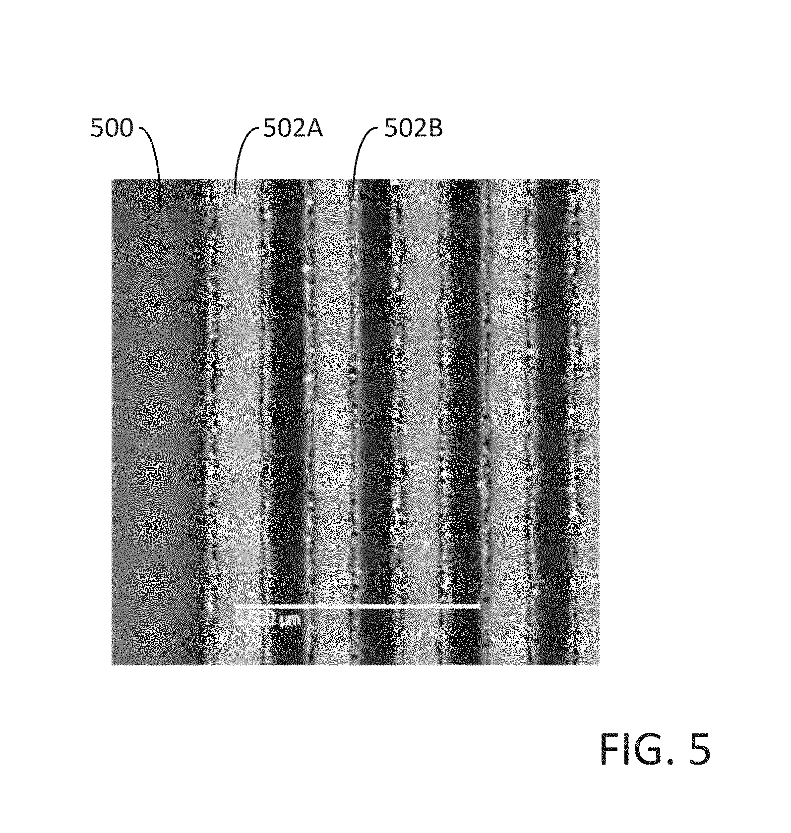
[0089] As a further non-limiting example embodiment of the methods of the current disclosure, FIG. 5 illustrates a partially fabricated semiconductor device structure including a metallic capping layer structure deposited according to the embodiments of the disclosure. In more detail, FIG. 5 illustrates a metallic capping layer structure deposited by selectively depositing the first metallic capping layer by a selective cyclical deposition process, i.e., the methods outlined by the process flow of FIG. 2A and FIG. 2C. FIG. 5 illustrates a partially fabricated semiconductor device structure comprising a dielectric material 500 and a selectively deposit tungsten capping layer structure 502, the tungsten capping layer structure being disposed over a copper interconnect (e.g., tungsten region 502A) and over a tantalum barrier (e.g., tungsten region 502B). In the embodiment illustrated in FIG. 5, the first metallic capping layer was depositing by a selective cyclical deposition process comprising alternating exposure of the partially fabricated semiconductor device structure to tungsten hexafluoride (WF.sub.6) and hydrogen (H.sub.2). The selective cyclical deposition process was carried for a total number of 50 deposition cycles followed by the selective CVD of tungsten utilizing tungsten hexafluoride (WF.sub.6) and hydrogen (H.sub.2). As illustrated in FIG. 5, the selective deposition process results in no deposition over the dielectric material, indicating a selective deposition process with 100% selectivity to the metallic regions relative to the dielectric regions.
[0090] The embodiments of the current disclosure may also provide semiconductor device structures, such as, for example, the semiconductor device structure 318 of FIG. 3C. In more detail, the semiconductor device structure 318 may comprise a substrate 302 which may comprise one or more materials including, but not limited to, silicon, silicon germanium (Si.sub.1-xGe.sub.x), silicon germanium tin (Si.sub.xGe.sub.1-xSn.sub.y), germanium, silicon carbide, and III-V semiconductors. Although not illustrated in FIG. 3C, the substrate 302 may include one or more semiconductor device structures formed into or onto a surface of the substrate 302. For example, the substrate may comprise partially fabricated and/or fabricated semiconductor device structures such as transistors and memory elements.
[0091] The semiconductor device structure 318 of FIG. 3C, may further comprise a dielectric material 304 disposed over the substrate 302, and in some embodiments, the dielectric material 304 may be disposed directly over the substrate 302. In some embodiments, the dielectric material 304 may comprise a low dielectric constant material, i.e., a low-k material, which may be defined as a dielectric material having a dielectric constant less than about 4.0. In some embodiments, the dielectric constant of the low-k material may be less than 3.5, or less than 3.0, or less than 2.5, or even less than 2.3. In some embodiments, the dielectric material 304 may comprise a silicon containing dielectric material, including, but not limited to, a silicon oxide, a silicon nitride, a silicon oxynitride, or mixtures thereof. In some embodiments, the dielectric material 304 may comprise a metal oxide material, including, but not limited to, a titanium oxide, a tantalum oxide, or an aluminum oxide.
[0092] The semiconductor device structure 318 of FIG. 3C, may also comprise a trench structure disposed in the dielectric material 304, the trench structure extending from the upper exposed surface of the dielectric material 304 and at least partially into the dielectric material 304. In some embodiments, the trench structure may extend from the upper exposed surface of the dielectric material 304 to the substrate 302. In some embodiment of the disclosure, the trench structure disposed within the dielectric material 304 may be lined with a metallic barrier material 306, i.e., a metallic barrier material 306 may be directly in contact with the dielectric material 304 in the trench structure. In some embodiments, the metallic barrier material 306 may comprise an elemental metal, or a metal nitride. In some embodiments, the metallic barrier material 306 may comprise at least one of tantalum, tantalum nitride, titanium, titanium nitride, ruthenium or manganese.
[0093] In some embodiments of the disclosure, the semiconductor device structure 318 may also comprise a metallic interconnect material 308 which may be disposed in the trench structure and in direct contact with the metallic barrier material 306. In some embodiments, the metallic interconnect material 308 may comprise at least one of copper (Cu), or cobalt (Co).
[0094] In some embodiments of the disclosure, the semiconductor device structure 318 of FIG. 3C may further comprise a capping layer structure 316. The capping layer structure 316 may be disposed directly over the upper surface of the metallic interconnect material 308 and over the upper surface of the metallic barrier material 306. In some embodiments, the capping layer structure 316 may be disposed in the trench structure formed in the dielectric material 304. In some embodiments, the capping layer structure 316 may comprise a first metallic capping layer 310 and a second metallic capping layer 314, wherein the second metallic capping layer 314 is disposed directly on the first metallic capping layer 310. In some embodiments of the disclosure, the first metallic capping layer 310 may comprise at least one of tungsten, titanium, titanium nitride, tantalum, or tantalum nitride. In some embodiments, the first metallic capping layer 310 may have a thickness of less than 50 Angstroms, or less than 30 Angstroms, or even less than 20 Angstroms. In some embodiments of the disclosure, the second metallic capping layer 314 may comprise at least one of tungsten, titanium, titanium nitride, tantalum, or tantalum nitride. In some embodiments, the second metallic capping layer 314 may have a thickness of less than 120 Angstroms, or less than 60 Angstroms, or even less than 30 Angstroms. In some embodiments, the first metallic capping layer 310 and the second metallic capping layer 314 may comprise the same material, whereas in alternative embodiments, the first metallic capping layer 310 and the second metallic capping layer 314 may comprise different materials.
[0095] The example embodiments of the disclosure described above do not limit the scope of the invention, since these embodiments are merely examples of the embodiments of the invention, which is defined by the appended claims and their legal equivalents. Any equivalent embodiments are intended to be within the scope of this invention. Indeed, various modifications of the disclosure, in addition to those shown and described herein, such as alternative useful combination of the elements described, may become apparent to those skilled in the art from the description. Such modifications and embodiments are also intended to fall within the scope of the appended claims.
* * * * *
D00000
D00001
D00002
D00003
D00004
D00005
D00006
D00007
D00008
XML
uspto.report is an independent third-party trademark research tool that is not affiliated, endorsed, or sponsored by the United States Patent and Trademark Office (USPTO) or any other governmental organization. The information provided by uspto.report is based on publicly available data at the time of writing and is intended for informational purposes only.
While we strive to provide accurate and up-to-date information, we do not guarantee the accuracy, completeness, reliability, or suitability of the information displayed on this site. The use of this site is at your own risk. Any reliance you place on such information is therefore strictly at your own risk.
All official trademark data, including owner information, should be verified by visiting the official USPTO website at www.uspto.gov. This site is not intended to replace professional legal advice and should not be used as a substitute for consulting with a legal professional who is knowledgeable about trademark law.