Optoelectronic Component
MEISTER; Stefan ; et al.
U.S. patent application number 15/515923 was filed with the patent office on 2019-05-16 for optoelectronic component. This patent application is currently assigned to TECHNISCHE UNIVERSITAT BERLIN. The applicant listed for this patent is TECHNISCHE UNIVERSITAT BERLIN. Invention is credited to Sebastian KUPIJAI, Stefan MEISTER, Hanjo RHEE, Christoph THEISS.
| Application Number | 20190146151 15/515923 |
| Document ID | / |
| Family ID | 54883942 |
| Filed Date | 2019-05-16 |


View All Diagrams
| United States Patent Application | 20190146151 |
| Kind Code | A1 |
| MEISTER; Stefan ; et al. | May 16, 2019 |
OPTOELECTRONIC COMPONENT
Abstract
The invention relates to an optoelectronic component (100) comprising a chip (110) comprising a substrate (12) and at least one optical waveguide (20) integrated in the chip (110). In one variant of the invention it is provided that an electro-optical component (30) is monolithically integrated in one or a plurality of semiconductor layers of the chip (110) arranged on the substrate top side (12a) of the substrate (12), or on the substrate top side (12a) of the substrate (12) and at least one electrical connection of the monolithically integrated electro-optical component (30) is connected by means of a connection line (41) to a conductor track connection (43) situated below the substrate rear side (12b), wherein the connection line (41) extends through a through hole (42) in the substrate (12) from the electro-optical component (30) to the conductor track connection (43) situated below the substrate rear side (12b).
| Inventors: | MEISTER; Stefan; (Berlin, DE) ; RHEE; Hanjo; (Berlin, DE) ; THEISS; Christoph; (Berlin, DE) ; KUPIJAI; Sebastian; (Berlin, DE) | ||||||||||
| Applicant: |
|
||||||||||
|---|---|---|---|---|---|---|---|---|---|---|---|
| Assignee: | TECHNISCHE UNIVERSITAT
BERLIN Berlin DE |
||||||||||
| Family ID: | 54883942 | ||||||||||
| Appl. No.: | 15/515923 | ||||||||||
| Filed: | September 28, 2015 | ||||||||||
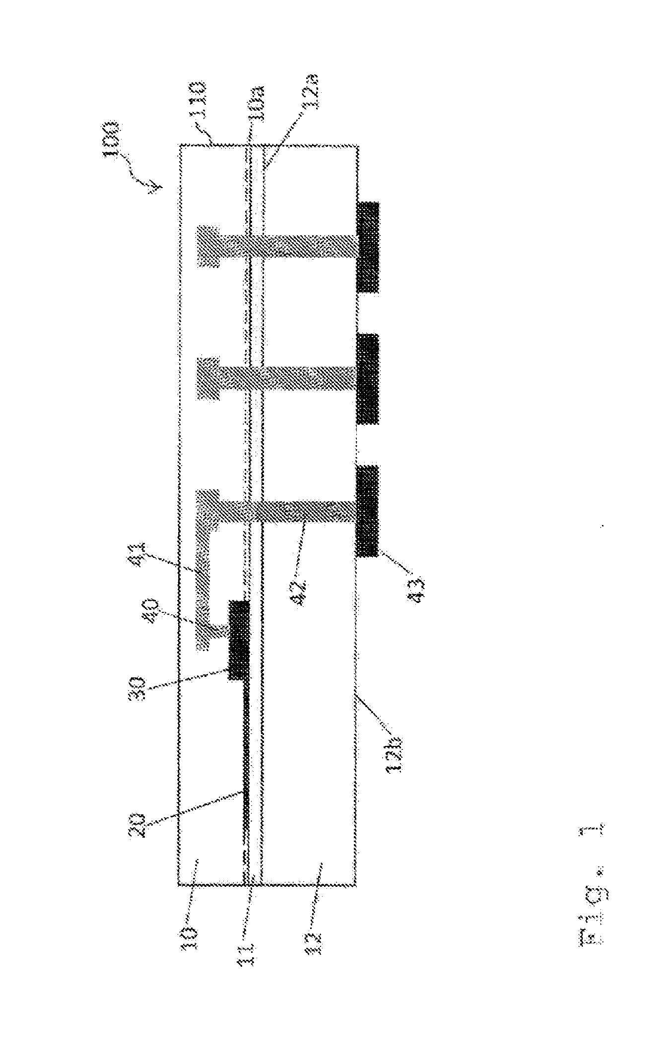
| PCT Filed: | September 28, 2015 | ||||||||||
| PCT NO: | PCT/DE2015/200464 | ||||||||||
| 371 Date: | March 30, 2017 |
| Current U.S. Class: | 385/14 |
| Current CPC Class: | G02B 6/12004 20130101; G02B 6/4274 20130101; G02B 2006/12107 20130101; G02B 6/428 20130101; G02B 6/4214 20130101; G02B 6/43 20130101; G02B 6/30 20130101 |
| International Class: | G02B 6/12 20060101 G02B006/12; G02B 6/42 20060101 G02B006/42; G02B 6/30 20060101 G02B006/30; G02B 6/43 20060101 G02B006/43 |
Foreign Application Data
| Date | Code | Application Number |
|---|---|---|
| Sep 30, 2014 | DE | 10 2014 219 792.9 |
Claims
1. An optoelectronic component (100) comprising a chip (110) comprising a substrate (12) and at least one optical waveguide (20) integrated in the chip (110), characterized in that an electro-optical component (30) is monolithically integrated in one or a plurality of semiconductor layers of the chip (110) arranged on the substrate top side (12a) of the substrate (12), or on the substrate top side (12a) of the substrate (12) and at least one electrical connection of the monolithically integrated electro-optical component (30) is connected by means of a connection line (41) to a conductor track connection (43) situated below the substrate rear side (12b), wherein the connection line (41) extends through a through hole (42) in the substrate (12) from the electro-optical component (30) to the conductor track connection (43) situated below the substrate rear side (12b).
2. The optoelectronic component (100) as claimed in claim 1, characterized in that at least one of the optical connections, preferably all of the optical connections, are arranged on the chip top side of the chip (110) and at least one of the electrical connections, preferably all of the electrical connections, are arranged on the chip underside of the chip (110).
3. The optoelectronic component (100) as claimed in claim 1, characterized in that the monolithically integrated electro-optical component (30) is a photodetector (32) or a modulator (31).
4. The optoelectronic component (100) as claimed in claim 1, characterized in that the integrated waveguide (20) is equipped with or connected to a deflection device which deflects optical radiation to be coupled out from the waveguide (20) virtually perpendicularly in the direction of the chip top side, or deflects radiation incident virtually perpendicularly from the chip top side and couples it into the waveguide (20).
5. The optoelectronic component (100) as claimed in claim 4, characterized in that the deflection device is formed by a grating coupler (21) embodied in the waveguide (20).
6. The optoelectronic component (100) as claimed in claim 1, characterized in that a silicon dioxide layer is situated on the substrate (12) and a silicon layer (10a) is situated above said silicon dioxide layer, and the optical waveguide (20) and the electro-optical component (30) are monolithically integrated in the silicon layer (10a).
7. The optoelectronic component (100) as claimed in claim 1, characterized in that an electrical component (50) is monolithically integrated in one or a plurality of semiconductor layers of the chip (110) arranged on the substrate top side (12a) of the substrate (12) or on the substrate top side (12a) of the substrate (12) and at least one electrical connection of the monolithically integrated electrical component (50) is connected by means of a connection line (41) to a conductor track connection (43) situated below the substrate rear side (12b).
8. The optoelectronic component (100) as claimed in claim 7, characterized in that the monolithically integrated electrical component (50) is an amplifier or a driver.
9. The optoelectronic component (100) as claimed in claim 1, characterized in that the at least one integrated waveguide (20) or at least one of the integrated waveguides (20) in the region of one of its waveguide ends is equipped with or connected to a deflection device by which optical radiation that comes from a light source arranged on the chip top side of the chip (110) and is incident virtually perpendicularly to the chip top side is coupled into the waveguide (20), and in the region of the other waveguide end is equipped with or connected to a deflection device which deflects optical radiation to be coupled out from the waveguide (20) virtually perpendicularly in the direction of the chip top side, in particular in the direction of an optical fiber arranged on the chip top side or in the direction of a light deflection element arranged on the chip top side, wherein at least one electrical connection of the light source is connected by means of a connection line (41) to a conductor track connection (43) situated below the substrate rear side (12b).
10. The optoelectronic component (100) as claimed in claim 9, characterized in that a modulator is monolithically integrated between the two waveguide ends in the chip (110), said modulator modulating the radiation of the light source before coupling into the optical fiber.
11. The optoelectronic component (100) as claimed in claim 1, characterized in that the at least one integrated waveguide (20) or at least one of the integrated waveguides (20) the region of one of its waveguide ends is equipped with or connected to a deflection device by which optical radiation that comes from an optical fiber arranged on the chip top side and is incident virtually perpendicularly to the chip top side is coupled into the waveguide (20), and in the region of the other waveguide end is connected to a photodetector (32) integrated in the chip (110).
12. The optoelectronic component (100) as claimed in claim 11, characterized in that a transimpedance amplifier is monolithically integrated in the chip (110), said transimpedance amplifier amplifying the electrical signal of the photodetector (32).
13. The optoelectronic component (100) as claimed in claim 1, characterized in that the chip (110) is placed by its underside on a printed circuit board that forms a wiring plane for the electrical conductor track connection (43) situated on the chip rear side.
14. The optoelectronic component (100) as claimed in claim 1, characterized in that an electrical component (50) is monolithically integrated in one or a plurality of semiconductor layers of the chip (110) arranged on the substrate top side (12a) of the substrate (12) or on the substrate top side (12a) of the substrate (12), at least one electrical connection of the monolithically integrated electrical component (50) is connected by means of a connection line (41a) to a conductor track connection (43a) situated below the substrate rear side (12b), wherein the connection line (41a) extends through a through hole (42) in the substrate (12) from the electro-optical component (30) to the conductor track connection (43) situated below the substrate rear side (12b), the chip (110) is placed by its underside on a printed circuit board (610) that forms a wiring plane for the electrical conductor track connections (43, 43a) situated on the substrate rear side (12b), and the printed circuit board (610) has at least one connection line (46) which electrically interconnects the conductor track connection (43b) connected to the electrical component (50) and the conductor track connection (43) connected to the electro-optical component (30).
15. An optoelectronic component (100) comprising a chip (110) comprising a substrate (12) and at least one optical waveguide (20) integrated in the chip (110), characterized in that an electrical component (50) is monolithically integrated in one or a plurality of semiconductor layers of the chip (110) arranged on the substrate top side (12a) of the substrate (12), or on the substrate top side (12a) of the substrate (12) and at least one electrical connection of the monolithically integrated electrical component (50) is connected by means of a connection line (41a) to a conductor track connection (43a) situated below the substrate rear side (12b), wherein the connection line (41a) extends through a through hole (42) in the substrate (12) from the electrical component (50) to the conductor track connection (43a) situated below the substrate rear side (12b).
16. The optoelectronic component (100) as claimed in claim 15, characterized in that an electro-optical component (30) is monolithically integrated in one or a plurality of semiconductor layers of the chip (110) arranged on the substrate top side (12a) of the substrate (12) or on the substrate top side (12a) of the substrate (12) and the electro-optical component (30) and the electrical component (50) are connected by means of a line (620) that is arranged on the substrate top side (12a) of the substrate (12).
Description
[0001] The invention relates to optoelectronic components which comprise a chip comprising a substrate and at least one optical waveguide integrated in the chip.
[0002] Optical transceivers, this being the term used by those skilled in the art, obtainable nowadays serve as transmitters and receivers for converting electrical data signals into electrical signals, and vice versa. The main difficulty is that an integrated assembly, referred to as "package" by those skilled in the art, for an optical transceiver firstly has to provide the photonic integrated circuits, consisting of waveguides, optically active components and optically passive components, such as modulators, photodiodes, splitters and light couplers. Secondly, electronic components such as modulator driver, transimpedance amplifier (TIA), limiting amplifier (LA), this being the term used by those skilled in the art, clock and data recovery (CDR), this being the term used by those skilled in the art, and equalizer, this being the term used by those skilled in the art, are necessary, for which highly developed connection techniques from microelectronics already exist. The intention is to accommodate this multiplicity of different components in a common form factor as compactly as possible and in a manner that saves as much energy as possible, in conjunction with low electrical and optical losses and using cost-effective construction technology. At the same time, an efficient scalability toward higher transmission rates and quantities must be part of the overall concept.
[0003] As is known, the individual chips of the transceiver can be applied and electrically contacted by wire bonding, this being the term used by those skilled in the art, or by installation upside down without bonding wires, referred to as "flip chip" by those skilled in the art, on a wiring substrate, referred to as "interposer" by those skilled in the art, which consists e.g. of silicon, ceramic or a polymer, or directly on a substrate that usually consists of a printed circuit board (PCB). In this context there are variants in which the optical fibers are led through an opening in the wiring substrate or substrate to the optical chip [1, 2] or from above into a region that is free of electrical contact pads. Solutions are likewise being developed in which optical signals are coupled into a wiring substrate [3], or in some concepts into a substrate [1], are guided there and are coupled out again therefrom. The considerable disadvantage here is the long signal paths with corresponding damping losses and coupling losses at each transition. These additional losses by themselves may have the consequence that the end-to-end power budget for the entire transmission link leaves no more margin for the losses that can occur in the actual transmission medium, generally an optical fiber.
[0004] Present-day commercial optical transceivers, usually based on signal transmission in multimode fibers, comprise diverse discrete optical components for beam deflection and shaping, such as microlenses, microprisms, beam splitters and deflection mirrors. These components have to be positioned and fixed on a carrier by machine, which obstructs simple scalability.
[0005] Proceeding from the prior art described, the invention is based on the object of specifying an optoelectronic component which has a simple and cost-effective overall construction.
[0006] This object is achieved according to the invention by means of an optoelectronic component having the features as claimed in patent claim 1. Advantageous configurations of the optoelectronic component according to the invention are specified in dependent claims.
[0007] Accordingly, it is provided according to the invention that an electro-optical component is monolithically integrated in one or a plurality of semiconductor layers of the chip arranged on the substrate top side of the substrate, or on the substrate top side of the substrate and at least one electrical connection of the monolithically integrated electro-optical component is connected by means of a connection line to a conductor track connection situated below the substrate rear side, wherein the connection line extends through a through hole in the substrate from the electro-optical component to the conductor track connection situated below the substrate rear side.
[0008] A major advantage of the component according to the invention or of the component construction according to the invention is that a separation between the optical connection side and the electrical connection side is achievable. In this regard, by way of example, the optical connection side can be arranged on the chip top side of the chip and the electrical connection side can be arranged on the chip underside of the chip.
[0009] It is thus particularly advantageous if at least one of the optical connections, preferably all of the optical connections, are arranged on the chip top side of the chip and at least one of the electrical connections, preferably all of the electrical connections, are arranged on the chip underside of the chip.
[0010] The monolithically integrated electro-optical component is preferably a photodetector or a modulator.
[0011] Preferably, the integrated waveguide is equipped with or connected to a deflection device which deflects optical radiation to be coupled out from the waveguide virtually perpendicularly in the direction of the chip top side, or deflects radiation incident virtually perpendicularly from the chip top side and couples it into the waveguide.
[0012] The deflection device is preferably formed by a grating coupler embodied in the waveguide.
[0013] SOI (Silicon-On-Insulator) material is preferably used as chip base material. Accordingly, it is considered to be advantageous if a silicon dioxide layer is situated on the substrate and a silicon cover layer is situated above said silicon dioxide layer, and the optical waveguide and the electro-optical component are integrated in the silicon cover layer.
[0014] Moreover, it is advantageous if an electrical component is monolithically integrated in one or a plurality of semiconductor layers of the chip arranged on the substrate top side of the substrate or on the substrate top side of the substrate and at least one electrical connection of the monolithically integrated electrical component is connected by means of a connection line to a conductor track connection situated below the substrate rear side.
[0015] The monolithically integrated electrical component is preferably an amplifier or a driver.
[0016] In one particularly preferred configuration of the optoelectronic component it is provided that the at least one integrated waveguide or at least one of the integrated waveguides in the region of one of its waveguide ends is equipped with or connected to a deflection device by which optical radiation that comes from a light source arranged on the chip top side of the chip and is incident virtually perpendicularly to the chip top side is coupled into the waveguide, and in the region of the other waveguide end is equipped with or connected to a deflection device which deflects optical radiation to be coupled out from the waveguide virtually perpendicularly in the direction of the chip top side, in particular in the direction of an optical fiber arranged on the chip top side or in the direction of a light deflection element arranged on the chip top side. At least one electrical connection of the light source is preferably connected by means of a connection line to a conductor track connection situated below the substrate rear side. The deflection devices arranged in the region of the waveguide ends are preferably Bragg gratings that are introduced in the waveguide.
[0017] Preferably, a modulator is monolithically integrated between the two waveguide ends in the chip, said modulator modulating the radiation of the light source before coupling into the optical fiber.
[0018] Moreover, it is advantageous if the at least one integrated waveguide or at least one of the integrated waveguides in the region of one of its waveguide ends is equipped with or connected to a deflection device by which optical radiation that comes from an optical fiber arranged on the chip top side and is incident virtually perpendicularly to the chip top side is coupled into the waveguide, and in the region of the other waveguide end is connected to a photodetector monolithically integrated in the chip. The deflection device arranged in the region of the waveguide end is preferably a Bragg grating that is introduced in the waveguide.
[0019] Preferably, in addition a transimpedance amplifier is monolithically integrated in the chip, said transimpedance amplifier amplifying the electrical signal of the photodetector.
[0020] Moreover, it is advantageous if the chip is placed by its underside on a printed circuit board that forms a wiring plane for the electrical conductor track connection situated on the chip rear side.
[0021] In a further advantageous configuration of the optoelectronic component it is provided that an electrical component is monolithically integrated in one or a plurality of semiconductor layers of the chip arranged on the substrate top side of the substrate or on the substrate top side of the substrate, at least one electrical connection of the monolithically integrated electrical component is connected by means of a connection line to a conductor track connection situated below the substrate rear side, wherein the connection line extends through a (dedicated) through hole in the substrate from the electro-optical component to the conductor track connection situated below the substrate rear side, and the chip is placed by its underside on a printed circuit board that forms a wiring plane for the electrical conductor track connections situated on the substrate rear side. The printed circuit board preferably has at least one connection line which electrically interconnects the conductor track connection connected to the electrical component and the conductor track connection connected to the electro-optical component.
[0022] An optoelectronic component comprising a chip comprising a substrate and at least one optical waveguide integrated in the chip is additionally regarded as an invention, wherein it is provided that an electrical component is monolithically integrated in one or a plurality of semiconductor layers of the chip arranged on the substrate top side of the substrate, or on the substrate top side of the substrate and at least one electrical connection of the monolithically integrated electrical component is connected by means of a connection line to a conductor track connection situated below the substrate rear side, wherein the connection line extends through a through hole in the substrate from the electrical component to the conductor track connection situated below the substrate rear side.
[0023] Preferably, an electro-optical component is additionally monolithically integrated in one or a plurality of semiconductor layers of the chip arranged on the substrate top side of the substrate or on the substrate top side of the substrate. The electro-optical component and the electrical component are preferably connected by means of a line that is arranged on the substrate top side of the substrate.
[0024] The invention is explained in greater detail below on the basis of exemplary embodiments with reference to FIGS. 1 to 17.
[0025] FIG. 1 shows in cross section one exemplary embodiment of an optoelectronic component 100 comprising a chip 110, preferably in the form of an SOT chip. The chip 110 comprises a substrate 12 in the form of a silicon substrate, a buried silicon dioxide layer 11 situated on the top side 12a of the substrate 12, a silicon layer 10a situated on the silicon dioxide layer 11, and a material layer assembly 10 situated on the silicon layer 10a. The material layer assembly 10 forms in the jargon the so-called "backend of line" region of the chip 110.
[0026] An optical waveguide 20 is integrated in the chip 110, said optical waveguide preferably being a ridge waveguide embodied in the silicon layer 10a. In addition, an electro-optical component 30 is monolithically integrated in the chip 110, preferably in the silicon layer 10a. The electro-optical component 30 is connected by means of a connection line 41 to a conductor track connection 43 situated below the substrate rear side 12b. The connection line 41 extends through a through hole 42 in the substrate 12 from the electro-optical component 30 to the conductor track connection 43 situated below the substrate rear side 12b.
[0027] The connection line 41 can, in sections, bear on the chip top side of the chip 110 or--as shown in FIG. 1--be integrated within the material layer assembly 10. In both cases, a section of the connection line 41 preferably extends through a hole 40 in the material layer assembly 10 or in the "backend of line" region of the chip 110 or through a hole 40 in one or more layers of said material layer assembly 10 in the direction of the chip top side of the chip 110.
[0028] FIG. 2 shows the optoelectronic component 100 in accordance with FIG. 1 in plan view.
[0029] FIG. 3 shows in plan view a further exemplary embodiment of an optoelectronic component 100 comprising a chip 110 in the form of an SOI chip. An optical waveguide 20, a grating coupler 21 and also an electrical component in the form of control electronics 50 are monolithically integrated into the silicon layer 10a (see FIG. 1) of the chip 110 that is situated on the buried silicon dioxide layer 11 (see FIG. 1). For the rest, the above explanations in association with FIGS. 1 and 2 are correspondingly applicable.
[0030] Further preferred exemplary embodiments of optoelectronic components are shown in FIGS. 4 to 13.
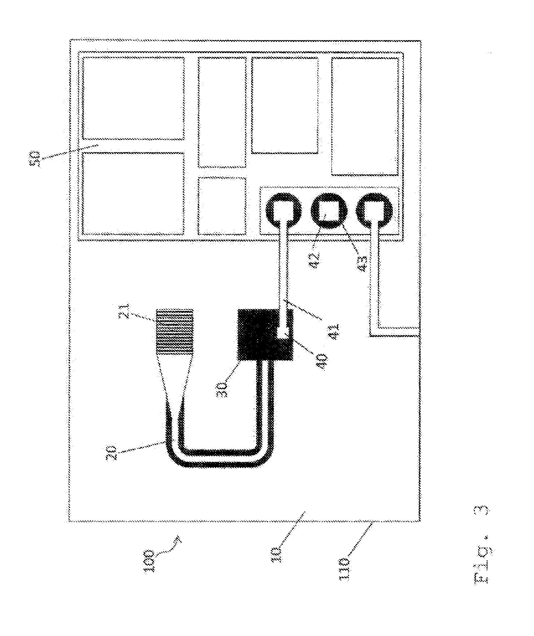
[0031] FIG. 4 shows in cross section one exemplary embodiment of an optoelectronic component 100 which is positioned with further components on a wiring substrate 61 and is sealed with potting material 60. The wiring substrate 61 is connected to the carrier substrate 62 via connections for electrical contacting 65. Alongside the optoelectronic component 100, one or a plurality of electronic chips 63 are situated on the wiring substrate 61, said electronic chips being connected to the wiring substrate 61 via electrical contactings 64.
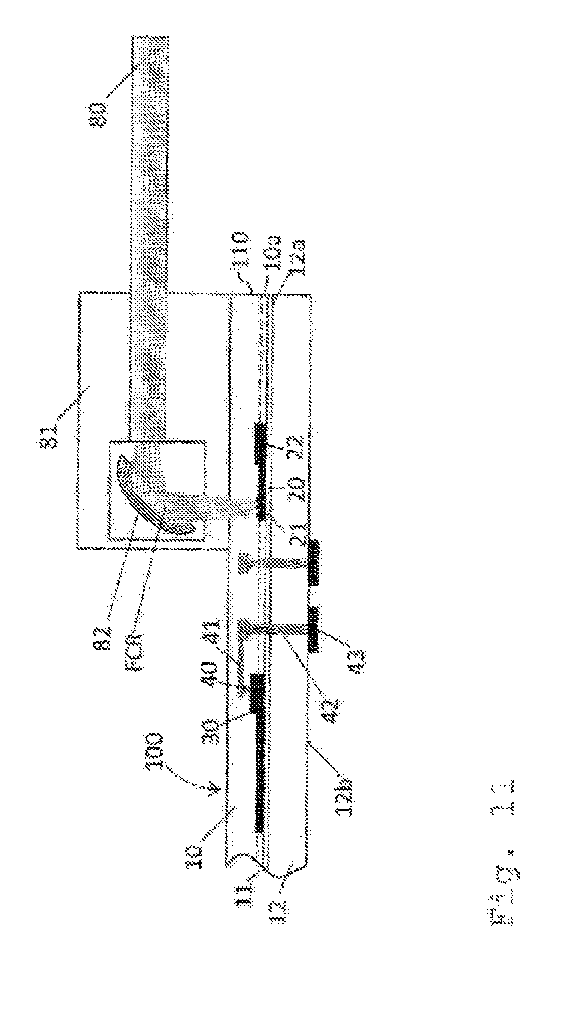
[0032] Situated on the top side of the chip 110 in the "backend of line" region 10 is one or a plurality of monolithically integrated lenses 23 for the optical coupling of the emerging optical radiation LOR of one or a plurality of lasers 70 situated on the optoelectronic component 100, said lasers being connected via electrical contactings 45 to the through holes 42 in the chip 110.
[0033] One or a plurality of optical fibers 80 are connected to plugs 81 fitted on the optoelectronic component 100, said plugs containing deflection optical units 82, in a manner such that the optical fiber or fibers 80 run(s) parallel to the chip top side 110. The optical radiation FCR deflected by the deflection optical units 2 is coupled to one or a plurality of waveguides 20 via deflection units such as e.g. grating couplers 21 and is processed e.g. in a monolithically integrated electro-optical component 30.
[0034] FIG. 5 shows in cross section one exemplary embodiment of an optoelectronic component 100 in which one or a plurality of lasers 70 are situated alongside the optoelectronic component 100 on the wiring substrate 61 and the emerging optical radiation LOR is coupled through a lens 24 in or on one or a plurality of lasers 70 and through the adjacent end facet of one or a plurality of waveguides 20 into the chip 110 and is processed e.g. in a monolithically integrated electro-optical component 30.
[0035] FIG. 6 shows in cross section one exemplary embodiment of an optoelectronic component 100 in which the monolithically integrated electro-optical component is a modulator 31.
[0036] FIG. 7 shows the optoelectronic component 100 in accordance with FIG. 6 in plan view.
[0037] FIG. 8 shows in cross section one exemplary embodiment of an optoelectronic component 100 in which the monolithically integrated electro-optical component is a photodetector 32.
[0038] FIG. 9 shows the optoelectronic component 100 in accordance with FIG. 8 in plan view.
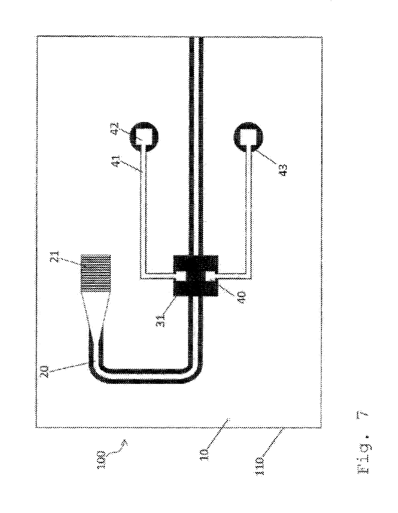
[0039] FIG. 10 shows in cross section one exemplary embodiment of an optoelectronic component 100 in which one or a plurality of optical fibers 80 are connected to plugs 81 fitted on the optoelectronic component 100 in a manner such that the optical fiber or fibers 80 point(s) virtually perpendicularly in the direction of the chip top side 110. The optical radiation FCR is coupled to one or a plurality of waveguides 20 via deflection units such as e.g. grating couplers 21 and is processed e.g. in a passive photonic component 22.
[0040] FIG. 11 shows in cross section one exemplary embodiment of an optoelectronic component 100 in which one or a plurality of optical fibers 80 are connected to plugs 81 fitted on the optoelectronic component 100, said plugs containing deflection optical units 82, in a manner such that the optical fiber or fibers 80 run(s) parallel to the chip top side 110. The optical radiation FCR deflected by the deflection optical units 2 is coupled to one or a plurality of waveguides 20 via deflection units such as e.g. grating couplers 21 and is processed e.g. in a passive photonic component 22.
[0041] FIG. 12 shows in cross section one exemplary embodiment of an optoelectronic component 100 in which one or a plurality of monolithically integrated lenses 23 are situated on the top side of the chip 110 in the "backend of line" region 10, said lenses serving for the optical coupling of the emerging optical radiation LOR of one or a plurality of lasers 70 situated on the optoelectronic component 100, said lasers being connected via electrical contactings 45 to the through holes 42 in the chip 110. The optical radiation LOR emerging from the underside of the laser or lasers 70 is coupled to one or a plurality of waveguides 20 via deflection units such as e.g. grating couplers 21 and is processed e.g. in a monolithically integrated electro-optical component 30.
[0042] FIG. 13 shows in cross section one exemplary embodiment of an optoelectronic component 100 in which one or a plurality of lasers 70 are situated on the optoelectronic component 100, said lasers being connected via electrical contactings 45 to the through holes 42 in the chip 110. The optical radiation LOR emerging laterally from the laser or lasers 70 is guided by a beam deflection 27 in deflection units such as e.g. grating couplers 21 and is coupled to one or a plurality of waveguides 20 and is processed e.g. in a monolithically integrated electro-optical component 30.
[0043] FIG. 14 shows a further exemplary embodiment of an optoelectronic component 100 according to the invention. The component 100 comprises a chip 110 comprising a substrate 12 and at least one optical waveguide 20 integrated in the chip 110.
[0044] An electro-optical component 30 is monolithically integrated in one or a plurality of semiconductor layers of the chip 110 arranged on the substrate top side 12a of the substrate 12, or on the substrate top side 12a of the substrate 12.
[0045] At least one electrical connection of the monolithically integrated electro-optical component 30 is connected by means of a connection line 41 to a conductor track connection 43 situated below the substrate rear side 12b.
[0046] The connection line 41 extends through a through hole 42 in the substrate 12 from the electro-optical component 30 to the conductor track connection 43 situated below the substrate rear side 12b.
[0047] In addition, an electrical component 50 is monolithically integrated in one or a plurality of semiconductor layers of the chip 110 arranged on the substrate top side 12a of the substrate 12, or on the substrate top side 12a of the substrate 12.
[0048] At least one electrical connection of the monolithically integrated electrical component 50 is connected by means of a connection line 41a to a conductor track connection 43a situated below the substrate rear side 12b.
[0049] The connection line 41a extends through a through hole 42a in the substrate 12 from the electrical component 50 to the conductor track connection 43a situated below the substrate rear side 12b.
[0050] The chip 110 is placed by its underside on a printed circuit board 610 that forms a wiring plane for the electrical conductor track connections 43 and 43a situated on the chip rear side or the substrate rear side 12b. The printed circuit board 610 comprises at least one connection line 46 which electrically interconnects the conductor track connection 43a connected to the electrical component 50 and the conductor track connection 43 connected to the electro-optical component 30.
[0051] FIG. 15 shows a further exemplary embodiment of an optoelectronic component 100 according to the invention. The component 100 comprises a chip 110 comprising a substrate 12 and at least one optical waveguide 20 integrated in the chip 110.
[0052] An electro-optical component 30 and an electrical component 50 are monolithically integrated in one or a plurality of semiconductor layers of the chip 110 arranged on the substrate top side 12a of the substrate 12, or on the substrate top side 12a of the substrate 12.
[0053] At least one electrical connection of the monolithically integrated electrical component 50 is connected by means of a connection line 41a to a conductor track connection 43a situated below the substrate rear side 12b.
[0054] The connection line 41a extends through a through hole 42a in the substrate 12 from the electrical component 50 to the conductor track connection 43a situated below the substrate rear side 12b.
[0055] The chip 110 is placed by its underside on a printed circuit board 610 that forms a wiring plane for the electrical conductor track connection 43a situated on the chip rear side or the substrate rear side 12b.
[0056] The printed circuit board 610 comprises at least one connection line 46 which connects the conductor track connection 43a connected to the electrical component 50 to another component (not shown in FIG. 15 for reasons of clarity).
[0057] The electro-optical component 30 and the electrical component 50 are connected by means of at least one line 620 which is arranged on the substrate top side 12a of the substrate 12.
[0058] In the exemplary embodiments in accordance with FIGS. 14 and 15, the electrical component 50 is in each case directly on the substrate 12 and terminates (upward) in each case in terms of height with the waveguides 20 in the silicon layer 10a. In other words, the electrical component 50 extends in each case from the substrate 12 right into the silicon layer 10a situated on the silicon dioxide layer.
[0059] The exemplary embodiments in accordance with FIGS. 16 and 17 respectively correspond to the exemplary embodiments in accordance with FIGS. 14 and 15 apart from the configuration of the electrical component 50. In the exemplary embodiments in accordance with FIGS. 16 and 17, the electrical component 50 is arranged in each case exclusively in the silicon layer 10a; for the rest, the explanations in association with the exemplary embodiments in accordance with FIGS. 14 and are correspondingly applicable for the exemplary embodiments in accordance with FIGS. 16 and 17.
[0060] Although the invention has been more specifically illustrated and described in detail by means of preferred exemplary embodiments, nevertheless the invention is not restricted by the examples disclosed and other variations can be derived therefrom by the person skilled in the art, without departing from the scope of protection of the invention.
LITERATURE
[0061] [1] H. Schroder, T. Bierhoff and D. Craiovan, "Anforderungen und Losungen zur hochprazisen optoelektronischen und mikrooptischen Montage auf Baugruppentragern," Cooperative Computing & Communication Laboratory, C-Lab Report 9, 6, 2010. [0062] [2] F. E. Doany, B. G. Lee, C. L. Schow, C. K. Tsang, C. Baks, Y. Kwark, R. John, J. J. Knickerbocker and J. A. Kash, "Terabit/s-class 24-channel bidirectional optical transceiver module based on TSV Si carrier for board-level interconnects," in ECTC, Electronic Components and Technology Conference, Piscataway, N.J.: IEEE, 2010, pages 58-65. [0063] [3] P. de Dobbelaere, G. Young and M. Peterson, "Method And System For A Photonic Interposer", USA 13/422,776, Jul. 12, 2012.
REFERENCE SIGNS
[0063] [0064] 10 Material layer assembly [0065] 10a Silicon layer [0066] 11 Silicon dioxide layer [0067] 12 Substrate [0068] 12a Top side of the substrate [0069] 12b Substrate rear side [0070] 20 Optical waveguide [0071] 21 Grating coupler [0072] 22 Passive photonic component [0073] 23 Monolithically integrated lens in the "backend of line" region [0074] 24 Lens in or on a laser [0075] 27 Beam deflection [0076] 30 Monolithically integrated electro-optical component [0077] 31 Monolithically integrated electro-optical modulator [0078] 32 Monolithically integrated photodiode/photodetector [0079] 40 Hole [0080] 41 Connection line [0081] 41a Connection line [0082] 42 Through hole [0083] 42a Through hole [0084] 43 Conductor track connection [0085] 43a Conductor track connection [0086] 44 Connection for electrical contacting on a wiring substrate [0087] 45 Connection for electrical contacting of a laser chip [0088] 46 Connection line [0089] 50 Monolithically integrated control electronics (cointegration) [0090] 60 Potting material [0091] 61 Wiring substrate [0092] 62 Carrier substrate (e.g. printed circuit board (PCB)) [0093] 63 Electronic chip [0094] 64 Connection for the electrical contacting of an electronic chip with the wiring substrate [0095] 65 Connection for the electrical contacting of the wiring substrate with the carrier substrate [0096] 70 Laser [0097] 80 Fiber [0098] 81 Fiber plug [0099] 82 Deflection optical unit in the fiber plug [0100] 100 Optoelectronic component [0101] 110 Chip [0102] 610 Printed circuit board [0103] 620 Line
* * * * *
D00000
D00001
D00002
D00003
D00004
D00005
D00006
D00007
D00008
D00009
D00010
D00011
D00012

D00013

D00014

D00015

D00016

D00017

XML
uspto.report is an independent third-party trademark research tool that is not affiliated, endorsed, or sponsored by the United States Patent and Trademark Office (USPTO) or any other governmental organization. The information provided by uspto.report is based on publicly available data at the time of writing and is intended for informational purposes only.
While we strive to provide accurate and up-to-date information, we do not guarantee the accuracy, completeness, reliability, or suitability of the information displayed on this site. The use of this site is at your own risk. Any reliance you place on such information is therefore strictly at your own risk.
All official trademark data, including owner information, should be verified by visiting the official USPTO website at www.uspto.gov. This site is not intended to replace professional legal advice and should not be used as a substitute for consulting with a legal professional who is knowledgeable about trademark law.