Method And Apparatus For Data Transmission
WU; Wei-De ; et al.
U.S. patent application number 16/086557 was filed with the patent office on 2019-05-02 for method and apparatus for data transmission. This patent application is currently assigned to MEDIATEK INC.. The applicant listed for this patent is MEDIATEK INC.. Invention is credited to Ju-Ya CHEN, Tao CHEN, Wei-Jen CHEN, Mao-Ching CHIU, Wei-Nan SUN, Kuo-Ming WU, Wei-De WU.
| Application Number | 20190132087 16/086557 |
| Document ID | / |
| Family ID | 59960516 |
| Filed Date | 2019-05-02 |


| United States Patent Application | 20190132087 |
| Kind Code | A1 |
| WU; Wei-De ; et al. | May 2, 2019 |
METHOD AND APPARATUS FOR DATA TRANSMISSION
Abstract
Aspects of the disclosure provide an apparatus that includes a transceiver circuit and a baseband processing circuit. The transceiver circuit is configured to transmit signals that carry a data unit to another apparatus and receive signals that carry a response from the other apparatus. The baseband processing circuit is configured to provide a first digital stream to carry a data unit to the transceiver circuit for transmission, and provide a second digital stream to carry a portion of the data unit to the transceiver circuit for retransmission when the transceiver circuit receives a response that is indicative of a partial receiving failure of the data unit at the other apparatus.
| Inventors: | WU; Wei-De; (Hsinchu City, TW) ; WU; Kuo-Ming; (Zhubei City, TW) ; CHEN; Ju-Ya; (Kaohsiung City, TW) ; CHEN; Tao; (Beijing, CN) ; CHEN; Wei-Jen; (Taipei City, TW) ; CHIU; Mao-Ching; (Minxiong Township, TW) ; SUN; Wei-Nan; (Zhubei City, TW) | ||||||||||
| Applicant: |
|
||||||||||
|---|---|---|---|---|---|---|---|---|---|---|---|
| Assignee: | MEDIATEK INC. Hsin-Chu City TW |
||||||||||
| Family ID: | 59960516 | ||||||||||
| Appl. No.: | 16/086557 | ||||||||||
| Filed: | April 1, 2017 | ||||||||||
| PCT Filed: | April 1, 2017 | ||||||||||
| PCT NO: | PCT/CN2017/079215 | ||||||||||
| 371 Date: | September 19, 2018 |
Related U.S. Patent Documents
| Application Number | Filing Date | Patent Number | ||
|---|---|---|---|---|
| 62316615 | Apr 1, 2016 | |||
| Current U.S. Class: | 1/1 |
| Current CPC Class: | H04L 5/0055 20130101; H04L 1/1614 20130101; H04W 72/042 20130101; H04L 1/1845 20130101; H04L 1/0045 20130101; H04L 5/0053 20130101; H04L 1/1621 20130101; H04L 1/1671 20130101; H04L 27/2647 20130101; H04W 72/0453 20130101; H04L 27/2649 20130101; H04L 5/0094 20130101 |
| International Class: | H04L 1/16 20060101 H04L001/16; H04L 5/00 20060101 H04L005/00; H04W 72/04 20060101 H04W072/04; H04L 27/26 20060101 H04L027/26 |
Claims
1. An apparatus, comprising: a transceiver circuit configured to transmit signals that carry a data unit to another apparatus and receive signals that carry a response from the other apparatus; and a baseband processing circuit configured to provide a first digital stream to carry a data unit to the transceiver circuit for transmission, and provide a second digital stream to carry a portion of the data unit to the transceiver circuit for retransmission when the transceiver circuit receives a response that is indicative of a partial receiving failure of the data unit at the other apparatus.
2. The apparatus of claim 1, wherein the baseband processing circuit further comprises: a transmit processing circuit configured to receive the data unit for transmission, segment the data unit to generate sub data units, and process the sub data units to generate the first digital stream including symbols for the sub data units; and a retransmission control circuit configured to provide control signals to the transmit processing circuit to generate the second digital stream including a subset of the sub data units in response to the partial receiving failure.
3. The apparatus of claim 2, wherein the retransmission control circuit is configured to provide the control signals to the transmit processing circuit to generate the second digital stream including the sub data units when the response includes a single negative acknowledgement bit indicative of a receiving failure of the data unit.
4. The apparatus of claim 2, wherein the retransmission control circuit is configured to determine the subset of the sub data units when the response includes one or multiple negative acknowledgement bit(s) indicative of specific sub data unit(s) with receiving failure.
5. The apparatus of claim 2, wherein the retransmission control circuit is configured to vary the control signals based on the response to adjust a size of the subset of the sub data units to be included in the second digital stream.
6. A method for communication, comprising: generating, by a first apparatus, a first digital steam to carry a data unit for transmission; transmitting, wireless signals in response to the first digital stream to carry the data unit to a second apparatus; receiving, by the first apparatus, wireless signals that carry a response indicative of a partial receiving failure of the data unit from the second apparatus; generating, by the first apparatus, a second digital stream to carry a portion of the data unit; and transmitting, wireless signals in response to the second digital stream to carry the portion of the data unit to the second apparatus.
7. The method of claim 6, wherein generating, by the first apparatus, the first digital stream to carry the data unit for transmission further comprises: segmenting the data unit to generate sub data units; and processing the sub data units to generate the first digital stream including symbols for the sub data units.
8. The method of claim 7, wherein generating, by the first apparatus the second digital stream to carry the portion of the data unit further comprises: generating the second digital stream including a subset of the sub data units in response to the partial receiving failure.
9. The method of claim 8, wherein generating the second digital stream including a subset of the sub data units in response to the partial receiving failure generating the second digital stream including the sub data units when the response includes a single negative acknowledgement bit indicative of a receiving failure of the data unit.
10. The method of claim 8, further comprising: determining the subset of the sub data units when the response includes one or multiple negative acknowledgement bit(s) indicative of specific sub data unit(s) with receiving failure.
11. An apparatus, comprising: a transceiver circuit configured to receive signals transmitted from another apparatus, generate digital samples in response to the received signals and transmit signals that carry a response to the other apparatus; and a baseband processing circuit configured to receive first digital samples from the transceiver circuit that carry a data unit, detect a partial receiving failure of the data unit, cause the transceiver circuit to transmit a response indicative of the partial receiving failure, receive second digital samples from the transceiver circuit that carry a portion of the data unit, and reconstruct the data unit based on the first digital samples and the second digital samples.
12. The apparatus of claim 11, wherein the baseband processing circuit further comprises: a receive processing circuit configured to receive the first digital samples and the second digital samples from the transceiver circuit, extract received first sub data units from the first digital samples and received second sub data units from the second digital samples and detect receiving errors in the received first sub data units and the received second sub data units; and a receive controller configured to construct the data unit based on the first received sub data units and the second received sub data units.
13. The apparatus of claim 12, wherein baseband processing circuit further comprises: a response generator configured to include a single negative acknowledgement bit indicative of a receiving failure of the data unit in the response.
14. The apparatus of claim 12, wherein baseband processing circuit further comprises: a response generator configured to include one or multiple negative acknowledgement bit(s) indicative of specific sub data unit(s) with receiving failure.
15. The apparatus of claim 12, wherein the constructed data unit is input to a data link layer of a protocol stack as a transport block.
16. A method for communication, comprising: receiving, by an apparatus, first wireless signals transmitted from another apparatus, the first wireless signals carrying a data unit; generating first digital samples in response to the received first wireless signals; detecting a partial receiving failure of the data unit; transmitting wireless signals that carry a response indicative of the partial receiving failure; receiving, by the apparatus, second wireless signals transmitted from the other apparatus, the second wireless signals carrying a portion of the data unit; generating second digital samples in response to the received second wireless signals; and reconstructing the data unit based on the first digital samples and the second digital samples.
17. The method of claim 16, further comprising: extracting received first sub data units from the first digital samples; detecting receiving errors in the received first sub data units; extracting received second sub data units from the second digital samples; and constructing the data unit based on the first received sub data units and the second received sub data units.
18. The method of claim 16, wherein transmitting the wireless signals that carry the response indicative of the partial receiving failure further comprises: transmitting the wireless signals that carry the response having a single negative acknowledgement bit indicative of a receiving failure of the data unit.
19. The method of claim 16, wherein transmitting the wireless signals that carry the response indicative of the partial receiving failure further comprises: transmitting the wireless signals that carry the response having one or multiple negative acknowledgement bit(s) indicative of specific sub data unit(s) with receiving failure.
20. The method of claim 16, wherein the constructed data unit is input to a data link layer of a protocol stack as a transport block.
Description
INCORPORATION BY REFERENCE
[0001] This present disclosure claims the benefit of U.S. Provisional Application No. 62/316,615, "Data Channel and Control Channel Enhancement for Wireless Network" filed on Apr. 1, 2016, which is incorporated herein by reference in its entirety.
BACKGROUND
[0002] The background description provided herein is for the purpose of generally presenting the context of the disclosure. Work of the presently named inventors, to the extent the work is described in this background section, as well as aspects of the description that may not otherwise qualify as prior art at the time of filing, are neither expressly nor impliedly admitted as prior art against the present disclosure.
[0003] In wireless communication, electromagnetic signals are used to transmit digital data. The digital data may be incorrectly delivered due to various reasons. In an example, some bits in the digital data can get corrupted due to for example, noise, signal distortion, interference, and the like.
SUMMARY
[0004] Aspects of the disclosure provide an apparatus that includes a transceiver circuit and a baseband processing circuit. The transceiver circuit is configured to transmit signals that carry a data unit to another apparatus and receive signals that carry a response from the other apparatus. The baseband processing circuit is configured to provide a first digital stream to carry a data unit to the transceiver circuit for transmission, and provide a second digital stream to carry a portion of the data unit to the transceiver circuit for retransmission when the transceiver circuit receives a response that is indicative of a partial receiving failure of the data unit at the other apparatus.
[0005] According to an aspect of the disclosure, the baseband processing circuit includes a transmit processing circuit and a retransmission control circuit. The transmit processing circuit is configured to receive the data unit for transmission, segment the data unit to generate sub data units, and process the sub data units to generate the first digital stream including symbols for the sub data units. The retransmission control circuit is configured to provide control signals to the transmit processing circuit to generate the second digital stream including a subset of the sub data units in response to the partial receiving failure.
[0006] In an embodiment, the retransmission control circuit is configured to provide the control signals to the transmit processing circuit to generate the second digital stream including the sub data units when the response includes a single negative acknowledgement bit indicative of a receiving failure of the data unit.
[0007] In another embodiment, the retransmission control circuit is configured to determine the subset of the sub data units when the response includes one or multiple negative acknowledgement bit(s) indicative of a group of sub data unit(s) with receiving failure.
[0008] According to an aspect of the disclosure, the retransmission control circuit is configured to vary the control signals based on the response to adjust a size of the group of the sub data units to be included in the second digital stream.
[0009] In an embodiment, the data unit is a transport block output from a data link layer, and the sub data units are code blocks that are respectively processed by the transmit processing circuit.
[0010] According to an aspect of the disclosure, the retransmission control circuit is also configured to provide control signals to the transmit processing circuit to generate the second digital stream including the subset of the sub data units and additional sub data units for another data unit.
[0011] Aspects of the disclosure provide a method for communication. The method includes generating, by a first apparatus, a first digital steam to carry a data unit for transmission, transmitting wireless signals in response to the first digital stream to carry the data unit to a second apparatus, receiving, by the first apparatus, wireless signals that carry a response indicative of a partial receiving failure of the data unit from the second apparatus, generating, by the first apparatus, a second digital stream to carry a portion of the data unit and transmitting, wireless signals in response to the second digital stream to carry the portion of the data unit to the second apparatus.
[0012] Aspects of the disclosure also provide an apparatus that includes a transceiver circuit and a baseband processing circuit. The transceiver circuit is configured to receive signals transmitted from another apparatus, generate digital samples in response to the received signals and transmit signals that carry a response to the other apparatus. The baseband processing circuit is configured to receive first digital samples from the transceiver circuit that carry a data unit, detect a partial receiving failure of the data unit, cause the transceiver circuit to transmit a response indicative of the partial receiving failure, receive second digital samples from the transceiver circuit that carry a portion of the data unit, and reconstruct the data unit based on the first digital samples and the second digital samples.
[0013] In an embodiment, the baseband processing circuit includes a receive processing circuit and a receive controller. The receive processing circuit is configured to receive the first digital samples and the second digital samples from the transceiver circuit, extract received first sub data units from the first digital samples and received second sub data units from the second digital samples and detect receiving errors in the received first sub data units and the received second sub data units. The receive controller is configured to construct the data unit based on the first received sub data units and the second received sub data units.
[0014] Further, in an embodiment, the baseband processing circuit includes a response generator configured to include a single negative acknowledgement bit indicative of a receiving failure of the data unit in the response. In another embodiment, the response generator is configured to include one or multiple negative acknowledgement bit(s) indicative of specific sub data unit(s) with receiving failure.
[0015] Aspects of the disclosure provide a method for communication. The method includes receiving, by an apparatus, first wireless signals transmitted from another apparatus. The first wireless signals carry a data unit. The method further includes generating first digital samples in response to the received first wireless signals, detecting a partial receiving failure of the data unit, transmitting wireless signals that carry a response indicative of the partial receiving failure, and receiving, by the apparatus, second wireless signals transmitted from the other apparatus. The second wireless signals carry a portion of the data unit. The method further includes generating second digital samples in response to the received second wireless signals, and reconstructing the data unit based on the first digital samples and the second digital samples.
BRIEF DESCRIPTION OF THE DRAWINGS
[0016] Various embodiments of this disclosure that are proposed as examples will be described in detail with reference to the following figures, wherein like numerals reference like elements, and wherein:
[0017] FIG. 1 shows a block diagram of an exemplary communication system 100 according to an embodiment of the disclosure;
[0018] FIG. 2 shows a block diagram of a baseband processing circuit 220 according to an embodiment of the disclosure;
[0019] FIG. 3 shows a block diagram of a baseband processing circuit 370 according to an embodiment of the disclosure;
[0020] FIG. 4 shows a flow chart outlining a process example 400 according to an embodiment of the disclosure; and
[0021] FIG. 5 shows a flow chart outlining a process example 500 according to an embodiment of the disclosure.
DETAILED DESCRIPTION OF EMBODIMENTS
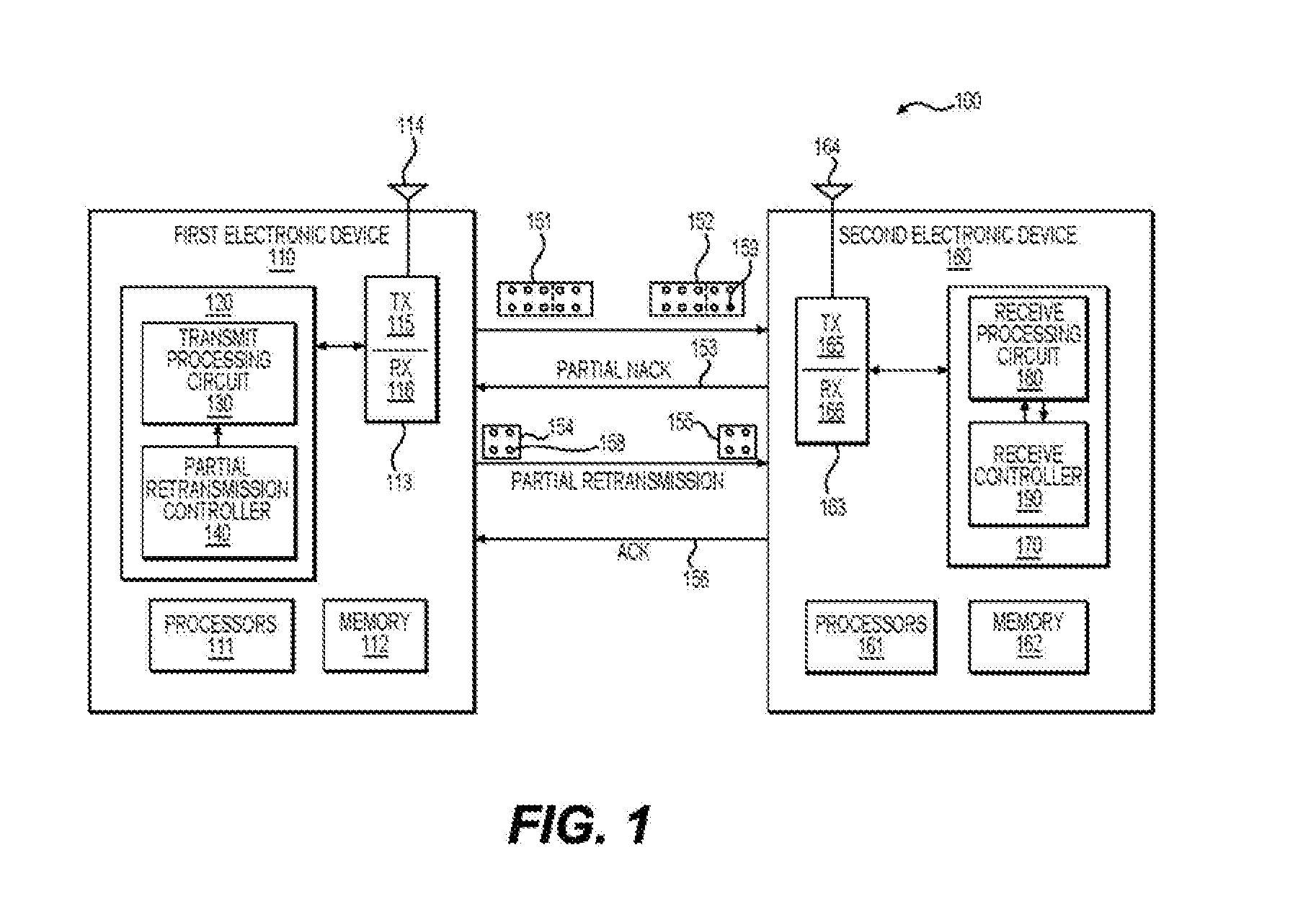
[0022] FIG. 1 shows a block diagram of an exemplary communication system 100 according to an embodiment of the disclosure. The communication system 100 includes a first electronic device 110 and a second electronic device 160 that communicate using wireless signals. The first electronic device 110 and the second electronic device 160 are configured to transmit wireless signals carrying data units and perform retransmission in response to receiving failures. Further, the first electronic device 110 and the second electronic device 160 are configured to transmit a portion of the initial transmission during the retransmission to improve communication efficiency.
[0023] The communication system 100 can be any suitable wireless communication system that uses suitable wireless communication technology, such as second generation (2G) mobile network technology, third generation (3G) mobile network technology, fourth generation (4G) mobile network technology, fifth generation (5G) mobile network technology, global system for mobile communication (GSM), long-term evolution (LTE), a New Radio (NR) access technology, a wireless local area network (WLAN), and the like.
[0024] In an example, one of the first electronic device 110 and the second electronic device 160 is an interface node in a telecommunication service provider, and the other electronic device is a terminal device. For example, the first electronic device 110 is the interface node, and the second electronic device 160 is the terminal device, or the first electronic device 110 is the terminal device, and the second electronic device 160 is the interface node.
[0025] In an example, the interface node, such as a base transceiver station, a Node B, an evolved Node B, and the like, includes hardware components and software components configured to enable wireless communications between the interface node and electronic devices that have subscribed services of the telecommunication service provider. The interface node is suitably coupled with other nodes, such as core nodes, other interface nodes, and the like of the telecommunication service provider.
[0026] In an example, the terminal device is user equipment used by an end-user for mobile telecommunication, such as a cell phone, a smart phone, a tablet computer, a laptop, a wearable device and the like. In another example, the terminal device is a stationary device, such as a desktop computer. In another example, the terminal device is a machine type communication device, such as a wireless sensor, an Internet of things (IoT) device and the like.
[0027] According to an aspect of the disclosure, partial retransmission is used by the first electronic device 110 and the second electronic device 160 to improve communication efficiency. In the FIG. 1 example, the first electronic device 110 transmits a data unit 151 in the form of a plurality of sub data units in an initial transmission. In an example, the data unit 151 is a transport block that is transmitted in the form of a plurality of code blocks. The second electronic device 160 receives wireless signals that carry a plurality of transmitted sub data units 152. The transmitted sub data units 152 can be corrupted due to for example, noise, signal distortion, interference, and the like. For example, a transmitted sub data unit 159 received by the second electronic device 160 is different from the corresponding sub data unit that is transmitted by the first electronic device 110 in the initial transmission. The second electronic device 160 detects the corrupted sub data unit, and transmits a partial negative acknowledgement (NACK).
[0028] In an example, the partial NACK is indicative of one or more corrupted sub data units. For example, the partial NACK uses a bit map to indicate the one or more corrupted sub data units. In another example, the partial NACK is indicative of a subset of sub data units that includes the one or more corrupted sub data units. In an example, the partial NACK uses one bit to indicate an error in a group of sub data units. For example, the partial NACK uses two bits to indicate whether a first half and/or a second half of the sub data units has/have errors. It is noted that the partial NACK can use other suitable number of bits for different granularity. For example, the partial NACK can use three bits for 1/3 granularity.
[0029] In the FIG. 1 example, the first electronic device 110 receives the partial NACK, and then transmits a portion of the data unit 151, as shown by sub data units 154, that include a sub data unit 158 corresponding to the corrupted sub data unit 159 in the initial transmission. The second electronic device 160 receives a plurality of retransmitted sub data units as shown by 155. When the plurality of retransmitted sub data units 155 are correctly received, the second electronic device 160 combines the plurality of retransmitted sub data units 155 with the sub data units 152 from previous reception to construct a received data unit. When the received data unit is constructed with success, the second electronic device 160 sends an acknowledgement (ACK) 156 to inform the first electronic device 110.
[0030] According to an aspect of the disclosure, when a data unit for transmission is relatively large, the retransmission transmits a portion of the data unit, and saves communication resources for other usage. In an embodiment, the first electronic device 110 can transmit other suitable sub data units (not shown), such as new sub data units from another data unit, and the like, with the sub data units 154 during the retransmission.
[0031] In the FIG. 1 example, the first electronic device 110 transmits the data unit, and the second electronic device 160 receives the data unit. It is noted that the second electronic device 160 can be configured to transmit a data unit and the first electronic device 110 can be configured to receive the data unit in the same or similar manner in the example.
[0032] In the FIG. 1 example, specifically, the first electronic device 110 includes a first transceiver 113 and a first baseband processing circuit 120 coupled together. The first electronic device 110 includes other suitable components, such as processors 111, memory 112, and the like. The second electronic device 160 includes a second transceiver 163 and a second baseband processing circuit 170 coupled together. The second electronic device 160 includes other suitable components, such as processors 161, memory 162, and the like.
[0033] Further, in the example, the first baseband processing circuit 120 includes a transmit processing circuit 130 and a partial retransmission controller 140 coupled together. The second baseband processing circuit 170 includes a receive processing circuit 180 and a receive controller 190 coupled together.
[0034] It is noted that the first baseband processing circuit 120 can include other suitable components, such as a receive processing circuit (not shown) similarly configured as the receive processing circuit 180, a receive controller (not shown) similarly configured as the subset receive controller 190. Similarly, the second baseband processing circuit 170 can include other suitable components, such as a transmit processing circuit (not shown) similarly configured as the transmit processing circuit 130, a partial retransmit controller (not shown) similarly configured as the partial retransmission controller 140.
[0035] The first transceiver 113 is configured to receive and transmit wireless signals. In an example, the first transceiver 113 includes a receiving circuit RX 116 and a transmitting circuit TX 115. The receiving circuit RX 116 is configured to generate electrical signals in response to captured electromagnetic waves by an antenna 114, and process the electrical signals to extract digital samples from the electrical signals. For example, the receiving circuit RX 116 can filter, amplify, down convert, and digitalize the electrical signals to generate the digital samples. The receiving circuit RX 116 can provide the digital samples to the first baseband processing circuit 120 for further processing.
[0036] In an example, the transmitting circuit TX 115 is configured to receive digital stream (e.g., output samples) from the first baseband processing circuit 120, process the digital stream to generate radio frequency (RF) signals, and cause the antenna 114 to emit electromagnetic waves in the air to carry the digital stream. In an example, the transmitting circuit TX 115 can convert the digital stream to analog signals, and amplify, filter and up-convert the analog signals to generate the RF signals.
[0037] The transmit processing circuit 130 is configured to receive a data unit and generate the digital stream corresponding to the data unit. In an example, the processors 111 execute software instructions to form upper layers of a protocol stack, and the processors 111 generate a transport block, which is a data unit for transport, following the protocol stack. In an example, the bottom of the upper layers of protocol stack is a data link layer, the data link layer outputs the transport block, and the processors 111 provide the transport block to the first baseband processing circuit 120. The first baseband processing circuit 120 forms a physical layer for the protocol stack in an example. The transmit processing circuit 130 receives the transport block and processes the transport block to generate the digital stream, and provide the digital stream to the transmitting circuit TX 115 for transmission.
[0038] In an example, the transmit processing circuit 130 partitions the transport block into a plurality of code blocks for example when the transport block is larger than a predetermined threshold. The transmit processing circuit 130 then processes the code blocks according to suitable coding and modulation scheme. For example, the code blocks can be encoded for example using suitable channel coding techniques, such as error detection coding technique, rate matching coding technique, low density parity check (LDPC) coding technique, polar coding technique and the like. The processed the code blocks are suitably modulated and multiplexed to generate the digital stream. For example, the code blocks can be modulated using suitable modulation technique, such as quadrature phase shift keying (QPSK), quadrature amplitude modulation (QAM), 16QAM, 64QAM, 256QAM, and can be multiplexed using suitable multiplexing technique, such as frequency-division multiplexing (FDM), time-division multiplexing (TDM), a combination of FDM and TDM, and the like.
[0039] Additionally, in the FIG. 1 example, the transmit processing circuit 130 is configured to generate the digital stream based on control signals from the partial retransmission controller 140. In an example, the transport block or the code blocks are suitably buffered after the initial transmission. When the first electronic device 110 receives the partial NACK that is indicative of partial receiving failure, the partial retransmission controller 140 determines control signals based on the partial receiving failure. In an example, the code blocks are suitably grouped into multiple code block groups (CBGs), and the partial NACK is indicative a receiving failure of a CBG of the transport block. The partial retransmission controller 140 can provide the control signals to the transmit processing circuit 130, such that the code blocks in the CBG are selectively processed to generate a digital stream for retransmission.
[0040] It is noted that, in an example, the size of the CBG is configurable under the control signals of the partial retransmission controller 140. In addition, in an example, the size of the CBG can be dynamically changed during operation for example under the control signals of the partial retransmission controller 140.
[0041] Similarly, the second transceiver 163 is configured to receive and transmit wireless signals. In an example, the second transceiver 163 includes a receiving circuit RX 166 and a transmitting circuit TX 165. The receiving circuit RX 166 is configured to generate electrical signals in response to captured electromagnetic waves by an antenna 164, and process the electrical signals to extract digital samples from the electrical signals. For example, the receiving circuit RX 166 can filter, amplify, down convert, and digitalize the electrical signals to generate the digital samples. The receiving circuit RX 166 can provide the digital samples to the second baseband processing circuit 170 for further processing.
[0042] In an example, the transmitting circuit TX 165 is configured to receive a digital stream (e.g., output samples) from the second baseband processing circuit 170, process the digital stream to generate radio frequency (RF) signals, and cause the antenna 164 to emit electromagnetic waves in the air to carry the digital stream. In an example, the transmitting circuit TX 165 can convert the digital stream to analog signals, and amplify, filter and up-convert the analog signals to generate the RF signals.
[0043] In the FIG. 1 example, the second baseband processing circuit 170 is configured to receive and process digital samples received from the receiving circuit RX 166 and provide digital streams to the transmitting circuit TX 165. In an embodiment, in the second baseband processing circuit 170, the receive processing circuit 180 is configured to receive the digital samples, process the digital samples to generate a decoded data unit and provide the decoded data unit to the processors 161 for further processing. In an example, the processors 161 execute software instructions to form upper layers of a protocol stack, and the processors 161 can process the decoded data unit following the protocol stack. In an example, the second baseband processing circuit 170 forms a physical layer for the protocol stack, the bottom of the upper layers formed by the processors 161 is a data link layer. The physical layer can output the data unit in the form of a transport block and provide the transport block to the data link layer for further processing.
[0044] In an embodiment, the receive processing circuit 180 receives first digital samples of the initial transmission, de-multiplexes and demodulates the first digital samples to generate first received code blocks, and decodes the first received code blocks. In an example, when the code blocks are received with success, the first received code blocks are decoded without error, then the second electronic device 160 sends the ACK to inform the first electronic device 110. However, when one or more code blocks are decoded with errors, the second baseband processing circuit 170 prepares the partial NACK to indicate partial receiving errors. In an example, the partial NACK is indicative of a receiving failure of a CBG that includes the one or more code blocks that are decoded with errors. In another example, the partial NACK is indicative of the one or more code blocks that are received with errors. The partial NACK is sent by the transmitting circuit TX 166 via the antenna 164 in an example.
[0045] In an example, the first electronic device 110 retransmits the CBG in response to the partial NACK. When the second electronic device 160 receives the wireless signals that carry the retransmission of the CBG, the receiving circuit RX 166 generates second digital samples of the retransmission. The receive processing circuit 180 receives the second digital samples of the retransmission, de-multiplexes and demodulates the second digital samples to generate second received code blocks, and decodes the second received code blocks. When the second received code blocks are decoded without errors, in an example, the receive controller 190 can cause the decoded code blocks from the initial transmission and the retransmission to be combined into a decoded transport block. The decoded transport block is provided to the processors 161 for further processing, and the second electronic device 160 sends the ACK to the first electronic device 110 in an example.
[0046] It is noted that the first baseband processing circuit 120 and the second baseband processing circuit 170 can be respectively implemented using various techniques. In an example, a baseband processing circuit is implemented as integrated circuits. In another example, a baseband processing circuit is implemented as one or more processors executing software instructions.
[0047] It is also noted that while single antenna per device is used in the FIG. 1 example, the communication 100 can be suitably modified to use multiple input, multiple output (MIMO) antenna technology.
[0048] FIG. 2 shows a block diagram of an exemplary baseband processing circuit 220 according to an embodiment of the disclosure. In an example, the baseband processing circuit 220 is used in the first electronic device 110 in the place of the first baseband processing circuit 120.
[0049] The baseband processing circuit 220 includes a transmit processing circuit 230 and a partial retransmission controller 240 coupled together as shown in FIG. 2. The transmit processing circuit 230 further includes a de-multiplexer (DEMUX) 231, a plurality of code block processing paths 235a-235n, a channel multiplexer (MUX) 237 and a modulator 238 coupled together. In the FIG. 2 example, each of the code block processing paths 235a-235n includes suitable circuit components, such as an encoder 232, a symbol mapper 233, and the like for processing a code block.
[0050] In the FIG. 2 example, the DEMUX 231 is configured to receive a transport block of a data packet. In an example, suitable error detection bits are added into the transport block for transport block level error detection. The DEMUX 231 is configured to partition the transport block into a plurality of code blocks. The plurality of code blocks are respectively processed by the plurality of code block processing paths 235a-235n. In an example, the encoder 232 can encode a code block according to suitable channel coding scheme and code rate. For example, the encoder 232 can encode the code block using an error detection code scheme, such as an LDPC coding technique, for code block level error detection. The symbol mapper 233 maps the code block to data symbols according to suitable modulation scheme. The channel MUX 237 can interleave and multiplex the data symbols from the plurality of code block processing paths 235a-235n according to the suitable multiplex scheme and the modulation scheme to provide a set of output symbols for subcarriers in each symbol period in an example. The modulator 238 then performs modulation and generates output samples.
[0051] The partial retransmission controller 240 can provide control signals to the transmit processing circuit 230 to select a subset of code blocks for a transport block, and generate the output samples corresponding to the selected code blocks. In an example, the partial retransmission controller 240 can generate the control signals in response to a partial NACK from a recipient of the transport block. In an example, the partial NACK is indicative of a receiving failure of a CBG. In an embodiment, the partial retransmission controller 240 provides the control signals respectively to the code block processing paths 235a-235n to selectively enable code block processing paths for the CBG, and disable the other code block processing paths during the partial retransmission of the transport block, thus output samples correspond to the CBG during the partial retransmission of the transport block. In another embodiment, the partial retransmission controller 240 provides the control signals to the channel MUX 237 to control the channel MUX 237 to generate the output samples corresponding to the CBG during the partial retransmission of the transport block.
[0052] It is noted that the baseband processing circuit 220 can be implemented using various techniques. In an example, the baseband processing circuit 220 is implemented as integrated circuits. In another example, the baseband processing circuit 220 is implemented as one or more processors executing software instructions.
[0053] FIG. 3 shows a block diagram of an exemplary baseband processing circuit 370 according to an embodiment of the disclosure. In an example, the baseband processing circuit 370 is used in the second electronic device 160 in the place of the second baseband processing circuit 170.
[0054] The baseband processing circuit 370 includes a receive processing circuit 380, an ACK/NACK generator 395, and a receive controller 390 coupled together as shown in FIG. 3. The receive processing circuit 380 further includes a demodulator 381, a channel de-multiplexer (DEMUX) 382, a plurality of code block processing paths 385a-385n, a multiplexer (MUX) 387 coupled together. Each of the code block processing paths 385a-385n includes suitable components, such as an statistical calculator 383, a decoder 384, and the like for processing a code block.
[0055] In an embodiment, the baseband processing circuit 370 receives first digital samples corresponding to an initial transmission of a transport block, and process the first digital samples to generate first decoded code blocks. For example, the demodulator 381 is configured to receive the first digital samples, perform demodulation on the first digital samples to generate data symbols of subcarriers during each of the symbol periods. The channel DEMUX 382 separates data symbols for the subcarriers during each symbol period, and determines data symbols respectively for code blocks, and provides the data symbols corresponding to the code blocks to the respective code block processing paths 385a-385n.
[0056] The code block processing paths 385a-385n respectively process data symbols for the code blocks. For example, the statistical calculators 383a-383n can respectively perform statistical computation, such as log-likelihood ratio computation on the received data symbols. The decoders 384a-384n then respectively decode the first code blocks based on the statistical computations in an example. The decoders 384a-384n can also check whether the decoding of the first code blocks are successful for example based on the error detection at the code block level.
[0057] In an embodiment, the MUX 387 can multiplex the first code blocks from the code block processing paths 385a-385n to form a decoded transport block when the first code blocks are decoded with success.
[0058] In the FIG. 3 example, the error detection results are provided to the ACK/NACK generator 395 to generate ACK or partial NACK. In an example, when one or more code blocks of the first decoded code blocks failed decoding, the ACK/NACK generator 395 generates the partial NACK indicative of a CBG that includes the one or more code blocks. In an embodiment, the partial NACK is transmitted, and the baseband processing circuit 370 receives second digital samples corresponding a retransmission of the CBG. The baseband processing circuit 370 can similarly process the second digital samples to generate second code blocks for the CBG.
[0059] In an embodiment, the receive controller 390 can suitably buffer the portion of the first code blocks that are decoded with success. When the second code blocks are decoded with success, the receive controller 390 can cause the second code blocks and the first code blocks to be combined to generate a decoded transport block. In an example, the receive controller 390 can provide the buffered first code blocks to the MUX 387, and the MUX 387 can multiplex the buffered first code blocks with the second code blocks to generate the decoded transport block. When the decoded transport block is decoded with success, the ACK/NACK generator 395 generates an ACK that is indicative of a receiving success of the transport block. The ACK is then transmitted.
[0060] It is noted that the baseband processing circuit 370 can be implemented using various techniques. In an example, the baseband processing circuit 370 is implemented as integrated circuits. In another example, the baseband processing circuit 370 is implemented as one or more processors executing software instructions.
[0061] FIG. 4 shows a flow chart outlining a process example 400 according to an embodiment of the disclosure. In an example, the process 400 is executed by a baseband processing circuit, such as the first baseband processing circuit 120 in the FIG. 1 example, the baseband processing circuit 220 in the FIG. 2 example, and the like with other suitable circuit, such as the first transceiver circuit 113. The process starts at 5401 and proceeds to 5410.
[0062] At 5410, a transport block for transmission is received. In the FIG. 1 example, the processors 111 execute software instructions to form upper layers of a protocol stack and the first baseband processing circuit 120 forms the physical layer of the protocol stack. The processors 111 generate a transport block, which is a data unit for transport. In an example, the data link layer in the protocol stack outputs the transport block to the first baseband processing circuit 120.
[0063] At 5420, the transport block is processed in the form of a plurality of code blocks. In the FIG. 2 example, the DEMUX 231 is configured to partition the transport block into a plurality of code blocks. The plurality of code blocks are respectively processed by the plurality of code block processing paths 235a-235n. The channel MUX 237 can interleave and multiplex the data symbols from the plurality code block processing paths 235a-235n to provide a set of output symbols for subcarriers in each symbol period in an example. The modulator 238 then performs modulation on the set of output symbols for subcarriers in each symbol period and generates first output samples.
[0064] At 5430, wireless signals are transmitted to carry the plurality of code blocks. In the FIG. 1 example, the transmitting circuit TX 115 receives the first output samples from the first baseband processing circuit 120, processes the first output samples to generate radio frequency (RF) signals, and causes the antenna 114 to emit electromagnetic waves corresponding to the RF signals in the air.
[0065] At 5440, a partial NACK is received. The partial NACK is indicative of a partial receiving failure of the code blocks. In an example, when one or more code blocks are received with decoding errors, the partial NACK is indicative of a receiving failure of a CBG that includes the one or more code blocks with decoding errors. In another example, the partial NACK is indicative of the one or more code blocks with decoding errors.
[0066] At 5450, wireless signals are transmitted to carry a CBG. In the FIG. 2 example, in an embodiment, the partial retransmission controller 240 provides the control signals respectively to the code block processing paths 235a-235n to selectively enable code block processing paths for the CBG, and to disable the other code block processing paths during the partial retransmission of the transport block. In another embodiment, the partial retransmission controller 240 provides the control signals to the channel MUX 237 to control the channel MUX 237 to generate second output samples corresponding to the CBG during the partial retransmission. Then a transmitting circuit, such as the transmitting circuit TX 115, receives the second output samples, processes the second output samples to generate radio frequency (RF) signals, and causes the antenna 114, to emit electromagnetic waves corresponding to the RF signals in the air.
[0067] At 5460, an ACK is received. In the FIG. 1 example, when the second electronic device 160 receives the wireless signals that carry the retransmission of the CBG, the second electronic device 160 combines decoded code blocks from the initial transmission and the partial retransmission to generate a decoded transport block. When the decoded transport block is decoded with success, the second electronic device 160 sends the ACK, and the first electronic device 110 receives the ACK indicative of the decoding success of the transport block. The process proceeds to 5499 and terminates.
[0068] FIG. 5 shows a flow chart outlining a process example 500 according to an embodiment of the disclosure. In an example, the process 500 is executed by a baseband processing circuit, such as the second baseband processing circuit 170, the baseband processing circuit 370, and the like with other suitable circuit, such as the second transceiver circuit 163. The process starts at 5501 and proceeds to 5510.
[0069] At 5510, wireless signals carrying a transport block are received. The wireless signals carry the transport block in the form of a plurality of code blocks. In the FIG. 1 example, during an initial transmission of a transport block, the transmitting circuit TX 115 receives the first output samples from the first baseband processing circuit 120, processes the first output samples to generate radio frequency (RF) signals, and causes the antenna 114 to emit electromagnetic waves corresponding to the RF signals in the air. The receiving circuit RX 166 is configured to generate electrical signals in response to captured electromagnetic waves by the antenna 164, and process the electrical signals to extract first digital samples from the electrical signals.
[0070] At 5520, code blocks are respectively processed and decoded. In the FIG. 3 example, the demodulator 381 is configured to receive the first digital samples, perform demodulation on the first digital samples to generate data symbols of subcarriers during each of the symbol periods. The channel DEMUX 382 separates data symbols for the subcarriers during each symbol period, and determines data symbols respectively for code blocks, and provides the data symbols corresponding to the code blocks to the respective code block processing paths 385a-385n. The code block processing paths 385a-385n respectively process data symbols for the code blocks. For example, the statistical calculators 383a-383n can respectively perform statistical computation, such as log-likelihood ratio computation on the received data symbols. The decoders 384a-384n then respectively decode the first code blocks based on the statistical computations in an example.
[0071] At 5530, one or more code blocks are decoded with errors. In the FIG. 3 example, the decoders 384a-384n can also check whether the first code blocks are decoded with success for example based on the error detection at the code block level. In the example, one or more code blocks are decoded with errors.
[0072] At 5540, a partial NACK is transmitted. The partial NACK is indicative of a partial receiving failure. In the FIG. 3 example, when one or more code blocks of the first decoded code blocks failed decoding, the ACK/NACK generator 395 generates the partial NACK indicative of a receiving failure of a CBG that includes the one or more code blocks.
[0073] At 5550, wireless signals carrying a CBG in a retransmission are received. In the FIG. 2 example, in an embodiment, the partial retransmission controller 240 provides the control signals to the channel MUX 237 to control the channel MUX 237 to generate second output samples corresponding to the CBG during the partial retransmission. Then a transmitting circuit, such as the transmitting circuit TX 115, receives the second output samples, processes the second output samples to generate radio frequency (RF) signals, and causes the antenna 114, to emit electromagnetic waves corresponding to the RF signals in the air. The receiving circuit RX 166 is configured to generate electrical signals in response to captured electromagnetic waves by the antenna 164, and process the electrical signals to extract second digital samples from the electrical signals.
[0074] At 5560, code blocks of CBG are respectively processed and decoded. In the FIG. 3 example, the baseband processing circuit 370 receives the second digital samples corresponding the retransmission of the CBG. The baseband processing circuit 370 can process the second digital samples to generate second code blocks corresponding to the CBG.
[0075] At 5570, the decoded code blocks from the partial retransmission and previous transmission are combined to generate the decoded transport block. In the FIG. 3 example, the receive controller 390 can suitably buffer the portion of the first code blocks that are decoded with success. When the second code blocks are decoded with success, the receive controller 390 can cause the second code blocks and the first code blocks to be combined to generate a decoded transport block.
[0076] At 5580, an ACK is transmitted. In the FIG. 3 example, when the decoded transport block is decoded with success, the ACK/NACK generator 395 generates an ACK that is indicative of a receiving success of the transport block. The ACK is then transmitted. Then the process proceeds to 5599 and terminates.
[0077] When implemented in hardware, the hardware may comprise one or more of discrete components, an integrated circuit, an application-specific integrated circuit (ASIC), etc.
[0078] While aspects of the present disclosure have been described in conjunction with the specific embodiments thereof that are proposed as examples, alternatives, modifications, and variations to the examples may be made. Accordingly, embodiments as set forth herein are intended to be illustrative and not limiting. There are changes that may be made without departing from the scope of the claims set forth below.
* * * * *
D00000
D00001
D00002
D00003
D00004
XML
uspto.report is an independent third-party trademark research tool that is not affiliated, endorsed, or sponsored by the United States Patent and Trademark Office (USPTO) or any other governmental organization. The information provided by uspto.report is based on publicly available data at the time of writing and is intended for informational purposes only.
While we strive to provide accurate and up-to-date information, we do not guarantee the accuracy, completeness, reliability, or suitability of the information displayed on this site. The use of this site is at your own risk. Any reliance you place on such information is therefore strictly at your own risk.
All official trademark data, including owner information, should be verified by visiting the official USPTO website at www.uspto.gov. This site is not intended to replace professional legal advice and should not be used as a substitute for consulting with a legal professional who is knowledgeable about trademark law.